solving_mipi_d-phy_receiver test challenges
- 格式:pdf
- 大小:540.13 KB
- 文档页数:11
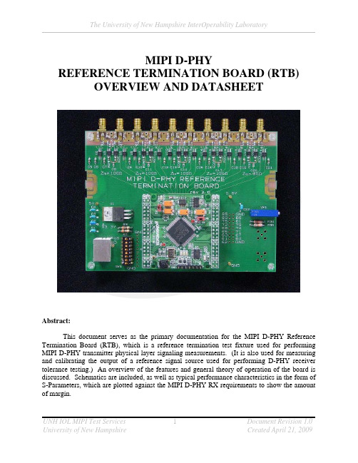
MIPI D-PHYREFERENCE TERMINATION BOARD (RTB) OVERVIEW AND DATASHEETAbstract:This document serves as the primary documentation for the MIPI D-PHY Reference Termination Board (RTB), which is a reference termination test fixture used for performing MIPI D-PHY transmitter physical layer signaling measurements. (It is also used for measuring and calibrating the output of a reference signal source used for performing D-PHY receiver tolerance testing.) An overview of the features and general theory of operation of the board is discussed. Schematics are included, as well as typical performance characteristics in the form of S-Parameters, which are plotted against the MIPI D-PHY RX requirements to show the amount of margin.Introduction:The MIPI D-PHY Reference Termination Board (RTB) is a reference test fixture that is designed to emulate ‘ideal’ best-case and worst-case reference D-PHY receiver termination characteristics. It is implemented in the form of an actively-controlled HS resistive load, which is enabled and disabled with the appropriate timings via FPGA control, according to the MIPI D-PHY LP signaling protocol. The fixture enables the measurement of most HS voltage and timing parameters using a single measurement setup, and the board is designed with very precisely controlled impedance and termination characteristics, in order to present a consistent, repeatable, termination environment to D-PHY transmitters for the purpose of performing MIPI-D-PHY transmitter physical layer conformance testing (and also for calibrating the output of lab signal sources when performing D-PHY receiver tolerance testing.) The board is meant to be used in conjunction with a real-time DSO and the necessary probing, accessories, and analysis software required for performing D-PHY measurements. (For more information about general D-PHY test equipment requirements, as well as test definitions, setups, and procedures, please refer to the MIPI D-PHY Physical Layer Conformance Test Suite document, which is freely available to MIPI Members via the MIPI Testing Program Page.)Background:Unlike many other high-speed serial technologies that utilize a static, 100-ohm differential reference termination environment, MIPI D-PHY is somewhat unique in that one of the key power-saving aspects of D-PHY is it’s the fact that the link utilizes a dynamic, switchable resistive termination at the receiver, which is enabled during the High-Speed (HS) mode of operation, and disabled to present an open termination environment during Low-Power (LP) mode. The HS and LP modes utilize different signaling schemes, with different voltage levels. The LP mode of operation is designed such that data can still be communicated between the two ends of the link, but at a much lower speed (20Msymbols/sec max) than in HS mode, which is designed for operation between 80 and approximately 800 Mbps. This dual-mode functionality requires a different receiver architecture than that typically found in other high-speed serial technologies. A simplified diagram of an example receiver implementation is shown in Figure 1 below (which has been reproduced from the D-PHY specification.)Figure 1: Example D-PHY Receiver Termination DiagramIn LP mode, all wires are operated single-ended, and are unterminated at the receiver. In this mode, minimal current flows between the two ends of the link (due to the lack of an RX termination), which reduces power consumption. In HS mode, the link utilizes differential signaling, but with a lower amplitude level than most other high-speed serial technologies, and also with a common-mode DC offset (whereas most other high-speed serial technologies are AC-coupled, and use DC-balanced signaling levels in conjunction with 8B/10B encoding).D-PHY devices switch between HS and LP modes via communication of a special LP state sequence, which signals an intent to transition to HS mode. When a receiver detects this mode it will enable its High-Speed (HS) line termination, which prepares the line for HS operation. The transmitter is then able to transmit data at the HS line rate for a period of time, after which a different control sequence is sent, which initiates a return to the LP mode of operation (whereby the receiver disconnects its HS termination at the appropriate time). This act of switching in and out of HS mode is typically called HS ‘burst mode’ operation.In most other high-speed serial technologies that utilize a static, 100-ohm differential termination environment with DC-balanced signaling, it is common to use the test equipment input ports as the reference termination load for measurements, as the front end inputs of most pieces of test equipment are 50-ohm terminated, which effectively looks like a 50-ohm resistance to ground. By splitting the differential signal into two halves, and terminating each half into 50 ohms, a 100-ohm differential termination is achieved. This is typically the approach used for technologies like SATA, SAS, PCI Express, XAUI, 10GBASE-CX4, etc. For all of these standards, the test equipment basically provides a common, reference termination environment which is relatively consistent between different pieces of test equipment, as the termination specifications for the inputs of lab test equipment are typically very tightly controlled.D-PHY however, presents a somewhat unique challenge, as there are two main factors that prevent using the test equipment (oscilloscope in this case) as the reference termination. The first is simply the presence of the switching open/100-ohm receiver termination, which no standard test instrument is capable of duplicating. The second factor is the fact that the HS mode of D-PHY expects the receiver to be AC coupled to ground, so that a DC common-mode offset may be applied to the HS signal. If the HS differential signal is split and sent into two 50-ohm input ports of a DSO, the transmitter’s common mode signal component does not see an AC-coupled path to ground, but rather a 25-ohm DC path to ground (created by the two 50-ohm input resistances in parallel.) This is not the termination for which the transmitter was designed, and thus prevents this type of measurement setup from being used.Another measurement approach that is used to measure high-speed serial signals is to terminate the desired signal with an external termination load, and then probe the signal at that termination point using a high-impedance active differential probe. These high-performance probes use active circuitry to observe the signal under test without disturbing the signal itself, or causing excessive additional loading to the transmitter.In this environment, the quality of the signal observed depends heavily on the electrical characteristics and quality of the external termination element used to terminate the line, as wellas the quality of the means used to physically attach the termination element (typically a resistor) to the line. Hand-soldering of discrete components to a transmitter output port is typically not precise enough to produce consistent, repeatable results. Furthermore, this still does not address the switching nature of the D-PHY termination environment. Because of these issues, and the need to demonstrate accurate, repeatable physical layer measurements for D-PHY, there arose a need for a specialized, laboratory-grade termination solution for D-PHY test purposes.The Solution:To meet the need for a single common reference termination solution for D-PHY, the D-PHY Reference Termination Board (RTB) was developed, and is intended to serve as a common reference test fixture to facilitate consistent and repeatable conformance measurements of MIPI D-PHY signaling, for both conformance and characterization purposes.A detailed image of the RTB is shown in the figure below, with icons highlighting several of the key features, which are described in further detail below.Figure 2: Detailed View of RTB (Top Side)Features:Several key features of the RTB highlighted in Figure 2 above are:1) SMA Inputs with Recommended Spacing and Lane Ordering:The RTB uses standard SMA RF connectors. This is the means by which the RTB is connected to the Device Under Test (DUT). The RTB supports up to five D-PHY Lanes (1 Clock + 4 Data), and uses a common SMA spacing and Lane pinout recommended by UNH IOL for D-PHY test board designs, commonly known as the Test Vehicle Board (TVB) recommendations. The purpose of specifying a common spacing and Lane ordering is to allow devices that implement the TVB spacing and pinout to be mated directly to one another using only SMA male-to-male couplers. This eliminates the need for additional SMA cables for connecting devices together, and provides the best possible quality signal path between devices.The spacing of the SMA connectors is 500-mil, center-to-center, for all connectors. The Lane ordering is (reading left to right in Figure 2 above): ClkN, ClkP, Data0N, Data0P, Data1N, Data1P, Data2N, Data2P, Data3N, Data3P.Note that the recommended Lane ordering is optimized for testing peripheral devices (e.g., Camera Sensors or Displays), however the RTB can also be used for testing Host DUTs, by simply flipping the RTB upside-down, which reverses the pinout. The recommended lane ordering is shown graphically below, for both Hosts and Peripherals.Figure 3: Recommended Lane Ordering for DUT Evaluation Boards2) Controlled-Impedance SMA Launches:In order to optimize the connection path between devices, care must be taken to minimize impedance discontinuities that can occur at and around the SMA connectors of test boards. The area where the signal transitions from the pin of the SMA connector into the PCB trace is commonly called the launch. Poor quality SMA connectors, and/or poor PCB launch design can result in impedance discontinuities that will cause reflections to occur, resulting in reduced signal integrity, and other signaling artifacts, which are not acceptable when trying to make accurate measurements. The RTB uses a specially designed launch, customized for the specific SMA connector used, which minimizes the impedance discontinuity introduced by the SMA connectors. By using controlled launches on both the RTB and the DUT’s evaluation PCB, signals can pass through the SMA interface between boards with minimal degradation.3) Active-Switching Termination Structure:The small components seen just after the launch structure make up the HS termination structure. The structure for each Lane consists of two ADG8611 Ultrafast 4ns Single-Supply Comparators (which buffer the signal and are used to determine the high/low state of the line in LP mode), and two ADG902 Wideband 1GHz CMOS Switches, which perform the actual switching of the HS termination resistor (commonly referred to as ZID in the D-PHY specification), which is also implemented as part of the termination structure (see the small SMD resistors located between the switches/comparators, and the SMA launches).The termination structures are specifically designed to be located as near to the SMA launches as possible, in order to minimize the excess trace length, and hence the capacitive loading seen by the DUT transmitter.4) FPGA For Termination Control and Timing:The termination switch structure alone is not sufficient to accomplish the switching operation. The purpose of the ADG8611 comparators is actually to sense the line and determine the LP line state during regular DUT operation. The output of the comparators is sent to the inputs of the FPGA, which is programmed to understand the LP signaling protocol, and looks for the proper ‘HS-entry’ sequence of LP states (LP-11/LP-01/LP-00), at which point it triggers the ADG902 switches to close and enable the HS termination resistor (ZID), in preparation for HS mode.Once HS mode is enabled, the FPGA is programmed to look for the end of the HS burst (signaled by a return to the LP-11 state), at which point it disconnects the HS termination by deactivating the ADG902 switches.5) Manual Override Dipswitches:Because there are cases where it may be necessary to force the HS termination on or off (for example, in the case of a CSI-2 transmitter that supports Continuous Clocking, in which case LP signaling is not used on the Clock Lane, as the HS clock is transmitted continuously and does not return to LP mode between bursts), the dipswitches (SW1) on the RTB may be used to override the FPGA control, and manually force the HS terminations on or off.The dipswitches allow independent control of the Clock Lane and the group of four Data Lanes, and work as follows:DIPSW8: ON : CLK Lane Termination always ONDIPSW7: ON: CLK Lane Termination always OFFDIPSW6: ON: DATA0/1/2/3 Lane Termination always ONDIPSW5: ON: DATA0/1/2/3 Lane Termination always OFFFor example, if you want to force the Clock Lane termination ON (for a continuous-clocking DUT), then you would turn DIPSW8 to ON, and rest of switches to OFF6) Power Supply (USB):The RTB receives power via a standard USB connection to any USB host port. (Note the USB connection is only used to supply power, and does not perform data transfer of any kind.)The 5V supply voltage from the USB port is stepped down to 3.3V via the LM1117T regulator, which supplies power to all of the other active components on the board.7) Comparator Reference Level Adjustment:The two comparators per Lane are used to buffer the incoming signals, and effectively make a digital copy of each single-ended LP signal, which is sent back to the FPGA. The comparators compare the observed line level against a reference voltage level, and output a logic 1 or 0 if the line level is higher or lower than the reference voltage, respectively.The comparator reference level is set to 0.6V by default, as this is approximately one-half of the typical nominal LP signaling level of 1.2V. The FPGA is programmed to enable the HS termination at a specific time after the last falling LP edge of the HS entry sequence (LP-11/LP-10/LP-00). In rare cases where the FPGA does not appear to be enabling the HS termination at the proper time, it may be possible to adjust this value by modifying the comparator’s reference voltage level, which may have some effect if the LP edges of the DUT have an especially slow fall time. (Again, this should never really be necessary under typical conditions.) Thecomparator reference level can be measured using a multimeter at pin marked ‘0.6V’, located near the blue potentiometer. The level can then be adjusted via the blue potentiometer (VR1), using a small screwdriver.8) Worst-Case ZID Values (Lanes Data2 and Data3):The final feature of the RTB worth noting is the fact that the RTB does not use the same ZID resistance value for all Lanes.The D-PHY specification requires several of the HS-TX signaling requirements to be met, ‘for all possible values of ZID’. This includes the HS rise/fall times, as well as VCMTX, VOD, and VOHHS. For the purpose of measuring these values under the ‘worst-case’ ZID values (i.e., the maximum and minimum values defined in the spec), the Data2 and Data3 Lanes of the RTB are designed with ZID values of 125 and 80 ohms, respectively (while the Clock, Data0, and Data1 Lanes all designed with ZID = 100 ohms by default). These Lanes can be used to terminate individual DUT Lanes for the purpose of these amplitude-specific measurements. (Note that in these cases the Clock Lane of the RTB will not mechanically align to the Clock Lane of the DUT, however depending on the measurement software being used, a Clock Lane signal may not be required to perform the amplitude-specific measurements that require being tested with the worst-case ZID values.Note also that the standard RTB configuration is optimized for DUT’s having up to 2 Data Lanes. For DUTs with 3 or 4 Data Lanes, it may be necessary to use short SMA cables to remap the DUT’s Data Lanes 3 and 4 to the RTB’s Data Lanes 0 and 1 for some HS measurements, where both Clock and Data Lane signals need to be measured simultaneously into ZID values of 100 ohms (e.g., clock-to-data skew). In these cases the SMA cables should be as short as possible, and should also be matched in terms of electrical length, to minimize additional skew.One additional note regarding the ZID resistor values: All Lanes of the RTB are functionally identical, and independently controlled by the FPGA. The only real difference is the ZID values for the Data2 and Data3 Lanes. Technically it would be possible to modify/remap the ZID values for any lane to any value or combination/order of values, by simply changing the two ZID resistors per lane (which are each approximately ZID/2, but are actually 1-2 ohms lower than this to account for the added resistance of the switches, which are effectively in series with the ZID resistors). Again, this should not need to be done under normal circumstances, but it is mentioned here for informative purposes only.Also, the common-mode termination capacitance (Ccm) is controlled by a single capacitor per Lane, and is designed with a value of 47pF for all Lanes, as this produces the optimal common-mode return loss characteristics (see S-Parameter data, in the last section of this document). This value can also technically be modified via a component change on the RTB, but again this should not be required under normal circumstances.Schematics:The schematics for the RTB are shown below. (Note that only the full circuit for the Clock Lane is shown, as the other four Lanes are identical, except for the values of the ZID resistors.)(Also note that a copy of the termination circuit schematic is also printed on the bottom silkscreen of the actual RTB PCB, for convenience.)Figure 4: RTB SchematicsImpedance and S-Parameter Data:The following pages contain impedance profile data and S-Parameter return loss data for the different Lanes of the RTB. Where applicable, the values are plotted against the D-PHY HS-RX S-Parameter requirements (i.e., the data is presented as if the RTB were tested as an actual D-PHY receiver device.)Data is presented for three Lanes: Clock, Data2, and Data3. The characteristics for Data Lanes 0 and 1are not shown because they are identical to the Clock Lane (i.e., ZID = 100 ohms for the Clock, Data0, and Data1 Lanes.)Note: The raw S-Parameter data source files used to generate these plots are available (for simulation purposes, etc), and can be obtained by contacting Andy Baldman at aab@.Clock Lane: Differential Impedance Profile and Return Loss (ZID = 100 ohms)Clock Lane: Common-Mode Impedance Profile and Return LossClock Lane: Differential Impedance ImbalanceData Lane 2: Differential Impedance Profile and Return Loss (ZID = 125 ohms)Data Lane 2: Common-Mode Impedance Profile and Return LossData Lane 2: Differential Impedance ImbalanceData Lane 3: Differential Impedance Profile and Return Loss (ZID = 80 ohms)Data Lane 3: Common-Mode Impedance Profile and Return LossData Lane 3: Differential Impedance Imbalance。

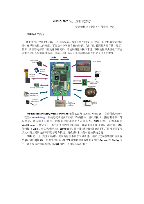
MIPI D-PHY简介及测试方法安捷伦科技(中国)有限公司李凯一、MIPI D-PHY简介对于现代的智能手机来说,其内部要塞入太多各种不同接口的设备,给手机的设计和元器件选择带来很大的难度。
下图是一个智能手机的例子,我们可以看到其内部存储、显示、摄像、声音等内部接口都是各不相同的。
即使以摄像头接口来说,不同的摄像头模组厂商也可能会使用不同的接口形式,这给手机厂商设计手机和选择器件带来了很大的难度。
MIPI (Mobile Industry Processor Interface)是2003年由ARM, Nokia, ST ,TI等公司成立的一个联盟(),目的是把手机内部的接口如摄像头、显示屏接口、射频/基带接口等标准化,从而减少手机设计的复杂程度和增加设计灵活性。
MIPI联盟下面有不同的WorkGroup,分别定义了一系列的手机内部接口标准,比如摄像头接口CSI、显示接口DSI、射频接口DigRF、麦克风/喇叭接口SLIMbus等。
统一接口标准的好处是手机厂商根据需要可以从市面上灵活选择不同的芯片和模组,更改设计和功能时更加快捷方便。
MIPI是一个比较新的标准,其规范也在不断修改和改进,目前比较成熟的接口应用有DSI(显示接口)和CSI(摄像头接口)。
CSI/DSI分别是指其承载的是针对Camera或Display应用,都有复杂的协议结构。
以DSI为例,其协议层结构如下:CSI/DSI的物理层(Phy Layer)由专门的WorkGroup负责制定,其目前采用的标准是D-PHY。
D-PHY采用1对源同步的差分时钟和1~4对差分数据线来进行数据传输。
数据传输采用DDR 方式,即在时钟的上下边沿都有数据传输。
D-PHY的物理层支持HS(High Speed)和LP(Low Power)两种工作模式。
HS模式下采用低压差分信号,功耗较大,但是可以传输很高的数据速率(数据速率为80M~1Gbps);LP模式下采用单端信号,数据速率很低(<10Mbps),但是相应的功耗也很低。

基于MIPI D-PHY规范的低速接收电路设计
张自豪;赵建中;周玉梅
【期刊名称】《电子设计工程》
【年(卷),期】2022(30)5
【摘要】文中基于MIPI D-PHY 1.1规范,提出了一种低速接收电路。
该低速接收电路通过线路电平产生内部异步低速时钟,进行引导码的检测;在ESC;MD和LPDT 状态下,通过Spaced-One-Hot解码电路产生进入命令码和低速有效数据。
搭建了D-PHY模拟电路模型,在TestBench平台上仿真验证了低速模式下LPDT、Trigger和ULPS模式之间的进入和退出测试用例。
分析DC逻辑综合时序报告,该低速模式接收电路满足D-PHY 1.1规范的数据速率要求。
【总页数】5页(P37-41)
【作者】张自豪;赵建中;周玉梅
【作者单位】中国科学院微电子研究所;中国科学院大学
【正文语种】中文
【中图分类】TN492
【相关文献】
1.MIPI接口高速接收电路设计
2.基于MIPI标准下的D-PHY的设计与验证
3.基于40nm CMOS工艺的25Gb/s光接收机模拟前端电路设计
4.基于水声换能器的驱动和接收电路设计
5.基于MIPI规范的从端D-PHY数字电路设计
因版权原因,仅展示原文概要,查看原文内容请购买。

MIPID-PHY简述1 概述mipi接⼝在视频领域⼴泛使⽤sensor和soc的接⼝是mipi csi-2soc和mipi屏的接⼝是mipi dsiD-PHY是⼴泛使⽤的物理层协议,除此之外,还要C-PHY和M-PHY。
我们只⽤到D-PHY,本⽂对D-PHY的简要说明。
2 接⼝简述2.1 lane如下图:两个通过MIPI通信的硬件,最底层由若⼲lane组成D-PHY⽀持最少1个clock+1个data lane,最多1个clock+4个data lane公司的视频芯⽚,2和4 lane指data lane,clock是必须的,没有包含在内clock lane总是单向的,data lane可双向,但实际应⽤中,只有DSI lane0实现为低速双向2.2 lane内部如下图:HS是high speedLP是low powerLP和HS都可以配置为双向CSI-2实际配置, HS单向, LP单向DSI实际配置,DATA0 有LP双向,HS单向,其他DATA LANE HS单向,LP单向针对这个全集的裁剪,有个表格,CIL-**表⽰裁剪内容,知道就好了2.3 Dp、Dn电特性HS 差分,LP单端HS 80~1500 Mbps,带deskew capability是最⼤到2500MbpsLP 最⼤10Mbps3 各种Lane State如下图:HS模式⽤于⾼速传输,进⼊和退出HS模式时,都需要在LP的control模式下做若⼲LP**操作⼀般在HS和LP的control模式之前切换Escape模式的作⽤是实现低速模式的通信,例如DSI的低速命令收发就是Escape的LPDT模式即使没有Escape模式,⼀般LP单向也是需要的,因为进出HS模式需要LP的control模式进⾏操只有从LP control模式才能进⼊Escape模式LP模式下,RX端不需要clk,但TX端需要⽤到,所以escape clk也是要配置的ULPS模式我们暂时没有⽤到下图是各个状态转换的状态机:参考Specification for D-PHY V1.2。
EMI4183MUCommon Mode Filter with ESD ProtectionFunctional DescriptionThe EMI4183MU is an integrated common mode filter providing both ESD protection and EMI filtering for high speed digital serial interfaces such as MIPI D-PHY .The EMI4183MU provides protection for three differential data line pairs in a small RoHS-compliant UDFN16 package.Features•Highly Integrated Common Mode Filter (CMF) with ESD Protection provides protection and EMI reduction for systems using High Speed Serial Data Lines with cost and space savings over discrete solutions •Large Differential Mode Bandwidth with Cutoff Frequency > 2 GHz •High Common Mode Stop Band Attenuation: >25 dB at 700 MHz,>30 dB at 800 MHz•Provides ESD Protection to IEC61000-4-2 Level 4, ±15 kV Contact Discharge•Low Channel Input Capacitance Provides Superior Impedance Matching Performance•Low Profile Package with Small Footprint in UDFN16 2 x 4 mm Pb −Free Package•These Devices are Pb −Free, Halogen Free/BFR Free and are RoHS CompliantApplications•MIPI D-PHY (CSI-2, DSI, etc) in Mobile Phones and Digital StillCamerasFigure 1. EMI4183MU Electrical SchematicExternal MARKING DIAGRAMSU3= Specific Device Code M = Date Code G = Pb −Free Package(*Note: Microdot may be in either location)PIN CONNECTIONSDevice Package Shipping †ORDERING INFORMATION†For information on tape and reel specifications,including part orientation and tape sizes, please refer to our T ape and Reel Packaging Specifications Brochure, BRD8011/D.EMI4183MUTAGUDFN16(Pb −Free)3000/T ape & ReelUDFN16CASE 517CKIn_1+In_1−Out_1+Out_1−In_2+In_2−Out_2+Out_2−GND GND In_3+In_3−GNDGND Out_3+Out_3−(Top View)U3M G GPIN FUNCTION DESCRIPTIONPin Name Pin No.Type DescriptionIn_1+1I/O CMF Channel 1+ to Connector (External)In_1−2I/O CMF Channel 1− to Connector (External)Out_1+16I/O CMF Channel 1+ to ASIC (Internal)Out_1−15I/O CMF Channel 1− to ASIC (Internal)In_2+4I/O CMF Channel 2+ to Connector (External)In_2−5I/O CMF Channel 2− to Connector (External)Out_2+13I/O CMF Channel 2+ to ASIC (Internal)Out_2−12I/O CMF Channel 2− to ASIC (Internal)In_3+7I/O CMF Channel 3+ to Connector (External)In_3−8I/O CMF Channel 3− to Connector (External)Out_3+10I/O CMF Channel 3+ to ASIC (Internal)Out_3−9I/O CMF Channel 3− to ASIC (Internal)GND3, 14GND GroundGND6, 11GND GroundABSOLUTE MAXIMUM RATINGS (T A= 25°C unless otherwise noted)Parameter Symbol Value Unit Operating Temperature Range T OP−40 to +85°CStorage Temperature Range T STG−65 to +150°CT L260°CMaximum Lead Temperature for Soldering Purposes(1/8” from Case for 10 seconds)DC Current per Line I LINE100mA Stresses exceeding Maximum Ratings may damage the device. Maximum Ratings are stress ratings only. Functional operation above the Recommended Operating Conditions is not implied. Extended exposure to stresses above the Recommended Operating Conditions may affect device reliability.ELECTRICAL CHARACTERISTICS (T A= 25°C unless otherwise noted)Symbol Parameter Test Conditions Min Typ Max UnitI LEAK Channel Leakage Current T A = 25°C, V IN = 5 V, GND = 0 V 1.0m AV F Channel Negative Voltage T A = 25°C, I F= 10 mA0.1 1.5VC IN Channel Input Capacitance to Ground(Pins 1,2,4,5,7,8 to Pins 3,6,11,14) T A = 25°C, At 1 MHz, GND = 0 V,V IN = 1.65 V0.8 1.3pFR CH Channel Resistance(Pins 1−16, 2−15, 4−13, 5−12, 7−10 & 8−9)8.0W f3dB Differential Mode Cut−off Frequency 50 W Source and Load Termination 2.0GHz F atten Common Mode Stop Band Attenuation @ 800 MHz30dBV ESD In−system ESD Withstand Voltagea) Contact discharge per IEC 61000−4−2standard, Level 4 (External Pins)b) Contact discharge per IEC 61000−4−2standard, Level 1 (Internal Pins) (Notes 1 and 2)±15±2kVV CL TLP Clamping Voltage(See Figure 12) Forward I PP= 8 AForward I PP= 16 AForward I PP= −8 AForward I PP= −16 A1218−6−12VVVVR DYN Dynamic ResistancePositive TransientsNegative Transients T A = 25°C, I PP= 1 A, t P = 8/20 m sAny I/O pin to Ground;(Notes 1 and 3)1.360.6V RWM Reverse Working Voltage (Note 3) 5.0V V BR Breakdown Voltage I T = 1 mA; (Note 4) 5.69.0V 1.Standard IEC61000−4−2 with C Discharge = 150 pF, R Discharge = 330, GND grounded.2.These measurements performed with no external capacitor.S devices are normally selected according to the working peak reverse voltage (V RWM), which should be equal to or greater than the DCor continuous peak operating voltage level.4.V BR is measured at pulse test current I T.TYPICAL CHARACTERISTICSFigure 2. Differential Mode Attenuation vs.Frequency (Zdiff = 100 W )Figure 3. Common Mode Attenuation vs.Frequency (Zcomm = 50 W )Figure 4. Differential Return Loss vs. Frequency(Zdiff = 100 W )Figure 5. Differential Inter −Lane Cross −CouplingFigure 6. Common Mode Inter −Lane Cross −CouplingFigure 7. MIPI D −PHY LP Mode Test SetupFigure 8. EMI4183MU MIPI D −PHY LP Mode Measured ResultsFigure 9. EMI4183MU Eye Diagram Test SetupEMI4183MU********************************************(EVBthroughonleft,EVBwithEMI4183MUonright)Transmission Line Pulse (TLP) MeasurementsTransmission Line Pulse (TLP) provides current versus voltage (I-V) curves in which each data point is obtained from a 100 ns long rectangular pulse from a charged transmission line. A simplified schematic of a typical TLP system is shown in Figure 11. TLP I-V curves of ESD protection devices accurately demonstrate the product’s ESD capability because the 10 s of amps current levels and under 100 ns time scale match those of an ESD event. This is illustrated in Figure 12 where an 8 kV IEC61000-4-2 current waveform is compared with TLP current pulses at 8 and 16 A. A TLP curve shows the voltage at which the device turns on as well as how well the device clamps voltage over a range of current levels. Typical TLP I-V curves for the EMI4183MU are shown in Figure 13.Figure 11. Simplified Schematic of a Typical TLP SystemFigure 12. Comparison Between 8 kV IEC61000−4−2 and 8 A and 16 A TLP WaveformsFigure 13. Positive and Negative TLP WaveformsESD Voltage ClampingFor sensitive circuit elements it is important to limit the voltage that an IC will be exposed to during an ESD event to as low a voltage as possible. The ESD clamping voltage is the voltage drop across the ESD protection diode during an ESD event per the IEC61000−4−2 waveform. Since the IEC61000−4−2 was written as a pass/fail spec for larger systems such as cell phones or laptop computers it is not clearly defined in the spec how to specify a clamping voltage at the device level. ON Semiconductor has developed a way to examine the entire voltage waveform across the ESD protection diode over the time domain of an ESD pulse in the form of an oscilloscope screenshot, which can be found on the datasheets for all ESD protection diodes. For more information on how ON Semiconductor creates these screenshots and how to interpret them please refer to On Semiconductor Application Notes AND8307/D and AND8308/D.IEC61000−4−2 Spec.Level Test Voltage (kV)First Peak Current (A)Current at 30 ns (A)Current at 60 ns (A)127.5422415843622.51264830168IEC61000−4−2 WaveformFigure 15. 8 x 20 ms Pulse Waveform1009080706050403020100t, TIME (m s)% O F P E A K P U L S E C U R R E N TFigure 16. ESD Clamping Voltage +8 kV per IEC6100−4−2 (external to internal pin)Figure 17. ESD Clamping Voltage −8 kV per IEC6100−4−2 (external to internal pin)Figure 18. EMI4183MU MIPI D −PHY Application DiagramUDFN16 4x2, 0.5P CASE 517CK ISSUE ODATE 31 JUL 2012DIM MIN MAX MILLIMETERS A A10.000.05A3b 0.150.25D 4.00 BSC E 2.00 BSC e 0.50 BSC NOTES:1.DIMENSIONING AND TOLERANCING PER ASME Y14.5M, 1994.2.CONTROLLING DIMENSION: MILLIMETERS.3.DIMENSIONS b APPLIES TO PLATEDTERMINAL AND IS MEASURED BETWEEN 0.15 AND 0.30 MM FROM TERMINAL TIP .4.COPLANARITY APPLIES TO THE EXPOSED PAD AS WELL AS THE TERMINALS.0.13 REF 0.450.55L 0.700.90DIMENSIONS: MILLIMETERSMOUNTING FOOTPRINTRECOMMENDED 0.10L10.050.15XX = Specific Device Code M = Date Code G = Pb −Free Package*This information is generic. Please refer to device data sheet for actual part marking.Pb −Free indicator, “G” or microdot “ G ”,may or may not be present.GENERICMARKING DIAGRAM*XXM G GMIN12X(Note: Microdot may be in either location)MECHANICAL CASE OUTLINEPACKAGE DIMENSIONSON Semiconductor and are trademarks of Semiconductor Components Industries, LLC dba ON Semiconductor or its subsidiaries in the United States and/or other countries.ON Semiconductor reserves the right to make changes without further notice to any products herein. ON Semiconductor makes no warranty, representation or guarantee regarding the suitability of its products for any particular purpose, nor does ON Semiconductor assume any liability arising out of the application or use of any product or circuit, and specifically disclaims any and all liability, including without limitation special, consequential or incidental damages. ON Semiconductor does not convey any license under its patent rights nor thePUBLICATION ORDERING INFORMATIONTECHNICAL SUPPORT North American Technical Support:Voice Mail: 1 800−282−9855 Toll Free USA/Canada Phone: 011 421 33 790 2910LITERATURE FULFILLMENT :Email Requests to:*******************onsemi Website: Europe, Middle East and Africa Technical Support:Phone: 00421 33 790 2910For additional information, please contact your local Sales Representative ◊。
MIPI调试总结mipi 调试经验以下是最近几个月在调试 MIPI DSI / CSI 的一些经验总结,因为协议有专门的文档,所以这里就记录一些常用知识点:一、D-PHY1、传输模式LP(Low-Power)模式:用于传输控制信号,最高速率10 MHzHS(High-Speed)模式:用于高速传输数据,速率范围[80 Mbps,1Gbps] per Lane传输的最小单元为 1 个字节,采用小端的方式及LSB first,MSB last。
2、Lane States* LP mode 有4 种状态:LP00、LP01(0)、LP10(1)、LP11 (Dp、Dn)* HS mode 有2 种状态:HS-0、HS-1HS 发送器发送的数据LP 接收器看到的都是LP00,3、Lane Levels* LP:0 ~ 1.2V* HS:100 ~ 300mV,HS common level = 200mV,swing = 200 mv4、操作模式在数据线上有 3 种可能的操作模式:Escape mode, High-Speed (Burst) mode and Control mode,下面是从停止状态进入相应模式需要的时序:* Escape mode 进入时序:LP11→LP10→LP00→LP01→LP00,退出时序:LP10→LP11当进入Escape mode 需要发送8-bit entry command 表明请求的动作,比如要进行低速数据传输则需要发送cmd:0x87,进入超低功耗模式则发送cmd:0x78。
在DSI 中LP 通讯只用Data Lane 0。
* High-Speed mode 进入时序:LP11→LP01→LP00→SoT(0001_1101),退出时序:EoT→LP11,时序图如下:* Turnaround 进入时序:LP11→LP10→LP00→LP10→LP00,退出时序:LP00→LP10→LP11这是开启BTA 的时序,一般用于从slave 返回数据如ACK:0x84。
串行通信层MIPI D‘PHY RX详细解读随着计算机网络化和微机分级分布式应用系统的发展,通信的功能越来越重要。
通信是指计算机与外界的信息传输,既包括计算机与计算机之间的传输,也包括计算机与外部设备,如终端、打印机和磁盘等设备之间的传输。
在通信领域内,数据通信中按每次传送的数据位数,通信方式可分为:并行通信和串行通信。
串行通信是指使用一条数据线,将数据一位一位地依次传输,每一位数据占据一个固定的时间长度。
其只需要少数几条线就可以在系统间交换信息,特别适用于计算机与计算机、计算机与外设之间的远距离通信。
串口通信时,发送和接收到的每一个字符实际上都是一次一位的传送的,每一位为1或者为0。
MIPI DPhy是一种物理上的串行通信层,用于连接应用处理器与显示器或照相机,作为物理层,它具有诸多方面的优势。
MIPI(移动行业处理器接口)联盟是一个非赢利组织,致力于建立移动设备中的软硬件接口标准。
它的愿景是为移动和受移动影响的产品开发全球最全面的接口规范集,从而最大程度地提高设计复用率、驱动创新、缩短产品上市时间,并有助于提高各家公司推出的产品间的互操作性。
手机中照相机和显示器与应用处理器的连接框图MIPI DPhy是一种物理性串行数据通信层,上面运行着像CSI(照相机串行接口)和DSI (显示器串行接口)这样的协议。
它在物理上连接着相机传感器和应用处理器(针对CSI)以及应用处理器和显示器(针对DSI),如上图所示。
DPhy是一种高速、低功耗的源同步物理层,由于采用了高功效设计,因此非常适合功耗大的电池供电设备使用。
它里面同时包含了有助于实现高功效的高速模块和低功耗模块。
载荷数据(图像数据)使用高速模块,控制和状态信息的发送(在照相机/显示器和应用处理器之间)使用的是低功耗模块(利用低频信号)。
它具有在单个数据包脉冲中发送高速和低功耗数据的特殊能力。
低功耗模块有助于节省功耗,高速模块则有助于实现高清晰。
1Frequently Asked Questions:2MIPI Alliance Standard for D-PHY v0.653Version 0.65 – 26 July 2006456Copyright © 2006 MIPI Alliance, Inc. All rights reserved.7The material contained herein is not a license, either expressly or impliedly, to any IPR owned or controlled 89by any of the authors or developers of this material or MIPI. The material contained herein is provided on 10an “AS IS” basis and to the maximum extent permitted by applicable law, this material is provided AS IS 11AND WITH ALL FAULTS, and the authors and developers of this material and MIPI hereby disclaim all 12other warranties and conditions, either express, implied or statutory, including, but not limited to, any (if 13any) implied warranties, duties or conditions of merchantability, of fitness for a particular purpose, ofaccuracy or completeness of responses, of results, of workmanlike effort, of lack of viruses, and of lack of1415negligence.1617ALSO, THERE IS NO WARRANTY OR CONDITION OF TITLE, QUIET ENJOYMENT, QUIET18POSSESSION, CORRESPONDENCE TO DESCRIPTION OR NON-INFRINGEMENT WITH REGARD 19TO THIS MATERIAL. IN NO EVENT WILL ANY AUTHOR OR DEVELOPER OF THIS MATERIAL OR MIPI BE LIABLE TO ANY OTHER PARTY FOR THE COST OF PROCURING SUBSTITUTE2021GOODS OR SERVICES, LOST PROFITS, LOSS OF USE, LOSS OF DATA, OR ANY INCIDENTAL, 22CONSEQUENTIAL, DIRECT, INDIRECT, OR SPECIAL DAMAGES WHETHER UNDER23CONTRACT, TORT, WARRANTY, OR OTHERWISE, ARISING IN ANY WAY OUT OF THIS OR24ANY OTHER AGREEMENT RELATING TO THIS MATERIAL, WHETHER OR NOT SUCH PARTY 25HAD ADVANCE NOTICE OF THE POSSIBILITY OF SUCH DAMAGES.2627Questions pertaining to this document, or the terms or conditions of its provision, should be addressed to: 28MIPI Alliance, Inc.2930c/o IEEE-ISTO445 Hoes Lane3132Piscataway, NJ 0885433Attn: Board SecretaryFrequently Asked Questions:34MIPI Alliance Standard for D-PHY v0.653536List of FAQ items37381.D-PHY Specification version 0.65 versus 1.039a.Why is the first release of D-PHY called “v0.65” rather than “v1.0”?40b.Is the number 0.65 significant?41c.What changes are expected after v0.65?422.Bit Error Rate (BER)43a.Why is there no specification of BER in the D-PHY specification44document?45b.Many other PHY specifications include BER values, so why doesn’t D-46PHY?47c.How is a BER “target” different from a specified value?48d.Does the BER target apply to the CLOCK lane as well as the DATA lane?49e.Will a single D-PHY lane have only single bit errors or will multi-bit50bursts occur?51f.How is the target BER of 10e-12 calculated?52g.Is a burst of external interfering noise that causes a single bit error on one53data lane likely to affect other data lanes of a multi-lane D-PHY54(automatically causing a multibit error in a transmission)?55h.Would the CLOCK lane also have a BER of 10e-12?56i.Could an error on the CLOCK lane corrupt more than one bit in the57reception of the associated data packet?583.Why are there two low power modes (LP and ULP)?594.Why does D-PHY not specify any clock system?605.High Speed sync sequence61a.How robust is the high speed SoT synchronization sequence?62b.How many bits should the receiver use to detent sync?63c.Can I build a receiver that is tolerant of two or more bit errors in the sync64sequence?656.Will DZolp(01,10) be removed from the D-Phy specification after v0.65?667.Normative requirements in D-PHY for End of Transmission [EOT] processing67a.EOT processing is normative in the D-PHY specification (section 5.4.3)68when this operation can be done outside the D-PHY for some protocols?69EOT processing in the D-PHY requires a data buffer, which is not ideal for 70an I/O function.718.Interoperability72a.How can I calculate the maximum operating data rate for a pair of73components from their documented values of Maximum Data Rate and 74UIinst(min)?757677Q. Why is the first release of D-PHY called “v0.65” rather than “v1.0”?78A. D-PHY v0.65 represents a specification effort that is nearly complete, but not yet79tested in silicon and therefore “subject to change.” The MIPI Phy Working Group 80intends the first “one point zero” release of the D-PHY Specification to offer all MIPI 81members the confidence of an interoperable design proven in silicon by several 82semiconductor companies. Therefore, the WG prefers not to use the major milestone of 83version 1.0 if a member company has not yet put that Spec release through fabrication.84The MIPI Board supports this approach.8586Even so, the release of D-PHY v0.65 is a major milestone that offers the industry a lot of 87value. There is significant material in the Spec that allows a MIPI member company to 88begin work on a physical layer. It deserves to be released in a licensable form to allow89companies to begin if they desire.9091Neither the Board nor the Phy WG wants to limit exposure of the D-PHY Specification 92while work is ongoing toward a 1.0, which is expected during 2007. MIPI expects that93some Board, Contributor, and Adopter companies will all begin work on D-PHY94implementations now, and it is hoped that the experiences can be used to finalize a 1.0.9596Q. Is the version number 0.65 significant? Is the Spec “65% done?”9798A. The number has no relation to the state of completeness. The MIPI board considers99the completeness of D-PHY v0.65 well above 65%, ready enough for member companies 100to begin preliminary implementations.101102We are all familiar with other standards organizations that use specific version numbers 103to indicate specific milestones, but in general Phy WG has chosen not to proceed with 104this approach. The WG simply incremented the version number by 0.01 with each new 105draft of the spec, whether the changes were significant or minor.106107Q. What changes are expected after v0.65?108109A. The Phy Working Group does not expect to change any basic concepts or the110functions performed by the PHY as it works toward v1.0. Nonetheless, discussion and 111work continues, and the WG has identified some expected changes to some details in the 112Spec.113114Where practical, the WG has documented expected areas of change in a “D-PHY v0.65 115Release Notes” companion document available to all MIPI members in the same Web 116directory as the D-PHY Specification. The first release of this document occurred on 1 117December 2005, and the document will be updated as necessary, though infrequently, 118on the path to v1.0. In some cases, the document suggests the direction of a change to D-119PHY v0.65 that is expected for v1.0.120121Please keep in mind that until a new Specification is officially approved, the Release122Notes should be considered as informative, not an authoritative list of “approved” Spec 123changes. The topics in the Release Notes are actively being discussed, and any suggested 124modifications in the Release Notes are subject to change.125126Q. Why is there no specification of Bit Error Rate (BER) in the D-PHY127specification document?128129A. The measurable BER of a D-PHY depends on the complete implementation. Since the 130Specification cannot control all implementation details without placing unusual burdens 131and cost on all implementers, D-PHY makes it possible for implementers to achieve a 132high level of robustness on the link if care is taken in all areas of the implementation. 133134The required level of robustness was set by cooperative discussion between MIPI PHY 135and protocol working groups (such as Camera and Display WG’s) who discussed basic 136requirements for a physical layer. The PHY WG was given the target of specifying a link 137capable of a BER equal to or better than 10e-12.138139Phy WG achieved this requirement by setting specifications on signal levels (especially 140the signal level difference between a logical “0” and “1”) and timing margins as seen at 141the receiving end of an interconnect network. These specified values allow the design of 142a robust implementation across variations in semiconductor process, temperature and 143supply voltage that can easily exceed this BER target in the absence of externally coupled 144noise.145146External noise may be coupled into the link via the power, ground or signal147interconnects. Its net effect is to degrade the signal and timing margins, creating a148higher probability of the receiver mis-sampling the transmitted data. D-PHY v0.65149specifies a set of interconnect values sufficient to insure transmission of signaling150frequency components and attenuation of non-signaling, i.e. interfering components. 151However, external noise sources occur in the signaling frequency bands [depending on 152data rate] and will therefore introduce signal degradation and potentially errors. It is the 153system integrator, i.e. application designer, who must balance the cost of the154interconnect, power supply integrity, ground connections, and signal shielding while 155considering the data-sheet noise rejection specifications of the transmitter and receiver 156ICs. It is not within the scope of a PHY specification to make this tradeoff. It is the157consensus of the PHY WG that robust implementations of D-PHY can be designed at 158reasonable cost with error rates exceeding the target.159160Q. Many other PHY specifications include BER values, why not D-PHY?161A. Those specifications address topics that are out of scope either for MIPI 162specifications, or for D-PHY in particular. For example, the MIPI Alliance does not 163engage in compliance testing. Some of those other PHY Specs include descriptions of 164necessary compliance tests with BER limits such as “when transmitting PRBS 2e31 165pattern over 40cm of 50 Ohm FR4 stripline, a BER of less than X must be achieved.” 166Compliance specifications of this form are not part of the D-PHY Specification as 167currently drafted, as per MIPI Board instruction.168169Q. Does the BER target apply to the CLOCK lane as well as the DATA lane? 170A. The short answer is that BER is not a valid concept for the CLOCK lane. Clock lane 171errors manifest themselves in a different form: they are a loss of coherence with the data 172lane. A correct implementation of a source synchronous link maintains coherence 173between the CLOCK and DATA lanes by launching the data with same clock edge put on 174the CLOCK lane so that any instantaneous jitter in the clock is transferred to the data. 175In this way, when the data and clock arrive at the receiver, the jitter deviation in the 176CLOCK is coherent with the jitter deviation of the DATA and no timing margin is lost. 177This requires very low skew between the clock and data lanes due to interconnect and 178silicon delays. [Note that even source synchronous systems with DLL skew will adjust 179the jitter transmitted through the DLL due to the high jitter transfer characteristics of 180DLLs].181The external noise coupling mechanisms for the CLOCK lane are the same as for the 182DATA lane. The effect of the coupled noise as seen at the receiver is to move the edges of 183the clock relative to the data. A missing clock pulse is conceptually an edge that has been 184moved by more than one UI. A clock error occurs when a clock edge moves such that it 185falls outside of the allowed fractional UI period jitter specification. Many factors will 186determine if this will cause a data error. There is therefore a non-zero probability that a 187clock error will not be observable to the user.188The total error rate of the PHY is therefore:189P(data lane missampling data) = P(error due to data lane noise coupling) + P(clock edge moved out of spec) * P(moved clock edge causes sampling error in data lane).190Q. Will a single D-PHY lane have only single bit errors or will multi-bit 191bursts occur?192A. Real world noise sources produce interfering signals over finite time intervals. If this 193time interval is short relative to a bit time on the link, then it is likely to cause only a 194single bit error per lane. If it is long relative to a bit time, then multibit error bursts are 195likely to occur.196Therefore the error characteristic of a lane operating under identical noise conditions is 197dependent on the data rate. The higher the data rate, the more likely errors will have a 198burst characteristic. It is for this reason that high speed links use CRC type error 199correction consisting of polynomial, Reed-Solomon or LPC codes rather than simple 200linear codes like Hamming codes.201202Q. How is the target BER of 10e-12 calculated?203A. Just as the acronym indicates, this is a BIT error rate. The total number of bits 204received in error is divided by the total number of bits transmitted. For this number to 205be useful, an implicit Gaussian error distribution is required. As discussed above, given 206the noise environment in a handset, this is probably not a valid assumption. The BER 207target number should therefore be interpreted as a number, which would be measured 208by e.g. a PARBERT tester over a long period of time. It is therefore an average of all 209errors, single bit or burst.210211Q. In a multi-lane D-PHY, Is a burst of external interfering noise that causes 212a single bit error on one data lane likely to affect other data lanes (thereby 213automatically causing a multibit error in a transmission)?214A. The short answer is probably yes. The long answer is that it depends on how the noise 215is coupled into the multi-lane PHY and therefore this is very application dependent. The 216CLOCK is the only architecturally common element in the PHY that could cause errors 217across the lanes of a multi-lane PHY. Also, in practice the power supplies and ground are 218also common to multiple lanes.219220Q. Would the CLOCK lane also have a BER of 10e-12?221A. As discussed in a previous question above, the concept of a BER for the CLOCK lane 222is inappropriate. Movement of CLOCK sampling edges out of spec could corrupt the 223sampled bit on each lane of a multilane PHY at the same time. As indicated above, there 224is a non-zero probability that movement of a CLOCK edge will have no effect on the 225recovered data. The probability of any errors due to CLOCK malfunctions is much lower 226for a source synchronous system than for an embedded clock system due to the 227architected coherence between the CLOCK and DATA lanes and the architected 228tolerance of the receiving hardware to clock period jitter.229230Q. Could an error on the CLOCK lane corrupt more than one bit in the 231reception of the associated data packet?232A. D-PHY traffic is organized by transmissions, i.e. bit streams over each lane, not in 233“packets.” Layers above the PHY impose the notion of packet on these transmissions. As 234discussed above, it is possible for a CLOCK edge movement due to noise to corrupt more 235than one bit in a set of transmissions across a multilane PHY. The probability of a 236CLOCK lane “error” causing multiple data errors is extremely low.237There is one other extreme low-probability error case that is worth mentioning. Since 238the D-PHY does not require a receiver PLL, it has no tolerance for edge movement of 239greater than 1 UI (“loss of a clock”). Occurrence of this error would cause the240deserialization hardware to be out of synch with the transmitter serializer. This would 241result in all subsequent bits of the transmission to be transformed into gibberish due to 242the bits being placed in the wrong position in the byte. Since D-PHY has no encoded byte 243resynchronization, this situation would exist until the next End of Transmission (EOT) 244Stop state.245246247248Q. What are the pros and cons of using Ultra Low Power Mode (ULPM)?249A. D-PHY has a low-power stop state, in which both lines of the lane are "high", i.e. at a 250voltage level of 1.2V nominal. In this state, the line currents are zero. However, in 251applications where there is no native 1.2V supply in the system, the 1.2V required for the 252LP transmitters has to be generated from some other rail (e.g. from 1.8V using an LDO), 253which will draw some current from the power source.254D-PHY defines an "ultra-low power mode", in which the lines are "low", i.e. at ground 255level. This allows the 1.2V supply to be turned off, saving power in the circuitry that 256generates the 1.2V.257Though ULPM has the benefit of saving on power consumption in many applications, it 258comes at a cost: longer start-up times when waking up from ULPM. There is also the 259burden of additional complexity from implementing Escape Mode functionality, since 260Escape Mode is needed to enter ULPM.261262Q: What is the relation between Low-Power Mode and Ultra-Low Power 263Mode?264A: There are only two signaling modes: High-Speed and Low-Power signaling. Within 265the Low-Power mode there are two FUNCTIONAL sub-modes called Low-Power Control 266Mode and Low-Power Escape Mode.267Low-Power line signaling sequences have different meanings in these two functional 268modes. The Low-Power Control Mode includes the Stop state, the Turnaround sequence, 269and the sequence to enter Low-Power Escape Mode. Low-Power Escape Mode then 270obviously covers all Escape Mode functionality. All this is depicted by the flow diagram 271in Figure 24 of the specification.272Stop state (LP-11) only exists in Low-Power Control mode and is the central state of the 273operation diagram. This is also the normal standby state on the lines if there is no HS 274transmission, no Turnaround, and no Escape Request or Escape Mode operation. 275However, in applications without separate 1.2V supply, maintaining the LP-11 Stop state 276still costs some static power. Therefore a special Ultra Low-Power mode (or more 277accurately, Ultra Low-Power state) was defined where the line levels are LP-00 and 278supply values are irrelevant. In order to shut down various analog biases, a significant 279recovery time from ULP mode/state must be reserved.280It is important to notice that the ULP mode/state is entered differently for Clock and 281Data Lanes. For Clock Lanes, ULP mode/state is directly entered from Control Mode, a 282simple process given the absence of functionality that is necessary in (some) Data Lanes. 283For Data Lanes, the ULP mode/state is entered via a reserved Escape mode entry code. 284The Ultra-Low Power mode/state is just one specific situation within Low-Power mode. 285Most likely you noticed that above the words 'mode' and 'state' are mentioned 286simultaneously for ULP. Currently the spec calls it a “mode,” but after completing D-287PHY v0.65, the Phy WG acknowledged that using the term ”mode” is confusing; the D-288PHY does not operate in the ULP “mode.” Because “state” seems a more appropriate 289description to denote the ULP situation, it is the intention of the working group to 290rename ULP mode to ULP state.291292Q. Why does D-PHY not specify any clock system?293A. As mentioned in the Scope section of the D-PHY spec, the intention of omitting any 294detailed specification of the clock signals was to allow the implementer design trade-offs. 295The Phy WG felt that the clock system was internal to each chip implementation and its 296only manifestation to the outside was via the DATA and CLOCK signals on the PHY 297interface. As long as these signals conformed to the D-PHY specification, no details of 298the clock system used in their generation were needed.299In particular, the Phy WG wished to avoid specifying such things as Clock reference300source frequency or quality, PLL lock timings etc. Also, although Spread Spectrum301Clocking is allowed in the signals on the PHY interface (see lines 1248-9 of the spec), the 302details of the spreading scheme in the clock system are unnecessary as long as the303interface signals adhere to the D-PHY specification.304305Q. How robust is the high-speed Start of Transmission (SoT) 306synchronization sequence?307A. The sequence was selected to allow the receiver to accurately find synchronization 308while tolerating one bit error in the sequence.309310Q. How many bits should the receiver use to detect sync? The D-PHY 311specification suggests that the transmitter should transmit an 8-bit 312synchronizing byte '00011101' at the start of transmission. At the receiver, 313it seems to suggest that only the last six bits (011101) need to be detected. 314See table 3.315A. The receiver must use a minimum of six bits (allowing any single bit error) to 316determine sync. Using eight bits to detect synchronization may improve the quality of 317the receiver. The timing around the start of transmission is such that the receiver is 318guaranteed to always receive 8 synchronization bits.319320Q. Can I build a receiver that is tolerant of two or more bit errors in the sync 321sequence?322A. In general, no. If two bit errors are tolerated in any bit locations, it is not always 323possible to determine with confidence where the first valid data bit occurs.324325326Q. Will ?Zolp(01,10) be removed from the D-Phy specification after v0.65? 327328A. It will be removed, since this particular spec applies to a contention detection329function that is no longer part of the D-PHY Specification. The mismatch between the 330pull-up and pull-down output resistance of the low-power drivers (?Zolp(01,10)) was 331originally specified to enable the detection of a LP01 or LP10 state driving into a332terminated High Speed receiver.333334Through subsequent discussion in 2005, the detection of this fault condition was335removed because it was clear that timers at the protocol level could also handle this case 336reliably, more simply, and with fewer burdens on the implementer. Moreover, NOT337removing the detector would have had severe implications on PHY parameter accuracy. 338339Although the contention detector was eliminated before v0.65 was complete, some340related parameter specifications persisted in the Spec. Although Phy WG expects that 341the presence of the parameter specs have little implication on design complexity, these 342are unnecessary constraints, so Phy WG plans to remove them from later drafts of D-343PHY after v0.65.344345Q. Why is End of Transmission [EOT] processing normative in the D-PHY 346specification (section 5.4.3) when this operation can be done outside the D-347PHY for some protocols? EOT processing in the D-PHY requires a data 348buffer, which is not ideal for an I/O function.349350A. All interfaces using D-PHY must perform EOT processing to identify the end of351payload data. However, if the D-PHY is embedded in a design (the usual case), with no 352external visibility of the PPI signals, it is the choice of the implementer whether the EOT 353processing is done physically in the D-PHY or in the protocol processing.354355Note that even if the EOT processing is done in the D-PHY, extra data may be sent to the 356protocol processing in the event that bit errors cause misidentification of the true EOT. 357358Q. How can I calculate the maximum operating data rate for a pair of 359components from their documented values of Maximum Data Rate and 360UIinst(min)?361362A. The above values give the maximum performance for an individual component. To 363calculate the maximum operating data rate for a pair of components, it is strongly364recommended that component data sheets provide tables of Data Rate and365corresponding UIinst(min) with sufficient resolution over the full range supported by 366that component.367368The maximum operating data rate is that rate where the tabulated parameters of Data 369Rate for the receiver equals or exceeds that of the transmitter together with the370UIinst(min) of the receiver being equal or less than that of the transmitter.371372No assumption should be made about the form of variation of UIinst(min) with Data 373Rate as this is affected by influences (e.g. clock source, protocol, etc.) outside the scope 374of the D-PHY spec. acquisition.375。
Solving MIPI D-PHY Receiver Test ChallengesStefan Walther and Yu HuVerigystefan.walther@ yu.hu@AbstractMIPI stands for the “Mobile Industry Processor Interface”, which provides a flexible, low-cost, high-speed interface solution for communication links between components inside a mobile device. With more than 100 companies backing this emerging standard, MIPI is expected to be widely adopted for smart phones and similar application-rich networked devices, as well as in personal digital assistants (PDAs), and other consumer electronics. [1]While the MIPI D-PHY specification enables significant extension flexibility for various advanced applications, it also creates new test challenges for device manufacturers. Besides the source-synchronous nature of the high-speed data transmission, it is mainly the requirement for providing multi-level signals to the device under test (DUT), which represents the biggest challenge for most automatic test equipment (ATE). This is especially true, since the economic pressure in the consumer electronics marketplace rules out the use of special tester hardware beyond standard digital pins. In this paper we will discuss in detail how three-level signals required for MIPI D-PHY testing can be generated on all standard V93000 Pin Scale digital cards. Key Words – MIPI, D-PHY, receiver test, multi-level signals, three-level signaling1. Introduction to MIPIThe Mobile Industry Processor Interface (MIPI) is an increasingly adopted high-speed source synchronous interface for communication links between components inside a mobile device. Due to its flexible, low-cost and high performance nature, it is widely applied for smart phones, rich networked devices, PDAs and other consumer electronics. One most notable aspect of MIPI D-PHY standard is its data transmission modes: besides a low-swing high-speed differential mode for data transmission, it also employs a large-swing low-power single-ended mode for control purposes. Since those two modes differ dramatically in their characteristics, MIPI requires a very flexible test solution to ensure comprehensive test coverage. For MIPI receiver tests, for example, it requires that the equipment is able to generate multi-level signals.The D-PHY standard [2], which communicates on the order of 500 Mbps (the Roman numeral for 500 is “D”), is the initial foundation of MIPI for its camera, display and universal interfaces. D-PHY supports as many as 4 lanes at rates of up to 1 Gbps per lane, based on a source-synchronous, scalable, low-voltage signaling technology. [3]2. Structure of MIPI D-PHYA complete MIPI physical connection consists of a transmitter (TX), and/or a receiver (RX) at each side, with Transmission-Line-Interconnect-Structure (TLIS) in between. With respect to physical dimensions, the Transmission-Line-Interconnect-Structure will typically be the largest part.The D-PHY applies a master-slave work mode to the two sides of the links and provides an asymmetrical source synchronous link between them. The master provides the high-speed double data-rate (DDR) clock signal to the clock lane and is the main data source. The slave receives the clock signal at the clock lane and is the main data sink. This direction of communication is denoted as the “forward direction”, while communication in the opposite direction is called “reverse traffic”. A practical PHY configuration consists of a clock signal and one or more data signals. The clock signal, which is compulsory, is unidirectional; originating at the master and terminating at the slave. The data signals can either be unidirectional or bi-directional depending on the selected options. D-PHY uses two wires per data lane plus two wires for the clock lane. This requires four wires for the minimum D-PHY configuration as shown in Figure 1.Figure 1: Minimum D-PHY configuration [2]In the forward direction, data is transmitted in a source synchronous manner. For reverse traffic, which is optional (i.e. only available with bi-directional data lanes), the clock lane remains in a forward direction, but data lane(s) are turned-around, sourcing data from the slave side. The reverse traffic arriving at the master side will not be phase synchronous with the forward direction clock. Reverse transmission by the slave side is one-fourth the forward direction speed, based on the forward direction clock transmitted via the clock lane and therefore a data recovery function is required for reverse direction traffic.Though the actual maximum achievable bit-rate in high-speed mode is determined by the overall performance of transmitter, receiver and inter-connect implementations, a bit-rate range of 80 to 1000 Mbps per lane is typically defined, whereas the maximum data rate is 10 Mbps in low-power mode.3. Key characteristics of MIPI signalingThere are two different data transmission modes available; referred to as the high-speed (HS) mode for fast data traffic and the low-power (LP) mode for control purposes. Optionally, the low-power mode can be used for low-speed asynchronous data communication.The high-speed mode has the following characteristics:•It includes a differential transmitter (HS-TX) and a differential receiver (HS-RX).• A lane module may contain a HS-TX, a HS-RX, or both.• A HS-TX and a HS-RX within a single lane module are never enabled simultaneously during normal operation.•In high-speed mode each lane is terminated on both sides and driven by a low-swing, differential signal.•If no high-speed function in the lane module is enabled then the high-speed functions will be put into a high impedance state.Figure 2: D-PHY universal lane module functions [2]In contrast, the low-power function, which activates the low-power mode used mainly for control purpose, features the following characteristics:•It includes single-ended transmitters (LP-TX), receivers (LP-RX) and Low-Power Contention-Detectors (LP-CD).•The LP transmitter is a push-pull driver and the LP receiver is an un-terminated, single-ended receiver (i.e. in low-power mode all wires are operated in a single-ended and un-terminated manner).•The LP-CD function is only required for bi-directional operation.•Low-power functions are always present in pairs as these are single-ended functions operating on each of the two interconnect wires individually forming a high-speeddifferential pair.•Presence of high-speed and low-power functions is correlated. That is, if a lane module contains a HS-TX, then it shall also contain a LP-TX. A similar constraint holds for HS-RX and LP-RX.Transmitter functions define the lane state by driving certain line levels and employing four discrete signal levels: HS-High and HS-Low in red and LP-High and LP-Low in blue as depicted in Figure 3.Figure 3: D-PHY signal levels[2]During normal operation, either a HS-TX or a LP-TX is driving a lane. A HS-TX always drives the lane differentially while the two LP-TXs drive larger swing signals through the two lines of the lane independently in a single-ended manner. This results in two possible high-speed lane states as well as four possible low-power lane states. The high-speed lane states are differential-0 and differential-1, while the lane states of low-power signals are represented as LP-00, LP-01, LP-10 and LP-11 as shown in Table 1. Low-power signaling is used for both Control mode and Escape mode. These modes will further play a role in a higher protocol layer related to the state machine. The interpretation of low-power lane states depends on the mode of operation. The low-power receivers will always interpret both high-speed differential states as LP-00. This can be guaranteed by MIPI’s implementation of setting the maximum high-speed signal level below the threshold of low-power logic zero from the receiver side.Consequently, these coded states are used to drive a sophisticated state machine in the higher protocol layer to determine the MIPI operation. For example, the sequence to switch into high-speed mode from low-power mode is: LP-11, LP-01, LP-00, and then the data lane remains in high- speed mode until another LP-11 is received.Table 1: D-PHY lane state descriptions[2]The clock lane mode is controlled by the protocol via the clock lane PHY Protocol Interface (PPI). The protocol makes sure that a lane is in high-speed mode only during high-speed data transmission. In contrast, the low-power transmission drives all the lines in low-power operating modes in order to suppress the static power consumption, which is important for mobile applications. Note that within the scope of the D-PHY specification, besides serialization and de-serialization, no additional coding scheme is specified.3. MIPI D-PHY test challenges and solutionsWhile the D-PHY physical layer specification enables significant extension flexibility and employs different modes to reduce power consumption, it also leads to big test challenges for device manufacturers.During D-PHY’s receiver test, the high-speed data transmission, which typically runs within the range of 1000 Mbps, is what we are most concerned with. In this speed range, tests up to 800 Mbps can be covered by V93000 Pin Scale 800 cards. The Pin Scale 3600 card, in standard mode, is able to fulfil the speed requirements above 800 Mbps as shown in Figure 4.Figure 4: Pin Scale solution for MIPI testingFirst of all, for MIPI transmitter tests, it is the source-synchronous nature of the high-speed data transmission, which represents a challenge for most ATE. With data transmission speeds approaching Gbits per second, the common mode phase of both the forwarded clock and data potentially not only show some static timing offset (i.e. latency which might change from device to device, lot to lot, etc.), but also dynamic effects such as common drift and relative jitter.The need for a source synchronous measurement is addressed with Verigy’s Pin Scale system by its unique “multiple fixed phase capture and compare methodology”. For more details on source-synchronous testing method, please refer to the VOICE 2006 conference paper “A Flexible and Scalable Methodology for Testing High Speed Source Synchronous Interfaces on ATE with Multiple Fixed Phase Capture and Compare”.[5]UnitsMaxMinParameter SymbolTyp Nominal long term average frequency f AV 40 fh MAX MHzUI instaneous UI INST 0.8 1.2 UI NOMData to clock skew [Tx] T SKEW[Tx] -0.075 0.075 UI NOMData to clock setup time [Rx] T SETUP[Rx] 0.15 UI NOMClock to data hold time [Rx] T HOLD[Rx] 0.15 UI NOM[2]For receiver testing, it is mainly the demand of providing multi-level signals to the DUT, whichrepresents an additional challenge for ATE. This is especially true, since the economic pressurein the consumer electronics marketplace rules out the use of special tester hardware beyondstandard digital pins. In contrast to most available commodity ATE pin electronic cards, allstandard V93000 Pin Scale digital cards address this challenge with their ability to easilygenerate multiple digital levels.The V93000 Pin Scale system provides 16 edges per pin (i.e. eight drive and eight receiveedges). All the drive edges are tri-state enabled. Each pin can operate as either a single-endedor differential pin, because of the pseudo-differential driver structure of the Pin Scale card.Therefore, we adopt the “1” and “0” levels generated by a pair of differential channels of a PinScale 800, or Pin Scale 3600 standard mode, to provide the corresponding signal levels of thedifferential high-speed data. As each pin is an I/O pin, a Pin Scale system also enablestransmitter/receiver switching for data transmission in “forward direction” or “reverse traffic”within a pattern.In addition, since the level difference between high-speed logic “0” and low-power logic “0” israther small and thus can be neglected, the same (programmed) low level is used to express thelogic “0” of the low-power signal. As a result, the number of distinct signaling levels to begenerated can be reduced to three.In order to generate logic “1” of the low-power signal, a third level is available via tri-state, referred to as V T in Figure 6. As the maximum data rate is only 10 Mbps in low-power mode, there is no need to be concerned with speed issues.Figure 6: MIPI D-PHY test demo configurationAs a result, the MIPI multi-level signaling can be generated as in Figure 7. The low-frequency, low-power signal is achieved with a repeat instruction to spread out a certain high-speed pattern. For the demonstration setup depicted in Figure 6, we use a data rate of 400 Mbps.high-speedsmall swing signalslow-power large swing signalsFigure 7: Multi-level signaling in timing diagramWhen zooming in closer, we find that the positive low-power level is not perfectly aligned as shown in Figure 8. This is due to the intrinsic switching delay between the ordinary level and the third level. Such delay is a typical intermitting feature of standard three-level drivers determined by hardware. As a consequence, the delay of third level switching suppresses the following bits as illustrated in Figure 9.3rd level signal2.10 nsFigure 8: Intrinsic delay (2.10 ns) of third level on1.92nsTransition from 3rd level signal to ordinary oneFigure 9: Intrinsic delay (1.92 ns) of third level offIn order to eliminate such misalignment, first of all, different drive edges should be chosen for data and third level edges. Second, as observed from Figure 8 and Figure 9, the intrinsic delay for entering the third level differs from the one for exiting the third level. Consequently, two dedicated edges are required for third level on and off respectively. [4] For example, edge d2 andd4 are chosen for data-driving actions, d5, d6 for driving third level on, and d3 for third level off, and the waveform table is defined as following an example for “X2 mode”. Furthermore, it is worthwhile noticing that d2, d3 and d5 are triggering drive edge at exactly the same time.PINS Drive_N Drive_Pt 0 "d2:F0N d3:FN0 d4:F0N " 00 1 "d2:F0N d3:FN0 d4:F1N " 01 2 "d2:F1N d3:FN0 d4:F0N " 10 3 "d2:F1N d3:FN0 d4:F1N " 114 "d2:N d5:FNZ d4:F0N d7:FN0" Z05 "d2:N d5:FNZ d4:F1N d7:FN0" Z16 "d2:N d5:FNZ d4:N " ZZ7 "d2:F0N d3:FN0 d4:N d6:FNZ " 0Z8 "d2:F1N d3:FN0 d4:N d6:FNZ " 1Zlogic data logic dataSwitch third level ON or OFFSince the amount of timing misalignment is not fixed across different pins, it needs to be measured independently on a per-pin basis. For this, it is convenient to use a clean transition from low-power logic one (in either high-speed or low-power mode) to logic zero as shown in Figure 9. Note that the delay for both switching the third level on and off are pin characteristics and thus must be measured (i.e. only once during the first execution of test-flow).Figure 10: Intrinsic delay compensation via Pin AttributesFinally, in order to compensate for the intrinsic delay, third level driving edges are shifted earlier in time. In practice, this is done by programming the measured difference value into the pin attributes to calibrate out the intrinsic delay on a per-pin and per-edge basis as Figure 10 indicates. The values entered are taken into consideration by SmarTest, and as a result, perfect aligned timing can be observed as shown in Figure 11 and 12.Figure 11: Third level on after compensationFigure 12: Third level off after compensationAs characteristics of the pin electronics, the intrinsic delays have been proven to be edge independent; therefore user can have full flexibility to choose edges among the eight driving edges for driving the third level. In addition, the intrinsic delay is frequency independent, but closely related to the voltage swing (i.e. larger swings lead to longer intrinsic delays). For practical convenience, a test method, shown in Figure 13, has been developed, which measures and compensates for the third level switching delay automatically.channelsedgesFigure 13: Test Method for third level switching delay auto-compensation4. ConclusionMIPI D-PHY is an increasingly popular low-power, low-cost, high-speed serial interface for mobile applications processors. It is a common interface that encompasses displays, cameras, memory in smart phones, PDAs and other devices. For testing aspects, this paper has focused on receiver test of the D-PHY layer.The V93000 Pin Scale 800, or Pin Scale 3600 standard mode, is capable of solving all the challenges introduced by MIPI D-PHY testing, such as high-speed data transmission, source synchronous testing and multi-level signaling. This paper mainly addresses the D-PHY receiver test and explains how to generate three distinct levels by employing a third level voltage with appropriate delay compensation.5. AcknowledgementsThe authors appreciate the valuable discussion with Clemens Leichtle on this subject. We would like to thank Daniel Simoncelli and Ricky Lau for their contributions to the content of this paper.6. References[1] /[2] "DRAFT MIPI Alliance Standard for D-PHY", Draft Version 0.89.00– 20 June 2007[3] /showArticle.jhtml?articleID=180202333[4] "DDR_mid_level_termination_SAILS06", Stefan Walther[5] "A Flexible and Scalable Methodology for Testing High Speed Source Synchronous Interfaces on ATE with Multiple Fixed Phase Capture and Compare", Stefan Walther, VOICE 2006Stefan Walther and Yu Hu Page 11 of 11 Solving MIPI D-PHY Receiver Test Challenges。