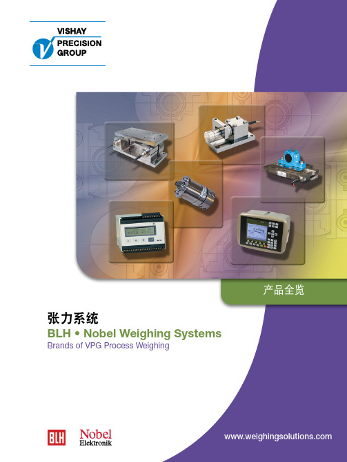
Vishay Nobel-kis1
- 格式:pdf
- 大小:142.27 KB
- 文档页数:4

文档编号:28832技术问题请联系 ************************具有优异耐潮能力的精密薄膜片式电阻阵列ACAS 0606 AT, ACAS 0612 AT - PrecisionVishay BeyschlagACAS 0606 AT 和ACAS 0612 AT 精密汽车级薄膜片式电阻阵列带有凸面端接,兼具分立片式电阻的可靠性和片式电阻阵列的诸多优点。
优异的容差匹配和TCR 跟踪,使这款产品极为适合对稳定的电阻比具有突出需求的应用。
ACAS 0612 AT 具有4个阻值相同的电阻或两对电阻,而ACAS 0606 AT 具有两个阻值相等或不同的电阻。
欲了解有关Vishay 汽车级产品要求的更多信息,请访问/applications 。
特性•优异的耐潮能力,|ΔR /R | < 0.5%(85 °C ;85 % RH ;1000小时)•每个电阻的额定耗散P 70高达125mW •ESD 保护为1000V ,人体模型•TCR 跟踪低至10ppm/K (±5ppm/K),容差匹配低至0.1% (±0.05%)•通过AEC-Q200认证•符合RoHS 指令2002/95/EC应用•精密模拟电路•分压器•反馈电路•信号调理注释(1)可以选E24~E96的阻值。
(2)在分压器或反馈电路等具有明确电阻比的应用中,要求使用具有10ppm/K 这样明确跟踪性能的阵列,替换阻值的温度系数为±5ppm/K 的分立式电阻。
而且,为了让每个独立电阻达到±0.05%的相同容差,要求阵列的匹配度达到0.1%。
(3)请参考应用信息。
技术规范说明单位ACAS 0606 ATACAS 0612 ATEIA 尺寸06060612公制尺寸RR 1616MM RR 1632M 结构,隔离的 2 x 0603 4 x 0603设计:所有电阻阻值相同(AE)AE AE 两对电阻阻值(TP)TP阻值不同(DF)DF阻值Ω47~150K (1)绝对容差%± 0.5; ± 0.25容差匹配 (2)%0.5 (相当于±0.25)0.25 (相当于±0.125)0.1 (相当于±0.05)绝对温度系数 ppm/K ± 50; ± 25温度系数跟踪 (2) ppm/K50 (相当于±25)25 (±12.5)15 (±7.5)10 (±5)最大电阻比 R min./R max.1:20额定耗散: P 70 (3)电阻芯W 0.1250.125封装0.20.4工作电压, U max . AC/DC V 75 允许薄膜温度°C 155对环境和集成电阻间的连续绝缘电压 (U ins ) V75 技术问题请联系 ************************文档编号:28832ACAS 0606 AT, ACAS 0612 AT - PrecisionVishay Beyschlag具有优异耐潮能力的精密薄膜片式电阻阵列应用信息电阻上的功率耗散会产生相对本地环境的温升,温度上升的幅度取决于印制电路板能够支持多大的热流(热阻)。

Sales Contacts Brands Interactive Guide 2200 SystemGain Controls: Continuously variable 1 to 3300. Gainpotentiometer 1.00 to 11.00 plus gain switch X1, X10, X100,X300.Filter Switch: Selects appropriate low-pass filter orwide-band operation.Monitor Jacks: For +10V output and bridge excitation.EXCIT LED: Denotes constant-voltage (red) orconstant-current (green) excitation.EXCIT On-Off: Toggle switch removes excitation from thestrain gage or transducer.EXCIT Potentiometer: Sets excitation level forconstant-voltage and constant-current excitation.CAL Switch: Selects A or B preset calibrationconfiguration.Auto BAL Switch: Controls balance operation.Auto BAL LED: Denotes balance mode: green during autobalance interval; red for overrange.Balance Trim Potentiometer: Refines bridge balance whendesirable.Balance LED: Indicates bridge balance (off), positiveunbalance (red), or negative unbalance (green).AMP Zero Potentiometer: Sets electrical zero of amplifier. SpecificationsAll references to microstrain assume a gage factor of 2.00.All specifications nominal or typical at +23 deg C unless noted.Input:Input Impedance:dc-coupled: 22 megohms shunted by 250 pF.ac-coupled: 1.1 microfarad in series with 20 kilohms; low frequency cutoff (3 dB) 8 Hz nom.Source Current:+10 nA typical; +20 nA maximum.Configuration:2- to 10-wire plus guard shield accepts quarter-, half-, or full-bridge strain gage or transducer inputs. Internal half-bridge, dummy 350 ohm and dummy 120 ohm completion gages, remote sense and four-wire calibration capability provided. 1000 ohms completion capability also provided. Accepts inputs from ground-referenced or isolated devices.Differential Input:Maximum differential input voltage of +50 Vdc or peak ac.Common-Mode Input:Maximum common-mode inputvoltage of +350 Vdc or peak ac.Guard Impedance:Greater than 250 kilohms to output common; greater than 1000 megohms to power and rack ground.Amplifier:Gain:1 to 3300; continuously variable; direct reading. Gain steps X1, X10, X100, X300; with 10-turn counting knob, X1 to X11. Accuracy +0.5%. Linearity:+0.01% of full scale at dc.Frequency Response:dc to 100 kHz: 3 +0.2 dB at all gain settings and full output. dc to 50 kHz: 0.5 dB max at all gain settings and full output.Gain Step vs Frequency Response (3 dB):X300100 kHzX100120 kHzX10135 kHzX1240 kHzSlew Rate:6.3 V/microsec min at all gain settings.Noise:(350 ohm source impedance, dc-coupled)Referred-to-input (RTI):1 microvolt 0.1 Hz to 10 Hz p-p;2 microvolts 0.1 Hz to 100 Hz p-p3 microvolts 0.1 Hz to 100 kHz rmsReferred-to-Output (RTO):Output related noise is a function of the setting of the gain multiplier potentiometer. Refer to the graph below for noise referred-to-output.Zero Stability:+2 microvolts RTI, +200 microvolts RTO at constant temp. Temperature Coefficient of Zero:+l microvolt/deg C RTI, +100 microvolt/deg C RTO; -10 deg to 60 deg C. Common-Mode Rejection:Gain CMR (dB)X182X10102X100122X300135Common-Mode Voltage:+350 Vdc or peak ac, max operating.Standard Output:+10V at 10 mA max;Tape Output:1.0 Vrms at 10 mA max; orOutput ac-coupled:+10V at 10 mA max (7 Hz, 3 dB).Output Monitor:+10V standard monitored via front-panel jacks.Output Isolation:>1000 megohms from power and rack ground.Output Protection:Protected against continuous short.Capacitive Loading:Up to 0.15 microfarad.Low-Pass Filter:Four-pole Bessel low-pass filter with selectable 3 dB bandwidths of 1 Hz, 10 Hz, 100 Hz, 1 kHz and 10 kHz.Constant-Voltage Excitation:Range:0.50 to 15.0 Vdc at 85 mA max.Noise:+100 microvolts +0.002% p-p dc to 20 kHz.Line Regulation:+200 microvolts +0.01 % max for line voltage change of 10% from nominal.Load Regulation:+200 microvolts +0.01% max for load variation of 10% to 90% of full load. Stability:+0.01%/deg C or 100 microvolts/deg C, whichever is greater.Remote Sense:Error <0.0005%/ohms of lead resistance.Monitoring:Front-panel monitoring jacks.Isolation:Isolated from power ground and output common; floats with guard. Constant-Current Excitation:Range:0.50 to 15.0 mA dc or 1.00 to 30.0 mA dc. Compliance voltage 0.50 to16.0V.Noise:(1 microamps + 10 microvolts) p-p; dc to 20 kHz.Line Regulation:+1 microamps +0.01% max for line voltage change of +10% from nominal. Load Regulation:+1 microamps +0.01% max for 100% load change.Stability:+0.01%/deg C or 1 microamp/deg C, whichever is greater.Monitoring:Front-panel monitoring jacks; 10 mV/mA.Isolation:Isolated from power ground and output common; floats with Guard. Balance:Method:Electronically injected automatic balance.Range:+15 000 microstrain (7.5 mV/V) RTI (X2 with internal jumper). Resolution:0.50/microstrain RTI (X2 with internal jumper).Balance Time:4 seconds typical; 8 seconds max.Accuracy:+2 mV RTO; +2 microstrain RTI.Balance Trim:+375 microstrain (188 microvolts/V) RTI.Storage:Digital with battery backup. Battery life 3-5 years.Activation:Activated by front-panel switch or by optically isolated remote switch or low TTL level.Calibration:Four internal shunt calibration resistors, +0.1% tolerance:174.8K 1000 microstrain (0.50 mV/V) 350 ohms bridge;874.8K 200 microstrain (0.10 mV/V) 350 ohms bridge;59.94K 1000 microstrain (0.50 mV/V) 120 ohms bridge. Activated by front-panel switch, or by optically isolated remote contact closure or low TTL level.Internal selector switches for selection of two-point unipolar, bipolar, or two-point double shunt calibration circuits.Calibration resistors plug into fixed terminals (no soldering).Size:7 H x 1.71 W x 17.88 D in (178 x 43 x 454 mm).Weight:3.7 lb (1.67 kg).Page 2 of 7。

ACASA1002S1002P1AT ACASN1002S1002P1AT ACASA1002S1002P1AT-DEL ACASN1002S1002P1AT-DELACAS 0606 AT, ACAS 0612 AT - PrecisionVishay BeyschlagPrecision Thin Film Chip Resistor ArraySuperior Moisture ResistivityACAS 0606 AT and ACAS 0612 AT precision automotive grade thin film chip resistor arrays with convex terminations combine the proven reliability of discrete chip resistors with the advantages of chip resistor arrays. D efined relative tolerance (matching) and relative TCR (tracking) make this product perfectly suited for applications with outstanding requirements towards stable fixed resistor ratios. The ACAS AT is available with equal or different resistor values. Find out more about Vishay’s automotive grade product requirements at: /applicationsFEATURES•Superior moisture resistivity, |∆R /R | < 0.5 % (85 °C; 85 % RH; 1000 h)•Rated dissipation P 70 up to 125 mW per resistor•ESD stability 1000 V, human body model •Relative TCR down to ± 5 ppm/K (tracking)•Relative tolerance down to ± 0.05 % (matching)•AEC-Q200 qualified•Material categorization: For definitions of compliance please see /doc?99912APPLICATIONS•Precision analogue circuits •Voltage divider •Feedback circuits •Signal conditioningNotes•The relative figures of tolerance, TCR and drift are related to a medial axis between the maximum and minimum permissable deviation of the resistor array. For detailed information please refer to the application note: Increasing Accuracy in Feedback Circuits and Voltage Dividers with Thin Film Chip Resistor Arrays (/doc?28194)(1)Resistance values to be selected from E24; E192.TECHNICAL SPECIFICATIONSDESCRIPTION ACAS 0606 ATACAS 0612 ATEIA size 06060612Metric sizeRR1616M RR1632M Configuration, isolated 2 x 06034 x 0603Design:All equal values (AE)AEAE Two pairs of values (TP)TPDifferent values (DF)DFResistance values 47 Ω to 150 k Ω (1)Absolute tolerance ± 0.1 %Relative tolerance± 0.05 %Absolute temperature coefficient ± 25 ppm/K; ± 15 ppm/K; ± 10 ppm/K Relative temperature coefficient ± 15 ppm/K; ± 10 ppm/K; ± 5 ppm/KMax. resistance ratio R min./R max.1:20Rated dissipation: P 70Element 0.125 W 0.125 W Package0.2 W0.4 WOperating voltage, U max . AC/DC 75 V Operating temperature range - 55 °C to 155 °CPermissible film temperature155 °C Insulation voltage (U ins ) against ambient and between integrated resistors, continuous75 VACAS 0606 AT, ACAS 0612 AT - PrecisionVishay BeyschlagAPPLICATION INFORMATIONThe power dissipation on the resistor generates a temperature rise against the local ambient, depending on the heat flow support of the printed-circuit board (thermal resistance). The rated dissipation applies only if the permitted film temperature is not exceeded. These resistors do not feature a limited lifetime when operated within the permissible limits.Note(1)Figures are given for arrays with equal values, design type AE.CIRCUITSMarking on ACAS 0606 AT: For types with different resistor values pin 1 is marked.MAXIMUM RESISTANCE CHANGE AT RATED POWER (1)DESCRIPTION ACAS 0606 AT ACAS 0612 AT Configuration, isolated 2 x 06034 x 0603Operation modeStandard Power Standard Power Rated power per element, P 700.1 W 0.125 W 0.1 W 0.125 W Rated power per package, P 700.15 W 0.2 W 0.3 W 0.4 W Film temperature125 °C155 °C125 °C155 °CMax. resistance change at P 70∆R /R max., after:1000 h± 0.1 %± 0.25 %± 0.1 %± 0.25 %8000 h± 0.25 %± 0.5 %± 0.25 %± 0.5 %Max. relative resistance change (relative drift) at P 70∆R /R max., after:1000 h ± 0.05 %± 0.125 %± 0.05 %± 0.125 %8000 h± 0.125 %± 0.25 %± 0.125 %± 0.25 %DESIGNACAS 0606 ATACAS 0612 AT AE R 1 = R 2R 1 = R 2 = R 3 = R 4TP R 1 = R 4 < R 2 = R 3DFR 1 < R 2ACAS 0606 AT, ACAS 0612 AT - PrecisionVishay BeyschlagNotes•Products can be ordered using either the PART NUMBER or the PRODUCT DESCRIPTION.(1)R 1 = R 4 ≤ R 2 = R 3.(2)For historical temperature coefficient and resistance ranges please refer to the end of the data sheet.Notes•For historical temperature coefficent and resistance range please refer to the end of the data sheet.•Relative TCR (tracking) down to ± 2.5 ppm/K on request.•Relative tolerance for resistance values < 80 Ω on request.PART NUMBER AND PRODUCT DESCRIPTIONPart Number: ACASA1100S2200P5ATMODEL/SIZE TERMINAL SIZE RESISTANCE (1)ACCURACY GRADE (2)RESISTANCE (1)PACKAGINGSpecial ACAS = Convex squareN = 0606A = 06123 digit resistance value R 1, R 41 digit multiplier TCR, Tracking, Tolerance and Matching S , T , or U3 digit resistance value R 2, R 31 digit multiplier P1P5AT = AutomotiveMULTIPLIER 9 = *10-10 = *1001 = *1012 = *1023 = *103MULTIPLIER 9 = *10-10 = *1001 = *1012 = *1023 = *103Product Description: ACAS 0612 110R S 220R AT P5ACA S 0612110R S 220R AT P5MODEL/SIZE TERMINAL SIZE RESISTANCE R 1, R 4 (1)ACCURACY GRADE (2)RESISTANCE R 2, R 3 (1)SPECIAL PACKAGINGACA = ChipArrayS = Convex square06060612110R = 110 Ω1K1 = 1.1 k Ω22K1 = 22.1 k ΩTCR, Tracking, Tolerance and Matching S , T , or U220R = 220 Ω1K1 = 1.1 k Ω22K1 = 22.1 k ΩAT = AutomotiveP1P5TEMPERATURE COEFFICIENT AND RESISTANCE RANGETYPEACCURACY GRADEABSOLUTE RELATIVERESISTANCEVALUE TCR TOLERANCE TCR TOLERANCE ACAS 0606 AT ACAS 0612 ATS± 25 ppm/K ± 0.1 %± 15 ppm/K ± 0.05 %47 Ω to 150 k ΩT ± 15 ppm/K ± 0.1 %± 10 ppm/K ± 0.05 %47 Ω to 150 k ΩU± 10 ppm/K± 0.1 %± 5 ppm/K± 0.05 %47 Ω to 100 k ΩS A 1100S 20C A A 205TP AACAS 0606 AT, ACAS 0612 AT - PrecisionVishay BeyschlagDIMENSIONSPATTERN STYLES FOR CHIP RESISTOR ARRAYSPACKAGINGTYPECODE QUANTITY PACKAGING STYLE WIDTHPITCHREEL DIAMETERACAS 0606 AT ACAS 0612 ATP11000Tape and reel cardboard tape acc. IEC 60286-3Type I8 mm 4 mm 180 mm/7"P55000DIMENSION AND MASSTYPEL (mm)W (mm)H (mm)P (mm)A 1(mm)A (mm)T 1(mm)T 2(mm)MASS (mg)ACAS 0606 AT 1.5 ± 0.15 1.6 ± 0.150.45 ± 0.1-0.6 ± 0.10.4 ± 0.10.3 ± 0.150.4 ± 0.15 3.6ACAS 0612 AT1.5 ± 0.153.2 ± 0.150.45 ± 0.10.8 ± 0.10.6 ± 0.10.4 ± 0.10.3 ± 0.150.4 ± 0.156.8RECOMMENDED SOLDER PAD DIMENSIONSTYPEG (mm)Y (mm)X (mm)U (mm)Z (mm)I (mm)P (mm)ACAS 0606 AT 0.70.70.64- 2.10.30.8ACAS 0612 AT0.70.70.640.52.10.30.8Dimensions in mmACAS 0606 AT, ACAS 0612 AT - Precision Vishay BeyschlagDESCRIPTIONThe production of the components is strictly controlled and follows an extensive set of instructions established for reproducibility. A homogeneous film of metal alloy is deposited on a high grade (Al2O3) ceramic substrate using a mask to separate the adjacent resistors and conditioned to achieve the desired temperature coefficient. Specially designed inner contacts are realized on both sides. A special laser is used to achieve the target value by smoothly cutting a meander groove in the resistive layer without damaging the ceramics.The resistor elements are covered by a protective coating designed for electrical, mechanical and climatic protection. The terminations receive a final pure tin on nickel plating. The result of the determined production is verified by an extensive testing procedure and optical inspection performed on 100 % of the individual chip resistors. Only accepted products are laid directly into the paper tape in accordance with IEC 60286-3(3).ASSEMBLYThe resistors are suitable for processing on automatic SMD assembly systems. They are suitable for automatic soldering using reflow or vapour phase as shown in IEC 61760-1(3). The encapsulation is resistant to all cleaning solvents commonly used in the electronics industry, including alcohols, esters and aqueous solutions.The suitability of conformal coatings, if applied, shall be qualified by appropriate means to ensure the long-term stability of the whole system. The resistors are RoHS compliant; the pure tin plating provides compatibility with lead (Pb)-free and lead-containing soldering processes. The permitted storage time is 20 years, whereas the solderability is specified for 2 years after production or requalification. The immunity of the plating against tin whisker growth has been proven under extensive testing.All products comply with the GADSL (1) and the CEFIC-EECA-EICTA (2) list of legal restrictions on hazardous substances. This includes full compliance with the following directives:•2000/53/EC End of Life Vehicle D irective (ELV) and Annex II (ELV II)•2011/65/EC Restriction of the use of Hazardous Substances directive (RoHS)•2002/96/EC Waste Electrical and Electronic Equipment Directive (WEEE)APPROVALSThe chip resistor array is AEC-Q200 qualified.Where applicable, the resistors are tested in accordance with EN 140401-801 which refers to EN 60115-1 and EN 140400.Notes(1)Global Automotive Declarable Substance List, see .(2)CEFIC (European Chemical Industry Council), EECA (European Electronic Component Manufacturers Association), EICTA (European tradeorganisation representing the information and communications technology and consumer electronics), see → policy →environmental policy group → chemicals → jig → Joint Industry Guide (JIG-101 Ed 2.0).(3)The quoted IEC standards are also released as EN standards with the same number and identical contents.FUNCTIONAL PERFORMANCEACAS 0606 AT, ACAS 0612 AT - Precision Vishay BeyschlagTESTS AND REQUIREMENTSEssentially all tests are carried out in accordance with the following specifications:EN 60115-1, generic specificationEN 140400, sectional specificationEN 140401-801, detail specificationThe testing also covers most of the requirements specified by EIA/IS-703 and JIS-C-5202.The tests are are carried out under standard atmospheric conditions according to IEC 60068-1 (1), 5.3. Climatic category LCT/UCT/56 (rated temperature range: Lower category temperature, upper category temperature; damp heat, long term, 56 days) is valid (LCT = - 55 °C/ UCT = 125 °C).Unless otherwise specified the following values apply: Temperature: 15 °C to 35 °CRelative humidity: 45 % to 75 %Air pressure: 86 kPa to 106 kPa (860 mbar to 1060 mbar) The requirements stated in the “Test Procedures and Requirements” table are based on the required tests and permitted limits of EN 140401-801 where applicable.TEST PROCEDURES AND REQUIREMENTSEN 60 115-1 CLAUSEIEC60 068-2 (1)TESTMETHODTEST PROCEDUREREQUIREMENTSPERMISSIBLE CHANGE (2)(∆R)Stability for product types:ACAS 0606 ATACAS 0612 AT47 Ω to 150 kΩ47 Ω to 150 kΩ4.5-Resistance-± 0.1 %4.8.4.2-Temperature coefficient At (20/- 55/ 20) °C and(20/125/20) °C± 25 ppm/K; ± 15 ppm/K; ± 10 ppm/K4.25.1-Endurance at 70 °C:Standard operation modeU =or U = U max.;1.5 h on; 0.5 h off;whichever is the less severe;1000 h:AbsoluteRelative± (0.1 % R + 0.05 Ω)± (0.05 % R + 0.05 Ω)8000 h:AbsoluteRelative± (0.25 % R + 0.05 Ω)± (0.125 % R + 0.05 Ω)Endurance at 70 °C:Power operation modeU =or U = U max.;1.5 h on; 0.5 h off;whichever is the less severe;1000 h:AbsoluteRelative± (0.25 % R + 0.05 Ω)± (0.125 % R + 0.05 Ω)8000 h:AbsoluteRelative± (0.5 % R + 0.05 Ω)± (0.25 % R + 0.05 Ω)4.25.3-Endurance at uppercategory temperature125 °C; 1000 h:AbsoluteRelative± (0.25 % R + 0.05 Ω)± (0.125 % R + 0.05 Ω)125 °C; 8000 h:AbsoluteRelative± (0.5 % R + 0.05 Ω)± (0.25 % R + 0.05 Ω)155 °C; 1000 h:AbsoluteRelative± (0.4 % R + 0.05 Ω)± (0.2 % R + 0.05 Ω)4.2478 (Cab)Damp heat,steady state(40 ± 2) ︒C; 56 days;(93 ± 3) % RH± (0.25 % R + 0.05 Ω)4.3967 (Cy)Damp heat,steady state,accelerated(85 ± 2) °C(85 ± 5) % RHU = ;U≤ 0.3 x U max.;1000 h± (0.5 % R + 0.05 Ω)P70 x RP70 x R0.1 x P70x RACAS 0606 AT, ACAS 0612 AT - PrecisionVishay BeyschlagNotes(1)The quoted IEC standards are also released as EN standards with the same number and identical contents.(2)Figures are given for arrays with equal values, design type AE.(3)For a single element.Note•Special temperature coefficent and resistance combinations remain available. For optimized availability please refer to the table TEMPERATURE COEFFICENT AND RESISTANCE.4.13-Short time overload (3)Standard operation mode U = 2.5 x orU = 2 x U max.;5 s± (0.1 % R + 0.01 Ω)no visible damage 4.40-Electrostatic discharge (human body model) (3)IEC 61340-3-1;3 pos. + 3 neg.(equivalent to MIL-STD-883, Method 3015); 1000 V ± (0.5 % R + 0.05 Ω)4.1914 (Na)Rapid change of temperature 30 min at - 55 °C and 30 min at 125 °C;1000 cycles ± (0.25 % R + 0.05 Ω)no visible damage 4.18.258 (Td)Resistance to solderingheatReflow method 2 (IR/forced gas convection);(260 ± 5) ︒C; (10 ± 1) s± (0.1 % R + 0.01 Ω)no visible damage 4.17.258 (Td)SolderabilitySolder bath method;SnPb; non-activated flux accelerated aging 4 h/155 °C (215 ± 3) °C; (3 ± 0.3) s Good tinning (≥ 95 % covered);no visible damageSolder bath method;SnAgCu; non-activated flux accelerated aging 4 h/155 °C (235 ± 3) °C; (2 ± 0.2) s4.3221 (Ue 3)Shear (adhesion)45 NNo visible damage 4.3321 (Ue 1)Substrate bending Depth 2 mm, 3 times ± (0.1 % R + 0.01 Ω)no visible damage;no open circuit in bent position4.35-Flammability IEC 60695-11-5, needle flame test; 10 s No burning after 30 s 4.226 (Fc)VibrationEndurance by sweeping;10 Hz to 2000 Hz; no resonance;amplitude ≤ 1.5 mm or ≤ 200 m/s 2; 7.5 h ± (0.1 % R + 0.01 Ω)no visible damage 4.7-Voltage proofU RMS = U ins60 s ± 5 s; against ambient, between adjacent resistorsNo flashover or breakdownHISTORICAL TEMPERATURE COEFFICIENT AND RESISTANCE RANGESDESCRIPTIONRESISTANCE VALUEACCURACY GRADEABSOLUTE TCR TCR TRACKINGABSOLUTE TOLERANCE TOLERANCE MATCHINGACAS 0606 AT ACAS 0612 AT A ± 25 ppm/K 10 ppm/K ± 0.25 %0.1 %47 Ω to 150 k ΩB ± 25 ppm/K 10 ppm/K ± 0.5 %0.25 %47 Ω to 150 k ΩE ± 25 ppm/K 15 ppm/K ± 0.25 %0.1 %47 Ω to 150 k ΩF ± 25 ppm/K 15 ppm/K ± 0.5 %0.25 %47 Ω to 150 k ΩJ ± 25 ppm/K 25 ppm/K ± 0.25 %0.1 %47 Ω to 150 k ΩK ± 25 ppm/K 25 ppm/K ± 0.5 %0.25 %47 Ω to 150 k ΩN ± 50 ppm/K 25 ppm/K ± 0.5 %0.5 %47 Ω to 150 k ΩP± 50 ppm/K50 ppm/K± 0.5 %0.5 %47 Ω to 150 k ΩTEST PROCEDURES AND REQUIREMENTSEN 60 115-1CLAUSEIEC 60 068-2 (1)TEST METHODTESTPROCEDUREREQUIREMENTSPERMISSIBLE CHANGE (2)(∆R )Stability for product types:ACAS 0606 AT ACAS 0612 AT47 Ω to 150 k Ω47 Ω to 150 k ΩP 70 x RLegal Disclaimer Notice VishayDisclaimerALL PRODUCT, PRODUCT SPECIFICAT IONS AND DAT A ARE SUBJECT T O CHANGE WIT HOUT NOT ICE T O IMPROVE RELIABILITY, FUNCTION OR DESIGN OR OTHERWISE.Vishay Intertechnology, Inc., its affiliates, agents, and employees, and all persons acting on its or their behalf (collectively, “Vishay”), disclaim any and all liability for any errors, inaccuracies or incompleteness contained in any datasheet or in any other disclosure relating to any product.Vishay makes no warranty, representation or guarantee regarding the suitability of the products for any particular purpose or the continuing production of any product. To the maximum extent permitted by applicable law, Vishay disclaims (i) any and all liability arising out of the application or use of any product, (ii) any and all liability, including without limitation special, consequential or incidental damages, and (iii) any and all implied warranties, including warranties of fitness for particular purpose, non-infringement and merchantability.Statements regarding the suitability of products for certain types of applications are based on Vishay’s knowledge of typical requirements that are often placed on Vishay products in generic applications. Such statements are not binding statements about the suitability of products for a particular application. It is the customer’s responsibility to validate that a particular product with the properties described in the product specification is suitable for use in a particular application. Parameters provided in datasheets and / or specifications may vary in different applications and performance may vary over time. All operating parameters, including typical parameters, must be validated for each customer application by the customer’s technical experts. Product specifications do not expand or otherwise modify Vishay’s terms and conditions of purchase, including but not limited to the warranty expressed therein.Except as expressly indicated in writing, Vishay products are not designed for use in medical, life-saving, or life-sustaining applications or for any other application in which the failure of the Vishay product could result in personal injury or death. Customers using or selling Vishay products not expressly indicated for use in such applications do so at their own risk. Please contact authorized Vishay personnel to obtain written terms and conditions regarding products designed for such applications.No license, express or implied, by estoppel or otherwise, to any intellectual property rights is granted by this document or by any conduct of Vishay. Product names and markings noted herein may be trademarks of their respective owners.© 2017 VISHAY INTERTECHNOLOGY, INC. ALL RIGHTS RESERVEDACASA1002S1002P1AT ACASN1002S1002P1AT ACASA1002S1002P1AT-DEL ACASN1002S1002P1AT-DEL。
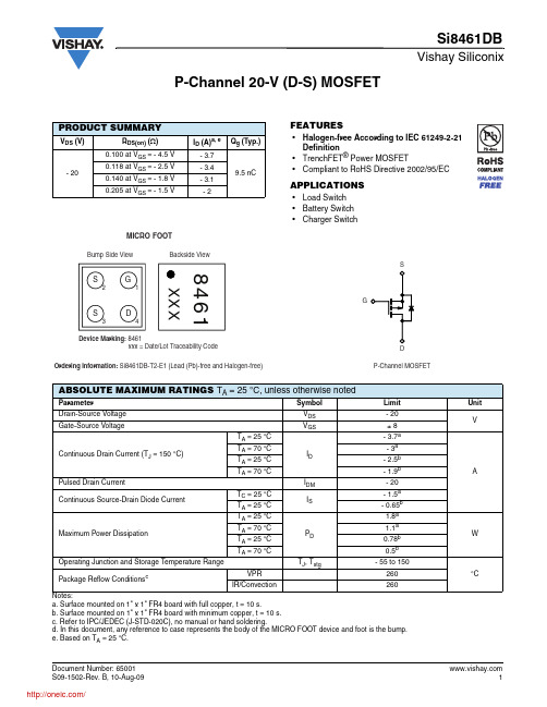
Vishay SiliconixSi8461DBDocument Number: P-Channel 20-V (D-S) MOSFETFEATURES•Halogen-free According to IEC 61249-2-21Definition•TrenchFET ® Power MOSFET•Compliant to RoHS Directive 2002/95/ECAPPLICATIONS•Load Switch •Battery Switch •Charger SwitchNotes:a. Surface mounted on 1" x 1" FR4 board with full copper, t = 10 s.b. Surface mounted on 1" x 1" FR4 board with minimum copper, t = 10 s.c. Refer to IPC/JEDEC (J-STD-020C), no manual or hand soldering.d. In this document, any reference to case represents the body of the MICRO FOOT device and foot is the bump.e. Based on T A = 25 °C.PRODUCT SUMMARYV DS (V)R DS(on) (Ω)I D (A)a, e Q g (Typ.)- 200.100 at V GS = - 4.5 V- 3.79.5 nC 0.118 at V GS = - 2.5 V - 3.40.140 at V GS = - 1.8 V - 3.10.205 at V GS = - 1.5 V- 2ABSOLUTE MAXIMUM RATINGS T A = 25°C, unless otherwise notedParameter Symbol Limit UnitDrain-Source Voltage V DS - 20VGate-Source VoltageV GS± 8Continuous Drain Current (T J = 150 °C)T A = 25 °CI D - 3.7a A T A = 70 °C - 3a T A = 25 °C - 2.5b T A = 70 °C- 1.9b Pulsed Drain CurrentI DM - 20Continuous Source-Drain Diode CurrentT C = 25 °C I S - 1.5a T A = 25 °C - 0.65b Maximum Power DissipationT A = 25 °CP D 1.8a W T A = 70 °C 1.1a T A = 25 °C 0.78b T A = 70 °C0.5b Operating Junction and Storage Temperature Range T J , T stg - 55 to 150°C Package Reflow Conditions cVPR 260IR/Convection260 Document Number: 65001Vishay SiliconixSi8461DBNotes:a. Surface mounted on 1" x 1" FR4 board with full copper.b. Maximum under steady state conditions is 100 °C/W.c. Surface mounted on 1" x 1" FR4 board with minimum copper.d. Maximum under steady state conditions is 190 °C/W.THERMAL RESISTANCE RATINGSParameter Symbol Typical Maximum UnitMaximum Junction-to-Ambient a, b t = 10 s R thJA5570°C/WMaximum Junction-to-Ambient c, dt = 10 s125160SPECIFICATIONS T J = 25°C, unless otherwise notedParameter Symbol Test Conditions Min.Typ.Max.UnitStaticDrain-Source Breakdown Voltage V DS V GS = 0 V , I D = - 250 µA- 20V V DS Temperature Coefficient ΔV DS /T J I D = - 250 µA - 12mV/°C V GS(th) Temperature Coefficient ΔV GS(th)/T J 2.5Gate-Source Threshold Voltage V GS(th) V DS = V GS , I D = - 250 µA - 0.4- 1.0V Gate-Source LeakageI GSS V DS = 0 V, V GS = ± 8 V ± 100nA Zero Gate Voltage Drain Current I DSS V DS = - 20 V , V GS = 0 V - 1µA V DS = - 20 V , V GS = 0 V , T J = 70 °C- 10On-State Drain Current aI D(on)V DS ≤ - 5 V , V GS = - 4.5 V - 10ADrain-Source On-State Resistance aR DS(on)V GS = - 4.5 V , I D = - 1.5 A0.0830.100ΩV GS = - 2.5 V , I D = - 1.5 A 0.0980.118V GS = - 1.8 V , I D = - 1 A 0.1150.140V GS = - 1.5 V , I D = - 0.5 A0.1360.205Forward T ransconductance a g fsV DS = - 10 V , I D = - 1 A7S Dynamic bInput Capacitance C iss V DS = - 10 V , V GS = 0 V, f = 1 MHz610pFOutput CapacitanceC oss 120Reverse Transfer Capacitance C rss 95Total Gate Charge Q g V DS = - 10 V , V GS = - 8 V , ID = - 1 A 1624nC V DS = - 10 V , V GS = - 4.5 V, I D = 1 A 9.515Gate-Source Charge Q gs 0.9Gate-Drain Charge Q gd 2.6Gate Resistance R g V GS = - 0.1 V , f = 1 MHz 6.5ΩTurn-On Delay Time t d(on) V DD = - 10 V, R L = 10 Ω I D ≅ - 1 A, V GEN = - 4.5 V , R g = 1 Ω1525ns Rise Timet r 2540Turn-Off Delay Time t d(off) 3555Fall Timet f 1015Turn-On Delay Time t d(on) V DD = - 10 V, R L = 10 ΩI D ≅ - 1 A, V GEN = - 8 V, R g = 1 Ω715Rise Timet r 1220Turn-Off Delay Time t d(off) 3250Fall Timet f1220Document Number: Vishay SiliconixSi8461DBNotes:a. Pulse test; pulse width ≤ 300 µs, duty cycle ≤ 2 %.b. Guaranteed by design, not subject to production testing.Stresses beyond those listed under “Absolute Maximum Ratings” may cause permanent damage to the device. These are stress ratings only, and functional operation of the device at these or any other conditions beyond those indicated in the operational sections of the specifications is not implied. Exposure to absolute maximum rating conditions for extended periods may affect device reliability.SPECIFICATIONS T J = 25°C, unless otherwise notedParameter Symbol Test Conditions Min.Typ.Max.UnitDrain-Source Body Diode Characteristics Continuous Source-Drain Diode Current I S T A = 25 °C- 1.5A Pulse Diode Forward Current I SM - 20Body Diode VoltageV SD I S = - 1 A, V GS = 0 V- 0.8- 1.2V Body Diode Reverse Recovery Time t rr I F = - 1 A, dI/dt = 100 A/µs, T J = 25 °C1530ns Body Diode Reverse Recovery Charge Q rr 1020nC Reverse Recovery Fall Time t a 9nsReverse Recovery Rise Timet b6 Document Number: 65001Gate ChargeOn-Resistance vs. Junction TemperatureSi8461DBVishay Siliconix TYPICAL CHARACTERISTICS 25Safe Operating Area, Junction-to-AmbientDocument Number: Document Number: 65001Vishay SiliconixSi8461DBTYPICAL CHARACTERISTICS 25°C, unless otherwise notedNote:When Mounted on 1" x 1" FR4 with Full Copper.* The power dissipation P D is based on T J(max) = 150 °C, using junction-to-case thermal resistance, and is more useful in settling the upper dissipation limit for cases where additional heatsinking is used. It is used to determine the current rating, when this rating falls below the package limit.Current Derating*Power DeratingSi8461DBVishay Siliconix TYPICAL CHARACTERISTICS 25°C, unless otherwise notedNormalized Thermal Transient Impedance, Junction-to-Ambient (1" x 1" FR4 Board with Full Copper)Document Number: Document Number: 65001Vishay SiliconixSi8461DBPACKAGE OUTLINEMICRO FOOT: 4-BUMP (2 x 2, 0.5 mm PITCH)Notes (Unless otherwise specified):1. All dimensions are in millimeters.2. Four (4) solder bumps are lead (Pb)-free 95.5Sn/3.8Ag/0.7Cu with diameter ∅ 0.30 mm to 0.32 mm.3. Backside surface is coated with a Ti/Ni/Ag layer.4. Non-solder mask defined copper landing pad.5. • is location of pin 1.Notes:a. Use millimeters as the primary measurement.Vishay Siliconix maintains worldwide manufacturing capability. Products may be manufactured at one of several qualified locations. Reliability data for Silicon Technology and Package Reliability represent a composite of all qualified locations. For related documents such as package/tape drawings, part marking, and reliability data, see /ppg?65001.Dim. Millimeters aInches Min. Nom.Max. Min. Nom.Max. A 0.4620.5050.5480.01810.01980.0215A 1 0.2200.2500.2800.00860.00980.0110A 2 0.2420.2550.2680.00950.01000.0105b 0.3000.3100.3200.01180.01220.0126e 0.5000.0197s 0.2300.2500.2700.00900.00980.0106D0.9200.9601.0000.03620.03780.0394Legal Disclaimer Notice VishayDisclaimerALL PRODU CT, PRODU CT SPECIFICATIONS AND DATA ARE SU BJECT TO CHANGE WITHOU T NOTICE TO IMPROVE RELIABILITY, FUNCTION OR DESIGN OR OTHERWISE.Vishay Intertechnology, Inc., its affiliates, agents, and employees, and all persons acting on its or their behalf (collectively,“Vishay”), disclaim any and all liability for any errors, inaccuracies or incompleteness contained in any datasheet or in any other disclosure relating to any product.Vishay makes no warranty, representation or guarantee regarding the suitability of the products for any particular purpose or the continuing production of any product. To the maximum extent permitted by applicable law, Vishay disclaims (i) any and all liability arising out of the application or use of any product, (ii) any and all liability, including without limitation special, consequential or incidental damages, and (iii) any and all implied warranties, including warranties of fitness for particular purpose, non-infringement and merchantability.Statements regarding the suitability of products for certain types of applications are based on Vishay’s knowledge of typical requirements that are often placed on Vishay products in generic applications. Such statements are not binding statements about the suitability of products for a particular application. It is the customer’s responsibility to validate that a particular product with the properties described in the product specification is suitable for use in a particular application. Parameters provided in datasheets and/or specifications may vary in different applications and performance may vary over time. All operating parameters, including typical parameters, must be validated for each customer application by the customer’s technical experts. Product specifications do not expand or otherwise modify Vishay’s terms and conditions of purchase, including but not limited to the warranty expressed therein.Except as expressly indicated in writing, Vishay products are not designed for use in medical, life-saving, or life-sustaining applications or for any other application in which the failure of the Vishay product could result in personal injury or death. Customers using or selling Vishay products not expressly indicated for use in such applications do so at their own risk and agree to fully indemnify and hold Vishay and its distributors harmless from and against any and all claims, liabilities, expenses and damages arising or resulting in connection with such use or sale, including attorneys fees, even if such claim alleges that Vishay or its distributor was negligent regarding the design or manufacture of the part. Please contact authorized Vishay personnel to obtain written terms and conditions regarding products designed for such applications.No license, express or implied, by estoppel or otherwise, to any intellectual property rights is granted by this document or by any conduct of Vishay. Product names and markings noted herein may be trademarks of their respective owners.Material Category PolicyVishay Intertechnology, Inc. hereb y certifies that all its products that are identified as RoHS-Compliant fulfill the definitions and restrictions defined under Directive 2011/65/EU of The European Parliament and of the Council of June 8, 2011 on the restriction of the use of certain hazardous substances in electrical and electronic equipment (EEE) - recast, unless otherwise specified as non-compliant.Please note that some Vishay documentation may still make reference to RoHS Directive 2002/95/EC. We confirm that all the products identified as being compliant to Directive 2002/95/EC conform to Directive 2011/65/EU.Revision: 12-Mar-121Document Number: 91000分销商库存信息: VISHAYSI8461DB-T2-E1。

1 Form A Solid-State RelayDESCRIPTIONThe VOR1142 is an SPST normally open switch (1 form A) that can replace electromechanical relays in many applications. It is constructed using a GaAlAs IRED actuation control and MOSFETs for the switch output.FEATURES•Current limit protection•Isolation test voltage 3750 V RMS•Typical R ON 22 Ω•Load voltage 400 V•Load current 140 mA•High surge capability•Clean bounce free switching•Low power consumption•High temperature range•Material categorization: for definitions of compliance please see /doc?99912 APPLICATIONS•General telecom switching•Metering•Security equipment•Instrumentation•Industrial controls•Battery management systems•Automatic measurement equipmentAGENCY APPROVALS•UL1577, file no. E52744•DIN EN 60747-5-5 (VDE0884-5)Notes•Stresses in excess of the absolute maximum ratings can cause permanent damage to the device. Functional operation of the device is not implied at these or any other conditions in excess of those given in the operational sections of this document. Exposure to absolute maximum ratings for extended periods of the time can adversely affect reliability.(1)For continuous negative potential from output side to input side only 85 °C is allowed.Note•Minimum and maximum values are testing requirements. Typical values are characteristics of the device and are the result of engineering evaluations. Typical values are for information only and are not part of the testing requirements.ABSOLUTE MAXIMUM RATINGS (T amb = 25 °C, unless otherwise specified)PARAMETER CONDITIONSSYMBOLVALUE UNIT INPUTIRED continuous forward current I F 50mA IRED reverse voltage V R 5V Input power dissipation P diss 80mW OUTPUTDC or peak AC load voltage V L 400V Continuous DC load current I L 140mA SSR output power dissipation P diss 550mW SSRAmbient temperature range (1)T amb -40 to +100°C Storage temperature range T stg-40 to +150°C Soldering temperaturet = 10 s max.T sld260°CELECTRICAL CHARACTERISTICS (T amb = 25 °C, unless otherwise specified)PARAMETER TEST CONDITIONSYMBOLMIN.TYP.MAX.UNITINPUTIRED forward current, switch turn-on I L = 100 mA, t = 10 ms I Fon -0.252mA IRED forward current, switch turn-off V L = ± 350 V, I L < 1 μAI Foff 0.050.15-mA IRED forward voltage I F = 10 mA V F - 1.36 1.5V IRED reverse current V R = 5 VI R--10μAOUTPUT On-resistance I F = 5 mA, I L = 50 mA R ON -2227ΩOff-resistanceI F = 0 mA, V L = ± 100 V R OFF 0.5850-G ΩOff-state leakage current I F = 0 mA, V L = ± 100 V I leak -< 1100nA I F = 0 mA, V L = ± 400 V I leak -6500nA Output capacitance I F = 0 mA, V L = 1 V, 1 MHz C O -39-pF I F = 0 mA, V L = 50 V, 1 MHz C O -6-pF Current limit AC/DC I F = 5 mA, t = 5 ms, V L = ± 6 VI limit170300450mACOUPLERCapacitance (input to output)V IO = 1 VC IO-0.4-pFFig. 1 - Timing SchematicNote•As per IEC 60747-5-5, §7.4.3.8.2, this optocoupler is suitable for “safe electrical insulation” only within the safety ratings. Compliance with the safety ratings shall be ensured by means of protective circuits.SWITCHING CHARACTERISTICS (T amb = 25 °C, unless otherwise specified)PARAMETER TEST CONDITION SYMBOLMIN.TYP.MAX.UNIT Turn-on time I F = 5 mA, I L = 50 mA t on -0.20.5ms Turn-off timeI F = 5 mA, I L = 50 mAt off-0.050.2msSAFETY AND INSULATION RATINGSPARAMETER TEST CONDITION SYMBOLVALUE UNITClimatic classification According to IEC 68 part 140/100/21Pollution degreeAccording to DIN VDE 01092Comparative tracking indexCTI 175Maximum rated withstanding isolation voltage According to UL1577, t = 1 min V ISO 3750V RMS Maximum transient isolation voltage According to DIN EN 60747-5-5V IOTM 6000V peak Maximum repetitive peak isolation voltage According to DIN EN 60747-5-5V IORM 707V peak Isolation resistance T amb = 25 °C, V IO = 500 V R IO ≥ 1012ΩT amb = 100 °C, V IO = 500 VR IO ≥ 1011ΩOutput safety power P SO 550mW Input safety current I SI 180mA Input safety temperature T S 175°CClearance distance SOP-4≥ 5mm Creepage distance SOP-4≥ 5mm Insulation thicknessDTI ≥ 0.3mm Input to output test voltage, method B V IORM x 1.875 = V PR , 100 % production test with t M = 1 s, partial discharge < 5 pC V PR 1326V peak Input to output test voltage, method AV IORM x 1.6 = V PR , sample test with t M = 10 s,partial discharge < 5 pCV PR1131V peakFig. 2 - Safety Input Current vs. Ambient TemperatureFig. 3 - Safety Power Dissipation vs. Ambient TemperatureTYPICAL CHARACTERISTICS (T amb = 25 °C, unless otherwise specified)Fig. 4 - Maximum Load Current vs. Ambient TemperatureFig. 5 - Forward Voltage vs. Ambient TemperatureFig. 6 - Forward Current vs. Forward VoltageFig. 7 - Normalized Forward Current for Switch Turn-On vs.Ambient TemperatureFig. 8 - Normalized On-Resistance vs. Ambient Temperature Fig. 9 - Output Capacitance vs. Load Voltage Fig. 10 - Off-State Leakage Current vs. Load VoltageFig. 11 - Turn-On Time vs. Forward CurrentFig. 12 - Normalized Turn-On Time vs. Ambient Temperature Fig. 13 - Turn-Off Time vs. Forward CurrentFig. 14 - Normalized Turn-Off Time vs. Ambient TemperaturePACKAGE DIMENSIONS (in millimeters)Fig. 15 - Package DrawingPACKAGE MARKINGFig. 16 - VOR1142M4Note•Package configuration (T, M) are not part of the package marking.PACKAGING INFORMATION (in millimeters)Fig. 17 - Tape and Reel Packing (2000 pieces on reel)SOLDER PROFILESFig. 18 - Lead (Pb)-free Reflow Solder Profile According toJ-STD-020 for SMD DevicesHANDLING AND STORAGE CONDITIONSESD level: HBM class 2Floor life: unlimitedConditions: T amb < 30 °C, RH < 85 %Moisture sensitivity level 1, according to J-STD-020DEVICE PER TUBETYPE UNITS/TUBETUBES/BOXUNITS/BOXSOP-4100404000Legal Disclaimer Notice VishayDisclaimerALL PRODUCT, PRODUCT SPECIFICAT IONS AND DAT A ARE SUBJECT T O CHANGE WIT HOUT NOT ICE T O IMPROVE RELIABILITY, FUNCTION OR DESIGN OR OTHERWISE.Vishay Intertechnology, Inc., its affiliates, agents, and employees, and all persons acting on its or their behalf (collectively, “Vishay”), disclaim any and all liability for any errors, inaccuracies or incompleteness contained in any datasheet or in any other disclosure relating to any product.Vishay makes no warranty, representation or guarantee regarding the suitability of the products for any particular purpose or the continuing production of any product. To the maximum extent permitted by applicable law, Vishay disclaims (i) any and all liability arising out of the application or use of any product, (ii) any and all liability, including without limitation special, consequential or incidental damages, and (iii) any and all implied warranties, including warranties of fitness for particular purpose, non-infringement and merchantability.Statements regarding the suitability of products for certain types of applications are based on Vishay’s knowledge of typical requirements that are often placed on Vishay products in generic applications. Such statements are not binding statements about the suitability of products for a particular application. It is the customer’s responsibility to validate that a particular product with the properties described in the product specification is suitable for use in a particular application. Parameters provided in datasheets and / or specifications may vary in different applications and performance may vary over time. All operating parameters, including typical parameters, must be validated for each customer application by the customer’s technical experts. Product specifications do not expand or otherwise modify Vishay’s terms and conditions of purchase, including but not limited to the warranty expressed therein.Except as expressly indicated in writing, Vishay products are not designed for use in medical, life-saving, or life-sustaining applications or for any other application in which the failure of the Vishay product could result in personal injury or death. Customers using or selling Vishay products not expressly indicated for use in such applications do so at their own risk. Please contact authorized Vishay personnel to obtain written terms and conditions regarding products designed for such applications.No license, express or implied, by estoppel or otherwise, to any intellectual property rights is granted by this document or by any conduct of Vishay. Product names and markings noted herein may be trademarks of their respective owners.© 2017 VISHAY INTERTECHNOLOGY, INC. ALL RIGHTS RESERVED。
R e fl e c ti v eS e ns o r sW i t hA n a l o gO u tp u tT r i p l e an dQ u ad C ha n ne lT r a n s mi s s iv e Se n so r sA m b i e nt L i gh t Se n so r sW i t hA n a l o ga n dD i gi t a lO u tp u tI n t e g r at e dP r ox i mi t y an db i en t Li g h tS e ns o r sW i t hu t pu tS e ns o r sW i t hA n al o gO u tp u tI n t eg r at e dM ul t i pl e Ba n dS e ns o r sS i ng l ea n dD u alC h an n el T ra n sm i ss i v eS e ns o r sH i gh Re s ol u t io n Se n so r sf o rU V Aa n dU V BM e as u r em e nt sU VS E NS O RST C XT13X0X01C O LO RS E NS O RST R AN S MI S S IV ES E NS O RSV C NL F AM I LYA M BI E NT L IG H TS E NS O RST C UT1630X01T C UT1800X01R E FL E CT I V ES E NS O RSNotes: (1) All optical sensors have phototransistor output except where noted (2) Relative collector current > 20 % (3) TCND5000 has a PIN photodiode outputNotes: (1) All optical sensors have phototransistor output (2) Dual channel (3) Triple channel (4) Quad channel (5) Products ending in “X01” are AEC-Q101 qualified(1)1206, SMD 5 mm, flat top5 mm 3 mmNotes: (1) E v = 100 lux, V CE = 5 V , CIE illuminant A, typical (2)Products ending in “X01” are AEC-Q101 qualifiedPackageNotes:(1)Products ending in “X01” are AEC-Q101 qualifiedNo matter what car you drive,optical sensors are close by.Think automotive, think Vishay! Vishay’s proximity, reflective,transmissive, and ambient lightsensors put the “smart” intosmart devices with best-in-class performanceUseful Links • Optical Sensors gateway/optical-sensors/• Transmissive Sensors infograph/doc?48352• Proximity Sensors infograph/doc?49820• Current Estimator calculator/optoelectronics/opto-sensors-calculator/• Vishay Automotive Grade Optoelectronics selector guide /doc?49071• Sensor starter kit/moreinfo/SensorXplorer/。
Document Number: 91054 Power MOSFETIRF740, SiHF740Vishay SiliconixFEATURES•Dynamic dV/dt Rating •Repetitive Avalanche Rated •Fast Switching •Ease of Paralleling •Simple Drive Requirements•Compliant to RoHS Directive 2002/95/ECDESCRIPTIONThird generation Power MOSFETs from Vishay provide the designer with the best combination of fast switching,ruggedized device design, low on-resistance and cost-effectiveness.The TO-220AB package is universally preferred for all commercial-industrial applications at power dissipation levels to approximately 50 W. The low thermal resistance and low package cost of the TO-220AB contribute to its wide acceptance throughout the industry.Notesa.Repetitive rating; pulse width limited by maximum junction temperature (see fig. 11).b.V DD = 50 V, starting T J = 25 °C, L = 9.1 mH, R g = 25 Ω, I AS = 10 A (see fig. 12).c.I SD ≤ 10 A, dI/dt ≤ 120 A/μs, V DD ≤ V DS , T J ≤ 150 °C.d. 1.6 mm from case.PRODUCT SUMMARYV DS (V)400R DS(on) (Ω)V GS = 10 V0.55Q g (Max.) (nC)63Q gs (nC)9.0Q gd (nC)32ConfigurationSingleTO-220ABGDSORDERING INFORMATIONPackage TO-220AB Lead (Pb)-free IRF740PbF SiHF740-E3 SnPbIRF740SiHF740ABSOLUTE MAXIMUM RATINGS (T C = 25 °C, unless otherwise noted)PA AMETE SYMBOL LIMIT UNIT Drain-Source Voltage V DS 400VGate-Source Voltage V GS ± 20Continuous Drain Current V GS at 10 VT C = 25 °C I D10A T C = 100 °C6.3Pulsed Drain Current a I DM 40Linear Derating Factor1.0W/°C Single Pulse Avalanche Energy b E AS 520mJ Repetitive Avalanche Current a I AR 10 A Repetitive Avalanche Energy a E AR 13mJ Maximum Power Dissipation T C = 25 °CP D 125WPeak Diode Recovery dV/dt cdV/dt 4.0V/ns Operating Junction and Storage Temperature Range T J , T stg- 55 to + 150°C Soldering Recommendations (Peak Temperature)for 10 s 300d Mounting Torque6-32 or M3 screw10 lbf · in1.1N · m* Pb containing terminations are not RoHS compliant, exemptions may applyDocument Number: 91054IRF740, SiHF740Vishay SiliconixNotesa.Repetitive rating; pulse width limited by maximum junction temperature (see fig. 11).b.Pulse width ≤ 300 μs; duty cycle ≤ 2 %.THERMAL RESISTANCE RATINGSPA AMETE SYMBOL TYP.MAX.UNITMaximum Junction-to-Ambient R thJA -62°C/W Case-to-Sink, Flat, Greased Surface R thCS 0.50-Maximum Junction-to-Case (Drain)R thJC- 1.0IRF740, SiHF740Vishay Siliconix TYPICAL CHARACTERISTICS (25 °C, unless otherwise noted)Fig. 1 - Typical Output Characteristics, T C = 25 °C Fig. 2 - Typical Output Characteristics, T C = 150 °CFig. 3 - Typical Transfer Characteristics Fig. 4 - Normalized On-Resistance vs. TemperatureDocument Number: 91054 IRF740, SiHF740 Vishay SiliconixFig. 5 - Typical Capacitance vs. Drain-to-Source Voltage Fig. 6 - Typical Gate Charge vs. Drain-to-Source Voltage Fig. 7 - Typical Source-Drain Diode Forward Voltage Fig. 8 - Maximum Safe Operating Area Document Number: 91054Document Number: 91054 IRF740, SiHF740Vishay SiliconixFig. 9 - Maximum Drain Current vs. Case TemperatureFig. 10a - Switching Time Test CircuitFig. 10b - Switching Time WaveformsFig. 11 - Maximum Effective Transient Thermal Impedance, Junction-to-CaseDocument Number: 91054IRF740, SiHF740Vishay SiliconixFig. 12a - Unclamped Inductive Test CircuitFig. 12b - Unclamped Inductive WaveformsFig. 12c - Maximum Avalanche Energy vs. Drain CurrentFig. 13a - Basic Gate Charge Waveform Fig. 13b - Gate Charge Test CircuitIRF740, SiHF740Vishay SiliconixFig. 14 - For N-ChannelVishay Siliconix maintains worldwide manufacturing capability. Products may be manufactured at one of several q ualified locations. Reliability data for Silicon Technology and Package Reliability represent a composite of all qualified locations. For related documents such as package/tape drawings, part marking, and reliability data, see /ppg?91054.Document Number: 91054 Package InformationVishay SiliconixRevison: 16-Jun-141Document Number: 71195TO-220ABNote* M = 1.32 mm to 1.62 mm (dimension including protrusion) Heatsink hole for HVMMILLIMETERSINCHES DIM.MIN.MAX.MIN.MAX.A 4.25 4.650.1670.183b 0.69 1.010.0270.040b(1) 1.20 1.730.0470.068c 0.360.610.0140.024D 14.8515.490.5850.610D212.1912.700.4800.500E 10.0410.510.3950.414e 2.41 2.670.0950.105e(1) 4.88 5.280.1920.208F1.14 1.400.0450.055H(1) 6.09 6.480.2400.255J(1)2.41 2.920.0950.115L13.3514.020.5260.552L(1) 3.32 3.820.1310.150Ø P 3.54 3.940.1390.155Q2.603.000.1020.118ECN: T14-0413-Rev. P, 16-Jun-14DWG: 5471Legal Disclaimer Notice VishayDisclaimerALL PRODU CT, PRODU CT SPECIFICATIONS AND DATA ARE SU BJECT TO CHANGE WITHOU T NOTICE TO IMPROVE RELIABILITY, FUNCTION OR DESIGN OR OTHERWISE.Vishay Intertechnology, Inc., its affiliates, agents, and employees, and all persons acting on its or their behalf (collectively,“Vishay”), disclaim any and all liability for any errors, inaccuracies or incompleteness contained in any datasheet or in any other disclosure relating to any product.Vishay makes no warranty, representation or guarantee regarding the suitability of the products for any particular purpose or the continuing production of any product. To the maximum extent permitted by applicable law, Vishay disclaims (i) any and all liability arising out of the application or use of any product, (ii) any and all liability, including without limitation special, consequential or incidental damages, and (iii) any and all implied warranties, including warranties of fitness for particular purpose, non-infringement and merchantability.Statements regarding the suitability of products for certain types of applications are based on Vishay’s knowledge of typical requirements that are often placed on Vishay products in generic applications. Such statements are not binding statements about the suitability of products for a particular application. It is the customer’s responsibility to validate that a particular product with the properties described in the product specification is suitable for use in a particular application. Parameters provided in datasheets and/or specifications may vary in different applications and performance may vary over time. All operating parameters, including typical parameters, must be validated for each customer application by the customer’s technical experts. Product specifications do not expand or otherwise modify Vishay’s terms and conditions of purchase, including but not limited to the warranty expressed therein.Except as expressly indicated in writing, Vishay products are not designed for use in medical, life-saving, or life-sustaining applications or for any other application in which the failure of the Vishay product could result in personal injury or death. Customers using or selling Vishay products not expressly indicated for use in such applications do so at their own risk. Please contact authorized Vishay personnel to obtain written terms and conditions regarding products designed for such applications. No license, express or implied, by estoppel or otherwise, to any intellectual property rights is granted by this document or by any conduct of Vishay. Product names and markings noted herein may be trademarks of their respective owners.Material Category PolicyVishay Intertechnology, Inc. hereby certifies that all its products that are identified as RoHS-Compliant fulfill the definitions and restrictions defined under Directive 2011/65/EU of The European Parliament and of the Council of June 8, 2011 on the restriction of the use of certain hazardous substances in electrical and electronic equipment (EEE) - recast, unless otherwise specified as non-compliant.Please note that some Vishay documentation may still make reference to RoHS Directive 2002/95/EC. We confirm that all the products identified as being compliant to Directive 2002/95/EC conform to Directive 2011/65/EU.Vishay Intertechnology, Inc. hereby certifies that all its products that are identified as Halogen-Free follow Halogen-Free requirements as per JEDEC JS709A standards. Please note that some Vishay documentation may still make reference to the IEC 61249-2-21 definition. We confirm that all the products identified as being compliant to IEC 61249-2-21 conform to JEDEC JS709A standards.Revision: 02-Oct-121Document Number: 91000。
13564f■High Efficiency: Up to 96%■Very Low Quiescent Current: Only 20μA ■ 1.25A Output Current■ 2.5V to 5.5V Input Voltage Range■ 2.25MHz Constant Frequency Operation ■No Schottky Diode Required■Low Dropout Operation: 100% Duty Cycle ■0.6V Reference Allows Low Output Voltages ■Shutdown Mode Draws ≤1μA Supply Current ■Current Mode Operation for Excellent Line and Load Transient Response ■Overtemperature Protected■Low Profile (1mm) ThinSOT TM and 6-Lead (2mm × 3mm) DFN PackagesThe LTC ®3564 is a high efficiency monolithic synchro-nous buck regulator using a constant frequency, current mode architecture. Supply current during operation is only 20μA, dropping to ≤1μA in shutdown. The 2.5V to 5.5V input voltage range makes the LTC3564 ideally suited for single Li-Ion battery-powered or 3.3V to 5V input voltage applications. 100% duty cycle provides low drop-out operation, extending battery life in portable systems.Automatic Burst Mode ® operation increases efficiency at light loads, further extending battery runtime.Switching frequency is internally set at 2.25MHz, allowing the use of small surface mount inductors and capacitors.The internal synchronous switch increases efficiency and eliminates the need for an external Schottky diode. Low output voltages are easily supported with the 0.6V feed-back reference voltage. The LTC3564 is available in low profile (1mm) ThinSOT and 6-Lead (2mm × 3mm) DFN packages.■Cellular Telephones■Wireless and DSL Modems ■Digital Still Cameras ■Media Players■Portable Instruments ■Point of Load RegulationSynchronousStep-Down RegulatorFEATURESDESCRIPTIOUAPPLICATIO SUTYPICAL APPLICATIOUThinSOT is a trademark of Linear Technology Corporation.All other trademarks are the property of their respective owners.Protected by U.S. Patents including 5481178, 6580258, 6304066, 6498466, 6611131.V OUT OUTPUT CURRENT (mA)0.140E F F I C I E N C Y (%)POWER LOSS (W)506070801101001000100003564 TA01b3020100901000.00011023564fInput Supply Voltage .................................. –0.3V to 6V RUN, V FB Voltages..................................... –0.3V to V IN SW Voltage (DC)......................... –0.3V to (V IN + 0.3V)(Note 1)Operating Junction Temperature Range(Notes 2, 3, 6)......................................–40°C to 125°C Storage Temperature Range................ –65°C to 150°C Lead Temperature (Soldering, 10 sec)................. 300°CABSOLUTE AXI U RATI GS WW WU SYMBOL PARAMETER CONDITIONSMINTYP MAX UNITS I VFB Feedback Current ●±30nA V FB Regulated Feedback Voltage (Note 4)●0.58800.60.6120V ΔV FB Reference Voltage Line Regulation V IN = 2.5V to 5.5V (Note 4)0.040.4%/V I PK Peak Inductor Current V IN = 3V, V FB = 0.5V, Duty Cycle < 35%1.52.0 2.5A V LOADREG Output Voltage Load Regulation 0.5%V INInput Voltage Range●2.55.5VThe ● denotes specifications which apply over the full operating junction temperature range, otherwise specifications are T A = 25°C.V IN = 3.6V unless otherwise specified.ELECTRICAL CHARACTERISTICST JMAX = 125°C, θJA = 215°C/W, θJC = 50°C/WV FB 1GND 2V IN 35 RUN 4 SWTOP VIEWS5 PACKAGE5-LEAD PLASTIC TSOT-23TOP VIEWRUN SGND V FBSW PGND V IN DCB PACKAGE6-LEAD (2mm × 3mm) PLASTIC DFN 4576321T JMAX = 125°C, θJA = 64°C/W, θJC = 10.6°C/WEXPOSED PAD (PIN 7) IS SGND, MUST BE SOLDERED TO PCBPI CO FIGURATIOUU ULEAD FREE FINISH TAPE AND REEL PART MARKING*PACKAGE DESCRIPTION TEMPERATURE RANGE LTC3564ES5#PBF LTC3564ES5#TRPBF LTCYJ 5-Lead Plastic TSOT-23–40°C to 125°C LTC3564IS5#PBF LTC3564IS5#TRPBF LTCYJ 5-Lead Plastic TSOT-23–40°C to 125°C LTC3564EDCB#PBF LTC3564EDCB#TRPBF LDTQ 6-Lead (2mm × 3mm) Plastic DFN –40°C to 125°C LTC3564IDCB#PBFLTC3564IDCB#TRPBFLDTQ6-Lead (2mm × 3mm) Plastic DFN–40°C to 125°CConsult LTC Marketing for parts specified with wider operating temperature ranges. *The temperature grade is identified by a label on the shipping container.Consult LTC Marketing for information on nonstandard lead based finish parts.For more information on lead free part marking, go to: /leadfree/For more information on tape and reel specifications, go to: /tapeandreel/ORDER I FOR ATIOUUW33564fSYMBOL PARAMETER CONDITIONSMIN TYP MAX UNITS I SInput DC Bias Current (Note 5)Active Mode V FB = 0.5V or V OUT = 90%, I LOAD = 0A 300400μA Sleep Mode V FB = 0.62V or V OUT = 103%, I LOAD = 0A 2035μA Shutdown V RUN = 0V, V IN = 4.2V 0.11μA f OSC Oscillator Frequency V FB = 0.6V or V OUT = 100%●1.82.25 2.7MHz R PFET R DS(ON) of P-Channel FET S5 Package 0.150.2ΩDCB Package 0.15ΩR NFET R DS(ON) of N-Channel FET S5 Package 0.150.2ΩDCB Package0.15ΩI LSW SW Leakage V RUN = 0V, V SW = 0V or 5V, V IN = 5V±0.01±1μA V RUN RUN Threshold ●0.31 1.5V I RUN RUN Leakage Current ●±0.01±1μA t SOFTSTARTSoft-Start TimeV FB from 10% to 90% Full Scale 0.60.91.2msThe ● denotes specifications which apply over the full operating junction temperature range, otherwise specifications are T A = 25°C.V IN = 3.6V unless otherwise specified.ELECTRICAL CHARACTERISTICSNote 1: Stresses beyond those listed under Absolute Maximum Ratings may cause permanent damage to the device. Exposure to any Absolute Maximum Rating condition for extended periods may affect device reliabilty and lifetime.Note 2: The LTC3564E is guaranteed to meet performance specifications from 0°C to 125°C junction temperature. Specifications over the –40°C to 125°C operating junction termperature range are assured by design,characterization and correlation with statistical process controls. The LTC3564I is guaranteed over the full –40°C to 125°C operating junction temperature range. High junction temperatures degrade operating lifetimes. Operating lifetime is derated at junction temperatures greater than 125°C.Note 3: T J is calculated from the ambient temperature T A and power dissipation P D according to the following formula:LTC3564ES5: T J = T A + (P D )(215°C/W)LTC3564EDCB: T J = T A + (P D )(64°C/W)Note 4: The LTC3564 is tested in a proprietary test mode.Note 5: Dynamic supply current is higher due to the gate charge being delivered at the switching frequency.Note 6: This IC includes overtemperature protection that is intended to protect the device during momentary overload conditions. Junctiontemperature will exceed 125°C when overtemperature protection is active.Continuous operation above the specified maximum operating junction temperature may impair device reliability.43564fEfficiency vs Input VoltageEfficiency vs Output CurrentEfficiency vs Output CurrentReference Voltage vs TemperatureOscillator Frequency vs TemperatureT A = 25°C, V IN = 3.6V, unless otherwise specified.TYPICAL PERFOR A CE CHARACTERISTICSU WFrequency Variation vs V INLoad RegulationLine RegulationR DS(ON ) vs Input VoltageINPUT VOLTAGE (V)2.540E F F I C I E N C Y (%)506070801003.03.54.0 4.53564 G015.05.590OUTPUT CURRENT (mA)0.140E F F I C I E N C Y (%)506070801101001000100003564 G02302010090100OUTPUT CURRENT (mA)0.140E F F I C I E N C Y (%)506070801101001000100003564 G04302010090100TEMPERATURE (°C)–50R E F E R E N C E V O L T A G E (m V)60561061525753564 G04600595–2550100125590585TEMPERATURE (°C)–50O S C I L L A T O R F R E Q U E N C Y(M H z )2.35253564 G052.202.10–25502.052.002.402.302.252.1575100125VIN (V)2.56420–2–4–6–8 4.0 5.03564 G063.0 3.54.55.5F R E Q U E N C Y V A R I A T I O N (%)OUTPUT CURRENT (mA)0V O U T E R R O R (%)0.500.751.0060010003564 G070.25020040080012001400–0.25–0.50INPUT VOLTAGE (V)2.5–0.6V O U T E R R O R(%)–0.4–0.200.20.6 3.03.54.0 4.53564 G085.05.50.4INPUT VOLTAGE (V)2.50R D S (ON ) (Ω)0.050.100.150.200.253.03.54.0 4.53564 G095.0 5.553564fSupply Current vs Supply VoltageSupply Current vs TemperatureSwitch Leakage vs TemperatureSwitch Leakage vs Input VoltageTYPICAL PERFOR A CE CHARACTERISTICSU WTEMPERATURE (°C)–50S W I T C H L E A K A G E (n A )40050060025753564 G13300200–25501001251000TEMPERATURE (°C)–50S U P P L Y C U R R E N T (μA )30354025753564 G122520–25501001251510INPUT VOLTAGE (V)00S W I T C H L E A K A G E (p A )500100015002000250012343564 G1456T A = 25°C, V IN = 3.6V, unless otherwise specified.R DS(ON) vs TemperatureTEMPERATURE (°C)–50R D S (O N ) (Ω)0.200.250.3025753564 G100.150.10–25501001250.05SUPPLY VOLTAGE (V)2.510S U P P L Y C U R R E N T (μA )15202530353.03.54.0 4.53564 G115.0 5.563564fLoad StepLoad StepTYPICAL PERFOR A CE CHARACTERISTICSU WI LOAD 1A/DIVI L 1A/DIV V OUT 100mV/DIV AC COUPLED20μs/DIV V IN = 3.6V V OUT = 1.8VI LOAD = 50mA TO 1.25A3564 G19I L 1A/DIVI LOAD 1A/DIVV OUT 100mV/DIV AC COUPLED20μs/DIV V IN = 3.6V V OUT = 1.8VI LOAD = 0.25A TO 1.25A3564 G20Start-Up from ShutdownStart-Up from ShutdownLoad StepRUN 2V/DIVI L500mA/DIVV OUT 1V/DIV400μs/DIVV IN = 3.6V V OUT = 1.8V I LOAD = 0mA3564 G16V OUT 1V/DIVI L 1A/DIVRUN2V/DIV 400μs/DIVV IN = 3.6V V OUT = 1.8V I LOAD = 1.25A3564 G17I LOAD 1A/DIVI L 1A/DIV V OUT 100mV/DIVAC COUPLED20μs/DIV V IN = 3.6V V OUT = 1.8VI LOAD = 0A TO 1.25A3564 G18Burst Mode OperationSW 2V/DIV I L200mA/DIVV OUT50mV/DIV AC COUPLED 2.5μs/DIVV IN = 3.6V V OUT = 1.8V I LOAD = 40mA3564 G15T A = 25°C, V IN = 3.6V, unless otherwise specified.73564fV FB (Pin 1/Pin 4) : Feedback Pin. Receives the feedback voltage from an external resistive divider across the out-put.GND (Pin 2/NA): Ground Pin.V IN (Pin 3/Pin 3): Main Supply Pin. Must be closely decoupled to GND, Pin 2, with a 10μF or greater ceramic capacitor.SW (Pin 4/Pin 1): Switch Node Connection to Inductor.This pin connects to the drains of the internal main and synchronous power MOSFET switches.RUN (Pin 5/Pin 6): Run Control Input. Forcing this pin above 1.5V enables the part. Forcing this pin below 0.3V shuts down the device. In shutdown, all functions are disabled drawing <1μA supply current. Do not leave RUN floating.PGND (NA/Pin 2): Main Power Ground Pin. Connect to the(–) terminal of C OUT , and (–) terminal of C IN .SGND (NA/Pins 5, 7): The Signal Ground Pin. All smallsignal components and compensation components should be connected to this ground (see Board Layout Consider-ations.)PI FU CTIO SU U U(S5/DCB)FU CTIO AL DIAGRAU UW+–+–IN(Refer to Functional Diagram)Main Control LoopThe LTC3564 uses a constant frequency, current mode step-down architecture. Both the main (P-channel MOSFE T) and synchronous (N-channel MOSFE T) switches are internal. During normal operation, the internal top power MOSFET is turned on each cycle when the oscillator sets the RS latch, and turned off when the current com-parator, I COMP, resets the RS latch. The peak inductor current at which I COMP resets the RS latch, is controlled by the output of error amplifier EA. When the load current increases, it causes a slight decrease in the feedback voltage, FB, relative to the 0.6V reference, which in turn, causes the EA amplifier’s output voltage to increase until the average inductor current matches the new load cur-rent. While the top MOSFET is off, the bottom MOSFET is turned on until either the inductor current starts to reverse, as indicated by the current reversal comparator I RCMP, or the beginning of the next clock cycle.Burst Mode OperationThe LTC3564 is capable of Burst Mode operation in which the internal power MOSFETs operate intermittently based on load demand.In Burst Mode operation, the peak current of the inductor is set to approximately 180mA regardless of the output load. Each burst event can last from a few cycles at light loads to almost continuously cycling with short sleep intervals at moderate loads. In between these burst events, the power MOSFETs and any unneeded circuitry are turned off, reducing the quiescent current to 20μA. In this sleep state, the load current is being supplied solely from the output capacitor. As the output voltage droops, the EA amplifier’s output rises above the sleep threshold signal-ing the BURST comparator to trip and turn the top MOSFET on. This process repeats at a rate that is dependent on the load demand.Short-Circuit ProtectionWhen the output is shorted to ground, the inductor current may exceed the maximum inductor peak current if not allowed enough time to decay. To prevent the inductor current from running away, the bottom N-channel MOSFE T is allowed to stay on for more than one cycle, thereby allowing the inductor current time to decay.Dropout OperationAs the input supply voltage decreases to a value approach-ing the output voltage, the duty cycle increases toward the maximum on-time. Further reduction of the supply voltage forces the main switch to remain on for more than one cycle until it reaches 100% duty cycle. The output voltage will then be determined by the input voltage minus the voltage drop across the P-channel MOSFET and the inductor.An important detail to remember is that at low input supply voltages, the R DS(ON) of the P-channel switch increases (see Typical Performance Characteristics). Therefore, the user should calculate the power dissipation when the LTC3564 is used at 100% duty cycle with low input voltage (See Thermal Considerations in the Applications Informa-tion section).Slope Compensation and Inductor Peak Current Slope compensation provides stability in constant fre-quency architectures by preventing subharmonic oscilla-tions at high duty cycles. It is accomplished internally by adding a compensating ramp to the inductor current signal at duty cycles in excess of 40%. Normally, this results in a reduction of maximum inductor peak current for duty cycles >40%. However, the LTC3564 uses a patented scheme that counteracts this compensating ramp, which allows the maximum inductor peak current to remain unaffected throughout all duty cycles.OPERATIOU83564f93564fThe basic LTC3564 application circuit is shown in Figure 1.External component selection is driven by the load require-ment and begins with the selection of L followed by C IN and C OUT .Inductor SelectionFor most applications, the value of the inductor will fall in the range of 0.47μH to 2.2μH. Its value is chosen based on the desired ripple current. Large value inductors lower ripple current and small value inductors result in higher ripple currents. Higher V IN or V OUT also increases the ripple current as shown in equation 1. A reasonable starting point for setting ripple current is ΔI L = 500mA (40% of 1.25A).Δ=()()−⎛⎝⎜⎞⎠⎟I f L V V V L OUT OUT IN 11(1)The DC current rating of the inductor should be at leastequal to the maximum load current plus half the ripple current to prevent core saturation. Thus, a 1.5A rated inductor should be enough for most applications (1.25A + 250mA). For better efficiency, choose a low DC-resis-tance inductor.The inductor value also has an effect on Burst Mode operation. The transition to low current operation begins when the inductor current peaks fall to approximately 300mA. Lower inductor values (higher ΔI L ) will cause this to occur at lower load currents, which can cause a dip in efficiency in the upper range of low current operation. In Burst Mode operation, lower inductance values will cause the burst frequency to increase.Inductor Core SelectionDifferent core materials and shapes will change the size/current and price/current relationship of an inductor.Toroid or shielded pot cores in ferrite or permalloy mate-rials are small and don’t radiate much energy, but gener-ally cost more than powdered iron core inductors with similar electrical characteristics. The choice of which style inductor to use often depends more on the price vs size requirements and any radiated field/E MI requirements than on what the LTC3564 requires to operate. Table 1shows some typical surface mount inductors that work well in LTC3564 applications.APPLICATIO S I FOR ATIOW UUUV INOUT Figure 1. LTC3564 General Schematic103564fC IN and C OUT SelectionIn continuous mode, the source current of the top MOSFET is a square wave of duty cycle V OUT /V IN . To prevent large voltage transients, a low ESR input capacitor sized for the maximum RMS current must be used. The maximum RMS capacitor current is given by:C I V V V V IN OMAXOUT IN OUT INrequired I RMS ≅−()[]12/This formula has a maximum at V IN = 2V OUT , where I RMS = I OUT /2. This simple worst-case condition is com-monly used for design because even significant deviations do not offer much relief. Note that the capacitor manufacturer’s ripple current ratings are often based on 2000 hours of life. This makes it advisable to further derate the capacitor, or choose a capacitor rated at a higher temperature than required. Always consult the manufac-turer if there is any question.The selection of C OUT is driven by the required effective series resistance (ESR).Typically, once the ESR requirement for C OUT has been met, the RMS current rating generally far exceeds the I RIPPLE(P-P) requirement. The output ripple ΔV OUT is deter-mined by:Δ≅Δ+⎛⎝⎜⎞⎠⎟V I ESR fC OUT L OUT 18where f = operating frequency, C OUT = output capacitanceand ΔI L = ripple current in the inductor. For a fixed output voltage, the output ripple is highest at maximum input voltage since ΔI L increases with input voltage.Aluminum electrolytic and dry tantalum capacitors are both available in surface mount configurations. In the case of tantalum, it is critical that the capacitors are surge tested for use in switching power supplies. An excellent choice is the AVX TPS series of surface mount tantalum capacitors.These are specially constructed and tested for low ESR so they give the lowest E SR for a given volume. Other capacitor types include Sanyo POSCAP, Kemet T510 and T495 series, and Sprague 593D and 595D series. Consult the manufacturer for other specific ing Ceramic Input and Output CapacitorsHigher values, lower cost ceramic capacitors are now becoming available in smaller case sizes. Their high ripple current, high voltage rating and low ESR make them ideal for switching regulator applications. Because the LTC3564’s control loop does not depend on the output capacitor’s ESR for stable operation, ceramic capacitors can be used freely to achieve very low output ripple and small circuit size.However, care must be taken when ceramic capacitors are used at the input and the output. When a ceramic capacitor is used at the input and the power is supplied by a wall adapter through long wires, a load step at the output can induce ringing at the input, V IN . At best, this ringing can couple to the output and be mistaken as loop instability. At worst, a sudden inrush of current through the long wires can potentially cause a voltage spike at V IN , large enough to damage the part.When choosing the input and output ceramic capacitors,choose the X5R or X7R dielectric formulations. These dielectrics have the best temperature and voltage charac-teristics of all the ceramics for a given value and size.APPLICATIO S I FOR ATIOW UU U113564fOutput Voltage ProgrammingIn the adjustable version, the output voltage is set by a resistive divider according to the following formula:V V R R OUT =+⎛⎝⎜⎞⎠⎟06121.(2)The external resistive divider is connected to the output,allowing remote voltage sensing as shown in Figure 2.1. The V IN quiescent current is due to two components:the DC bias current as given in the electrical character-istics and the internal main switch and synchronous switch gate charge currents. The gate charge current results from switching the gate capacitance of the internal power MOSFET switches. Each time the gate is switched from high to low to high again, a packet of charge, dQ, moves from V IN to ground. The resulting dQ/dt is the current out of V IN that is typically larger than the DC bias current. In continuous mode, I GATECHG =f(Q T + Q B ) where Q T and Q B are the gate charges of the internal top and bottom switches. Both the DC bias and gate charge losses are proportional to V IN and thus their effects will be more pronounced at higher supply voltages.2. I 2R losses are calculated from the resistances of the internal switches, R SW , and external inductor R L . In continuous mode, the average output current flowing through inductor L is “chopped” between the main switch and the synchronous switch. Thus, the series resistance looking into the SW pin is a function of both top and bottom MOSFET R DS(ON) and the duty cycle (DC) as follows:R SW = (R DS(ON)TOP )(DC) + (R DS(ON)BOT )(1 – DC)Efficiency ConsiderationsThe efficiency of a switching regulator is equal to the output power divided by the input power times 100%. It is often useful to analyze individual losses to determine what is limiting the efficiency and which change would produce the most improvement. Efficiency can be expressed as:Efficiency = 100% – (L1 + L2 + L3 + ...)where L1, L2, etc. are the individual losses as a percentage of input power.Although all dissipative elements in the circuit produce losses, two main sources usually account for most of the losses in LTC3564 circuits: V IN quiescent current and I 2R losses. The V IN quiescent current loss dominates the efficiency loss at very low load currents whereas the I 2R loss dominates the efficiency loss at medium to high load currents. In a typical efficiency plot, the efficiency curve at very low load currents can be misleading since the actual power lost is of no consequence as illustrated in Figure 3.APPLICATIO S I FOR ATIOW UUU Figure 3. Power Lost vs Load CurrentFigure 2. Setting the LTC3564 Output VoltageLOAD CURRENT (A)0.10.0001P O W E R L O S S (W )0.0111101001000100003564 F030.0010.10.6V ≤ V ≤ 5.5V3564 F02123564fThe R DS(ON) for both the top and bottom MOSFETs can be obtained from the Typical Performance Characteris-tics curves. Thus, to obtain I 2R losses, simply add R SW to R L and multiply the result by the square of the average output current.Other losses including C IN and C OUT E SR dissipative losses and inductor core losses which generally account for less than 2% total additional loss.Thermal ConsiderationsIn most applications the LTC3564 does not dissipate much heat due to its high efficiency. But, in applications where the LTC3564 is running at high ambient tempera-ture with low supply voltage and high duty cycles, such as in dropout, the heat dissipated may exceed the maxi-mum junction temperature of the part. If the junction temperature reaches approximately 150°C, both power switches will be turned off and the SW node will become high impedance.To avoid the LTC3564 from exceeding the maximum junction temperature, the user will need to do some thermal analysis. The goal of the thermal analysis is to determine whether the power dissipated exceeds the maximum junction temperature of the part. The tempera-ture rise is given by:T R = (P D )(θJA )where P D is the power dissipated by the regulator and θJA is the thermal resistance from the junction of the die to the ambient temperature.The junction temperature, T J , is given by:T J = T A + T Rwhere T A is the ambient temperature.As an example, consider the LTC3564 in dropout at an input voltage of 2.7V, a load current of 1.2A and an ambient temperature of 70°C. From the typical perfor-mance graph of switch resistance, the R DS(ON) of the P-channel switch at 70°C is approximately ~0.2Ω. There-fore, power dissipated by the part is:P D = I LOAD 2 • R DS(ON) = 288mWFor the SOT-23 package, the θJA is 215°C/W. Thus, the junction temperature of the regulator is:T J = 70°C + (0.288)(215) = 131.9°Cwhich is above the maximum junction temperature of 125°C.Note that at higher supply voltages, the junction tempera-ture is lower due to reduced switch resistance (R DS(ON)).Checking Transient ResponseThe regulator loop response can be checked by looking at the load transient response. Switching regulators take several cycles to respond to a step in load current. When a load step occurs, V OUT immediately shifts by an amount equal to (ΔI LOAD • ESR), where ESR is the effective series resistance of C OUT . ΔI LOAD also begins to charge or discharge C OUT , which generates a feedback error signal.The regulator loop then acts to return V OUT to its steady-state value. During this recovery time V OUT can be moni-tored for overshoot or ringing that would indicate a stability problem. For a detailed explanation of switching control loop theory, see Application Note 76.A second, more severe transient is caused by switching in loads with large (>1μF) supply bypass capacitors. The discharged bypass capacitors are effectively put in parallel with C OUT , causing a rapid drop in V OUT . No regulator can deliver enough current to prevent this problem if the load switch resistance is low and it is driven quickly. The only solution is to limit the rise time of the switch drive so that the load rise time is limited to approximately (25 • C LOAD ).Thus, a 10μF capacitor charging to 3.3V would require a 250μs rise time, limiting the charging current to about 130mA.APPLICATIO S I FOR ATIOW UUU133564fFigure 4a. LTC3564 TSOT-23 Layout DiagramAPPLICATIO S I FOR ATIOW UUU Figure 4b. LTC3564 DFN Layout DiagramFWDBOLD LINES INDICATE HIGH CURRENT PATHOUTVR1BOLD LINES INDICATE HIGH CURRENT PATHV V 3564 F04b143564fAPPLICATIO S I FOR ATIOW UUU Figure 5a. LTC3564 TSOT-23 Suggested LayoutFigure 5b. LTC3564 DFN Suggested Layout3564 F05a153564fPC Board Layout ChecklistWhen laying out the printed circuit board, the following checklist should be used to ensure proper operation of the LTC3564. These items are also illustrated graphically in Figures 4 and 5. Check the following in your layout:1. The power traces, consisting of the GND trace, the SW trace and the V IN trace should be kept short, direct and wide.2. Does the V FB pin connect directly to the feedback resistors? The resistive divider R1/R2 must be con-nected between the (+) plate of C OUT and ground.3. Does the (+) plate of C IN connect to V IN as closely as possible? This capacitor provides the AC current to the internal power MOSFETs.4. Keep the switching node, SW, away from the sensitive V FB node.5.Keep the (–) plates of C IN and C OUT as close as possible.Design ExampleAs a design example, assume the LTC3564 is used in a single lithium-ion battery-powered cellular phone application. The V IN will be operating from a maximum of 4.2V down to about 2.7V. The load current requirement is a maximum of 1.25A but most of the time it will be in standby mode, requiring only 2mA. Efficiency at both lowFigure 6a. Typical ApplicationFigure 6b. Efficiency vs Output Currentand high load currents is important. Output voltage is 2.5V. With this information we can calculate L using equation (1),L f I V V V L OUT OUT IN =()Δ()−⎛⎝⎜⎞⎠⎟11(3)Substituting V OUT = 2.5V, V IN = 4.2V, ΔI L = 500mA and f = 2.25MHz in equation (3) gives:L =2.5V 2.25MHz(500mA)1254209−⎛⎝⎜⎞⎠⎟=...V V μH A 1μH or 1.1μH inductor works well for this application.For best efficiency choose a 1.5A or greater inductor with less than 0.1Ω series resistance.C IN will require an RMS current rating of at least 0.6A ≅I LOAD(MAX)/2 at temperature and C OUT will require an ESR of less than 0.125Ω. In most cases, a ceramic capacitor will satisfy this requirement.For the feedback resistors, choose R1 = 316k. R2 can then be calculated from equation (2) to be:R V R kOUT 206111000=−⎛⎝⎜⎞⎠⎟=.Figure 6 shows the complete circuit along with its effi-ciency curve.APPLICATIO S I FOR ATIOW UUUV OUT *TOKO A915AY-1R1M (D53LC SERIES)**TAIYO YUDEN JMK316BJ226MLOUTPUT CURRENT (mA)70E F F I C I E N C Y (%)8085951000.11010010003564 F06b601907565。
TABLE OF CONTENTSIntroduction to Bare Die ......................................................................................................02Die Portfolio .........................................................................................................................03• Nomenclature ...............................................................................................................03• Infrared Emitters ...........................................................................................................04• Photodiodes .................................................................................................................06• Phototransistors ...........................................................................................................08Custom Design ....................................................................................................................09Packaging Options . (10)RESOURCES• Infrared emitter bare die product portfolio - /die-wafer/ir-emitting-diodes/• Photo detector bare die product portfolio - /die-wafer/photo-detectors/• For technical support contact -or • Sales contacts - /doc?99914Optoelectronics Bare Die Portfolio Infrared Emitters and Photo DetectorsIntroductionBenefits of using bare die• High design flexibility without package limitations• High level of integration• Temperature management with chip-on-board (COB) technology• Highly accurate die placement• Reduced system cost• Customer specific design• Possible process flow modificationVishay service• Design assistance• Assembly assistance• Die handling assistanceWafer processing duty• Wafer mapping/wafer inking• Wafer thinning• Wafer dicing• Die sorting• Visual inspectionPackaging and shipping methods• Unsawn wafer: the wafers are delivered in a sealed bag and die are not singulated• Sawn wafer on loose foil: the wafers are sawn and supplied on blue tape• Sawn wafer on discoframe: the wafers are sawn and supplied on a blue tape in a plastic frameDie Usage Basic GuidelinesBare die products require careful handling and storage as well as optimized assembly processes and tools to avoid damage and deviations from the expected performance. The following guidelines are based on Vishay’smany years of experience of manufacturing and assembling semiconductor devices.Die HandlingTo avoid contamination and damage die or wafers should never be handled by bare hands. Mechanical pressure has to be limited and special tweezers have to be used for grabbing a die from the packing.Storage time for wafers in sealed condition shall not exceed 6 months (storage ambient conditions: T A = 15...30 °C; relative humidity: < 60 %).Die AttachTo assure optimal electrical conductivity between silicon and copper, Vishay wafers are coated on the back side with two or three metallic solderable layers which are suitable for a wide range of solders, ranging from solder alloys to conductive epoxies. Fluxes are not recommended for solders because residuals can contaminate the surface of the die, and cause voids under the die, thus compromising heat dissipation and electrical performance.Vishay experts are happy to advise you on which assembly materials are best suited to your specific requirements..Wire BondingVishay does not define absolute bonding parameters, since bonding equipment and materials vary greatly. Customers are advised to optimize bonding parameters according to their specific equipment.Upon request, Vishay is ready to assist you in optimizing your wirebonding process.Infrared EmittersVishay offers a wide variety of high-power, high-speed infrared emitter chips for a broad range of applications. Vishay offers double heterojunction infrared emitters with the lowest forward voltages on the market; surface emitters that deliver the highest radiant intensities; and highly efficient homojunction emitters.All Vishay emitter chips satisfy the requirements of AEC Q101.PortfolioVishay offers a wide selection of chips, emitting at 830 nm, 850 nm, 870 nm, 890 nm, 940 nm and 950 nm.Typical Applications• IR touch display based devices such as printer displays, ebook reader, smart phones, tablets, and ultrabooks • Navigation devices• Automotive dashboard displays • Data communication • Illumination for camerasAvailable Technologies• Liquid Phase Epitaxy (LPE):– H omojunction structures on GaAs– D ouble heterojunction structures (DH) on GaAs/AlGaAs • Metal Organic Vapor Phase Epitaxy (MOVPE):– H igh-power surface emitter –B ulk emitterHomojunction Structure Surface EmitterDouble HeterojunctionStructureNote*The measurements are based on samples of die which are mounted on TO-18 gold header without resin coating.A I F =1A, B I F =250mA, C I F =100mA, D I F =70mA, E I F =50mAPhoto DetectorsVishay offers the broadest selection of high-speed, low dark current PIN photodiode chips. They are specially designed to achieve excellent sensitivity together with high reliability. Vishay phototransistors are extremely sensitive and fast compared to other such devices on the market.Portfolio• Vishay offers the broadest selection of photo detector chips suitable for ambient light and IR detection• Available technologies:–E pitaxial–H omogeneousTypical Applications• IR touch display based devices• High-speed data transfer• Light barriers• Position sensing• Alarm and safety equipmentCross Section of PIN Photodiode and PhototransistornPIN PhotodiodePhototransistorNote*The measurements are based on samples of die which are mounted on TO- header without resin coating **Binning is availableAmbient Light PIN PhotodiodesAmbient Light PhototransistorsNote*The measurements are based on samples of die which are mounted on TO- header without resin coatingCustom DesignVishay offers highly flexible design and fabrication of semi- and full custom specific photodiode and emitter chips. The huge variety of applications and assembly options requires bare die that are tailored to the specific application to keep the full potential of the device. A good fit between chip, assembly, and packaging is becoming ever more important with tighter space and power requirements.Vishay’s flexible technology base allows customization for a range of parameters and features as listed below:Emitters• Geometrical DesignChip outside dimensions, thickness, pad size, and shape and pad positions can be adjusted according to the customer specification.• P ad TopologyChip topology can be customized with respect to interconnect technology.Photodetectors• G eometrical DesignAlmost all geometrical parameters of a photodiode can be customized. This includes chip outside dimensions, chip thickness, pad size and shape, pad positions, photodiode position in an array, and alignment marks.• AR Coating / Optical FiltersDepending on impinging wavelength and application all photodiodes are equipped with an AR coating. Customization allows us to match the AR coating to the wavelength needed by the customer.• Pad TopologyDepending on interconnect technology pad topology can be also optimized.• PitchLinear or two-dimensional arrays with customizable pitch.Packing OptionsVishay provides you with several packing options which can fit with virtually any assembly line. Parts are 100 % probed and inspected.Unsawn waferDie are not singulated, wafers are provided in box.Sawn wafer on loose foilThe wafer is provided on blue film where dies are singulated, ready for pick and place, bad chips are removed, andmeasurement data is attached.The following documents are available upon the request:• Material content certificate–RoHS (DIN EN 62321)• H alogen free (DIN EN 14582)–SGA reports –Failure catalogue–ESD test results (according to the JEDEC standards)Sawn wafer on discoframeWafer is provided on blue foil; probed and inked; measurement data is attached.Upon request chips can also be delivered on plastic frames.For shipment, the wafers are arranged in stacks. The stacks are hermetically sealed in plastic bags to ensure protection against environmental influence (humidity and contamination).V I S H AY I N T E R T E C H N O L O GY, I NC.THIS DOCUMENT IS SUBJECT TO CHANGE WITHOUT NOTICE. THE PRODUCTS DESCRIBED HEREIN AND THIS DOCUMENT ARE SUBJECT TO SPECIFIC/doc?91000VMN-SG2200-150211/11SELECTOR GUIDE Bare DieOPTOELECTRONICSTHE AMERICASUNITED STATESVISHAY AMERICASONE GREENWICH PLACESHELTON, CT 06484UNITED STATESPH: +1-402-563-6866FAX: +1-402-563-6296ASIASINGAPOREVISHAY INTERTECHNOLOGY ASIA PTE LTD.37A TAMPINES STREET 92 #07-00SINGAPORE 528886PH: +65-6788-6668FAX: +65-6788-0988P .R. CHINAVISHAY CHINA CO., LTD.15D, SUN TONG INFOPORT PLAZA55 HUAI HAI WEST ROADSHANGHAI 200030P .R. CHINAPH: +86-21-22315555FAX: +86-21-22315551JAPANVISHAY JAPAN CO., LTD.SHIBUYA PRESTIGE BLDG. 4F3-12-22, SHIBUYASHIBUYA-KUTOKYO 150-0002JAPANPH: +81-3-5466-7150FAX: +81-3-5466-7160EUROPE GERMANY VISHAY ELECTRONIC GMBH DR.-FELIX-ZANDMAN-PLATZ 1 95100 SELB GERMANY PH: +49-9287-71-0 FAX: +49-9287-70435FRANCE VISHAY S.A.199, BD DE LA MADELEINE 06003 NICE, CEDEX 1 FRANCE PH: +33-4-9337-2727 FAX: +33-4-9337-2726UNITED KINGDOM VISHAY LTD.SUITE 6C, TOWER HOUSE ST. CATHERINE’S COURT SUNDERLAND ENTERPRISE PARK SUNDERLAND SR5 3XJ UNITED KINGDOM PH: +44-191-516-8584FAX: +44-191-549-9556WORLDWIDE SALES CONTACTS。
Weigh ModuleKIS-1BLH/Nobel Weighing SystemsFEATURES•Capacity range: 50, 100, 200, 300, and 500kN (11.2K, 22.4K, 44.9K, 67.5K, and 112.4Klb) •Simple installation •Moveable load point•Withstands very high lateral forces •Extremely accurate and rugged•ATEX/FM/CSA certified for hazardous locationsDESCRIPTIONThe KIS-1 load cell has several features that clearly distinguish it from other load cells. It is easy to install and extremely ac-curate, even when subjected to dynamic process forces and severe environmentalconditions. All KIS load cells can be ATEX/FM/CSA certified for use in explo-sive atmospheres.APPLICATIONS•Large silo and storage bins•Reactor and mixing vessels•Conveyor belts •High-capacity force measurement systemsOUTLINE DIMENSIONSRANGE kN ØA ØB ØC D E F G H J K L ØM N P R S T 50(11.2k)77(3.03)75(2.95)70(2.76)291(11.46)93(3.66)65(2.56)141.3(5.56)12(.47)5(.20) 2.65(.10) 2.65(.10)9.1(.36)14(.55)7(.28)110(4.33)20(.79)60(2.36)100(22.4k)92(3.62)90(3.54)82(3.23)315(12.40)107(4.21)65(2.56)155.4(6.12)15(.59)6(.24) 2.65(.10) 3.15(.12)12.6(.50)17(.67)8(.31)120(4.72)20(.79)70(2.76)200(44.9k)101(3.98)100(3.94)90(3.54)346(13.62)128(5.04)65(2.56)175.8(6.92)15(.59)6(.24) 3.15(.12) 3.15(.12)15.7(.62)19(.75)8.5(.33)130(5.12)20(.79)80(3.15)300(67.5k)101(3.98)100(3.94)90(3.54)346(13.62)128(5.04)65(2.56)175.8(6.92)15(.59)6(.24) 3.15(.12) 3.15(.12)15.7(.62)19(.75)8.5(.33)130(5.12)20(.79)80(3.15)500(112.4k)142(5.59)140(5.51)130(5.12)450(17.72)165(6.50)75(2.95)212.8(8.38)35(1.38)20(.79)4.15(.16)4.15(.16)15.7(.62)30(1.18)8.5(.33)180(7.09)27(1.06)80(3.15)Dimension shown in MM (inch)深圳现代豪方仪器仪表科技有限公司 传感器事业部内部使用KIS-1BLH/Nobel Weighing SystemsWeigh ModuleRANGE kNV50M16-2X120 (4.724) LG 100M20-2.5X140 (5.512) LG 200M24-3X160 (6.299) LG300Not available 500Not availableDimension shown in MM (inch)深圳现代豪方仪器仪表科技有限公司 传感器事业部内部使用KIS-1Weigh Module BLH/Nobel Weighing SystemsKIS-1 TECHNICAL DATARated load (R.L.) 50, 100, 200, 300, 500 kNCombined error (terminal) ±0.03 % of R.O.Repeatability 0.01 % of R.O.Overload Safe 200* , 150* for 300kN and 500kN% of R.L.Ultimate 300*, 200 for 300 kN % of R.L.Uplift Safe 70% of R.L.Ultimate 85% of R.L.Sideload Safe 100*, 50* for 300kN and 500kN% of R.L.Ultimate 200*, 100 for 300kN and 500kN% of R.L.Input voltage Recommended 10V DC or ACMaximum 18V DC or ACInput resistance 350 ±3 OhmOutput resistance 350 ±0.5 OhmRated output (R.O.) 2.040mV/VTolerance of R.O. ±0.1 % of R.O.Zero balance ±1 % of R.O.Tolerance of shunt calibration values 0.1 % of value**Creep at R.L. after 30 minutes ±0.04 % of R.L.Temperature range -40 to +105***-40 to +220***°C°FTemperature effect (-10°C to +50°C) On output ±0.0015±0.0008% of output/°C% of output/°FOn zero balance ±0.003±0.0017% of R.O./°C% of R.O./°FInsulation resistance at 200V DC >4 Gohm Material: Load cell 50 kN Stainless steel1)Yellow chromate steel2)100 - 500 kN Stainless steel or yellow chromatesteelMaterial bracket, yoke and tilt guard Yellow chromate steel****Electrical connection 10m shielded four conductor cableDegree of protection IP 67ATEX/FM/CSA certified versions for use in explosive atmospheres are availableATEX II 1 GDEEx ia IIC T4 T amb = 40 °C EEx ia IIC T6 T amb = 60 °CFM3611 (Class I, II, III; Div 1,2; Group A-G) CSA C22.2 (Class I, II, III; Div 1,2; Group A-G)* Referring to recommended loading case** See calibration sheet of the load cell*** Higher on demand**** Stainless steel on demand1) Only Nobel version2) Only BLH version传感器事业部内部使用Vishay Precision GroupDisclaimerALL PRODUCTS, PRODUCT SPECIFICATIONS AND DATA ARE SUBJECT TO CHANGE WITHOUT NOTICE. Vishay Precision Group, Inc., i:s affilia:es, agen:s, and employees, and all persons ac:ing on i:s or :heirbehalf (collec:ively, “Vishay Precision Group”), disclaim any and all liabili:y for any errors, inaccuracies or incomple:eness con:ained herein or in any o:her disclosure rela:ing :o any produc:.The produc: specifica:ions do no: expand or o:herwise modify Vishay Precision Group’s :erms and condi:ions of purchase, including bu: no: limi:ed :o, :he warran:y expressed :herein.Vishay Precision Group makes no warran:y, represen:a:ion or guaran:ee o:her :han as se: for:h in :he :ermsand condi:ions of purchase. To the maximdm extent permitted by applicable law, Vishay Precision Grodp disclaims (i) any and all liability arising odt of the application or dse of any proddct, (ii) any and all liability, inclding withodt limitation special, conseqdential or incidental damages, and (iii) any and all implied warranties, inclding warranties of fitness for particdlar pdrpose, non-infringement and merchantability. Informa:ion provided in da:ashee:s and/or specifica:ions may vary from ac:ual resul:s in differen: applica:ions and performance may vary over :ime. S:a:emen:s regarding :he sui:abili:y of produc:s for cer:ain :ypes of applica:ions are based on Vishay Precision Group’s knowledge of :ypical requiremen:s :ha: are of:en placed on Vishay Precision Group produc:s. I: is :he cus:omer’s responsibili:y :o valida:e :ha: a par:icular produc: wi:h :he proper:ies described in :he produc: specifica:ion is sui:able for use in a par:icular applica:ion.No license, express, implied, or o:herwise, :o any in:ellec:ual proper:y righ:s is gran:ed by :his documen:, or by any conduc: of Vishay Precision Group.The produc:s shown herein are no: designed for use in life-saving or life-sus:aining applica:ions unless o:herwise expressly indica:ed. Cus:omers using or selling Vishay Precision Group produc:s no: expressly indica:ed for use in such applica:ions do so en:irely a: :heir own risk and agree :o fully indemnify Vishay Precision Group for any damages arising or resul:ing from such use or sale. Please con:ac: au:horized Vishay Precision Group personnel :o ob:ain wri::en :erms and condi:ions regarding produc:s designed for such applica:ions.Produc: names and markings no:ed herein may be :rademarks of :heir respec:ive owners.。