
RSZ-1207中文资料
- 格式:pdf
- 大小:7.01 KB
- 文档页数:1


科蒂斯CURTIS系列电动汽车电机控制系统系列产品技术资料由于是进口产品!中文资料较少!这是我花费了不少时间搜集整理出来的!型号:1204/1205:串励电机速度控制器类型:电压:24-48V;电流:175-400A适用范围:科蒂斯1204/1205/1209型串励电机速度控制器是多种工业电动车辆的理想选择。
广泛应用于电动搬运车、电动装载车、物料搬运车、高尔夫球车以及其他小型串励机设备应用场合。
型号:1207A:串励电机速度控制器(CURTIS/PMC1270A)类型:额定电流:250A/300A;额定电压:24V。
可编程适用范围:可编程科蒂斯1207A型串励电机速度控制器是小型电动车辆的理想选择。
广泛应用于电动托盘车、堆垛车、电动搬运车、清扫车以及其他小型串励和复励电机设备应用场合。
型号:科蒂斯1209B:串励电机速度控制器类型:电压:36-48V/48-72V电流:400-450A适用范围:是多种工业电动车辆的理想选择。
广泛应用于电动搬运车、电动装载车、物料搬运车、高尔夫球车以及其他小型串励电机设备应用场合。
类型:科蒂斯1210:永磁电机速度控制器:类型:符合欧洲及美国标准,可编程。
电压:24V;电流:45A/70A适用范围:科蒂斯1210型永磁电机速度控制器适用于3-4轮的电动休闲车及代步车及清扫车等小型工业车辆。
型号:科蒂斯1214/1215/1219类型:可编程额定电压:48V额定电流:250A/300A/400A/500A/600A;适用范围:是电动车辆的理想选择。
广泛应用于电动托盘车、堆垛车、电动搬运车、清扫车以及其他小型串励和复励电机设备应用场合。
串励电机速度控制器。
型号:科蒂斯1221B串励电机速度控制器类型:24-36 V, 600 A;36-48 V, 550 A;48-72 V, 500 A适用范围:是多种工业电动车辆的理想选择。
广泛应用于电动搬运车、电动装载车、物料搬运车、高尔夫球车以及其他小型串励电机设备应用场合。
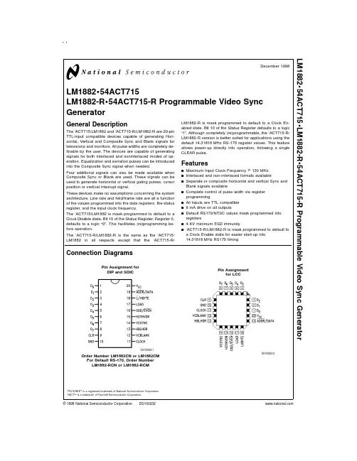
LM1882•54ACT715LM1882-R •54ACT715-R Programmable Video Sync GeneratorGeneral DescriptionThe ’ACT715/LM1882and ’ACT715-R/LM1882-R are 20-pin TTL-input compatible devices capable of generating Hori-zontal,Vertical and Composite Sync and Blank signals for televisions and monitors.All pulse widths are completely de-finable by the user.The devices are capable of generating signals for both interlaced and noninterlaced modes of op-eration.Equalization and serration pulses can be introduced into the Composite Sync signal when needed.Four additional signals can also be made available when Composite Sync or Blank are used.These signals can be used to generate horizontal or vertical gating pulses,cursor position or vertical Interrupt signal.These devices make no assumptions concerning the system architecture.Line rate and field/frame rate are all a function of the values programmed into the data registers,the status register,and the input clock frequency.The ’ACT715/LM1882is mask programmed to default to a Clock Disable state.Bit 10of the Status Register,Register 0,defaults to a logic “0”.This facilitates (re)programming be-fore operation.The ’ACT715-R/LM1882-R is the same as the ’ACT715/LM1882in all respects except that the ’ACT715-R/LM1882-R is mask programmed to default to a Clock En-abled state.Bit 10of the Status Register defaults to a logic “1”.Although completely (re)programmable,the ’ACT715-R/LM1882-R version is better suited for applications using the default 14.31818MHz RS-170register values.This feature allows power-up directly into operation,following a single CLEAR pulse.Featuresn Maximum Input Clock Frequency >130MHz n Interlaced and non-interlaced formats availablen Separate or composite horizontal and vertical Sync and Blank signals availablen Complete control of pulse width via register programmingn All inputs are TTL compatible n 8mA drive on all outputsn Default RS170/NTSC values mask programmed into registersn 4KV minimum ESD immunityn ’ACT715-R/LM1882-R is mask programmed to default to a Clock Enable state for easier start-up into 14.31818MHz RS170timingConnection DiagramsTRI-STATE ®is a registered trademark of National Semiconductor Corporation.FACT ™is a trademark of Fairchild Semiconductor Corporation.Pin Assignment for DIP and SOICDS100232-1Order Number LM1882CN or LM1882CM For Default RS-170,Order Number LM1882-RCN or LM1882-RCMPin Assignmentfor LCCDS100232-2December 1998LM1882•54ACT715•LM1882-R •54ACT715-R Programmable Video Sync Generator©1998National Semiconductor Corporation Logic Block Diagram Pin DescriptionThere are a Total of13inputs and5outputs on the’ACT715/ LM1882.Data Inputs D0–D7:The Data Input pins connect to the Ad-dress Register and the Data Input Register.ADDR/DATA:The ADDR/DATA signal is latched into the de-vice on the falling edge of the LOAD signal.The signal deter-mines if an address(0)or data(1)is present on the data bus. L/HBYTE:The L/HBYTE signal is latched into the device on the falling edge of the LOAD signal.The signal determines if data will be read into the8LSB’s(0)or the4MSB’s(1)of the Data Registers.A1on this pin when an ADDR/DATA is a0 enables Auto-Load Mode.LOAD:The LOAD control pin loads data into the Address or Data Registers on the rising edge.ADDR/DATA and L/HBYTE data is loaded into the device on the falling edge of the LOAD.The LOAD pin has been implemented as a Schmitt trigger input for better noise immunity.CLOCK:System CLOCK input from which all timing is de-rived.The clock pin has been implemented as a Schmitt trig-ger for better noise immunity.The CLOCK and the LOAD signal are asynchronous and independent.Output state changes occur on the falling edge of CLOCK.CLR:The CLEAR pin is an asynchronous input that initial-izes the device when it is HIGH.Initialization consists of set-ting all registers to their mask programmed values,and ini-tializing all counters,comparators and registers.The CLEAR pin has been implemented as a Schmitt trigger for better noise immunity.A CLEAR pulse should be asserted by the user immediately after power-up to ensure proper initializa-tion of the registers—even if the user plans to(re)program the device.Note:A CLEAR pulse will disable the CLOCK on the’ACT715/LM1882and will enable the CLOCK on the’ACT715-R/LM1882-R.ODD/EVEN:Output that identifies if display is in odd(HIGH) or even(LOW)field of interlace when device is in interlaced mode of operation.In noninterlaced mode of operation this output is always HIGH.Data can be serially scanned out on this pin during Scan Mode.VCSYNC:Outputs Vertical or Composite Sync signal based on value of the Status Register.Equalization and Serration pulses will(if enabled)be output on the VCSYNC signal in composite mode only.VCBLANK:Outputs Vertical or Composite Blanking signal based on value of the Status Register.HBLHDR:Outputs Horizontal Blanking signal,Horizontal Gating signal or Cursor Position based on value of the Sta-tus Register.HSYNVDR:Outputs Horizontal Sync signal,Vertical Gating signal or Vertical Interrupt signal based on value of Status Register.Register DescriptionAll of the data registers are12bits wide.Width’s of all pulses are defined by specifying the start count and end count of all pulses.Horizontal pulses are specified with-respect-to the number of clock pulses per line and vertical pulses are speci-fied with-respect-to the number of lines per frame.REG0—STATUS REGISTERThe Status Register controls the mode of operation,the sig-nals that are output and the polarity of these outputs.The de-fault value for the Status Register is0(000Hex)for the ’ACT715/LM1882and is“1024”(400Hex)for the ’ACT715-R/LM1882-R.DS100232-32Register Description(Continued)Bits0–2B2B1B0VCBLANK VCSYNC HBLHDR HSYNVDR 000CBLANK CSYNC HGATE VGATE (DEFAULT)001VBLANK CSYNC HBLANK VGATE 010CBLANK VSYNC HGATE HSYNC 011VBLANK VSYNC HBLANK HSYNC 100CBLANK CSYNC CURSOR VINT 101VBLANK CSYNC HBLANK VINT 110CBLANK VSYNC CURSOR HSYNC 111VBLANK VSYNC HBLANK HSYNCBits3–4B4B3Mode of Operation00Interlaced Double Serration and (DEFAULT)Equalization01Non Interlaced Double Serration10Illegal State11Non Interlaced Single Serration andEqualizationDouble Equalization and Serration mode will output equal-ization and serration pulses at twice the HSYNC frequency (i.e.,2equalization or serration pulses for every HSYNC pulse).Single Equalization and Serration mode will output an equalization or serration pulse for every HSYNC pulse.In Interlaced mode equalization and serration pulses will be output during the VBLANK period of every odd and even field.Interlaced Single Equalization and Serration mode is not possible with this part.Bits5–8Bits5through8control the polarity of the outputs.A value of zero in these bit locations indicates an output pulse active LOW.A value of1indicates an active HIGH pulse.B5—VCBLANK PolarityB6—VCSYNC PolarityB7—HBLHDR PolarityB8—HSYNVDR PolarityBits9–11Bits9through11enable several different features of the de-vice.B9—Enable Equalization/Serration Pulses(0)Disable Equalization/Serration Pulses(1)B10—Disable System Clock(0)Enable System Clock(1)Default values for B10are“0”in the’ACT715/LM1882and“1”in the’ACT715-R/LM1882-R.B11—Disable Counter Test Mode(0)Enable Counter Test Mode(1)This bit is not intended for the user but is for internaltesting only.HORIZONTAL INTERVAL REGISTERSThe Horizontal Interval Registers determine the number ofclock cycles per line and the characteristics of the HorizontalSync and Blank pulses.REG1—Horizontal Front PorchREG2—Horizontal Sync Pulse End TimeREG3—Horizontal Blanking WidthREG4—Horizontal Interval Width#of Clocks perLineVERTICAL INTERVAL REGISTERSThe Vertical Interval Registers determine the number of linesper frame,and the characteristics of the Vertical Blank andSync Pulses.REG5—Vertical Front PorchREG6—Vertical Sync Pulse End TimeREG7—Vertical Blanking WidthREG8—Vertical Interval Width#of Lines per FrameEQUALIZATION AND SERRATION PULSESPECIFICATION REGISTERSThese registers determine the width of equalization and ser-ration pulses and the vertical interval over which they occur.REG9—Equalization Pulse Width End TimeREG10—Serration Pulse Width End TimeREG11—Equalization/Serration Pulse VerticalInterval Start TimeREG12—Equalization/Serration Pulse VerticalInterval End TimeVERTICAL INTERRUPT SPECIFICATION REGISTERSThese Registers determine the width of the Vertical Interruptsignal if used.REG13—Vertical Interrupt Activate TimeREG14—Vertical Interrupt Deactivate TimeCURSOR LOCATION REGISTERSThese4registers determine the cursor position location,orthey generate separate Horizontal and Vertical Gating sig-nals.REG15—Horizontal Cursor Position Start TimeREG16—Horizontal Cursor Position End TimeREG17—Vertical Cursor Position Start TimeREG18—Vertical Cursor Position End TimeSignal SpecificationHORIZONTAL SYNC AND BLANKSPECIFICATIONSAll horizontal signals are defined by a start and end time.The start and end times are specified in number of clockcycles per line.The start of the horizontal line is consideredpulse1not0.All values of the horizontal timing registers arereferenced to the falling edge of the Horizontal Blank signal(see Figure1).Since the first CLOCK edge,CLOCK#1,causes the first falling edge of the Horizontal Blank referencepulse,edges referenced to this first Horizontal edge are n+1CLOCKs away,where“n”is the width of the timing in ques-tion.Registers1,2,and3are programmed in this manner.The horizontal counters start at1and count until HMAX.Thevalue of HMAX must be divisible by2.This limitation is im- 3Signal Specification(Continued)posed because during interlace operation this value is inter-nally divided by2in order to generate serration and equal-ization pulses at2x the horizontal frequency.Horizontal signals will change on the falling edge of the CLOCK signal. Signal specifications are shown below.Horizontal Period(HPER)=REG(4)x ckper Horizontal Blanking Width:=[REG(3)−1]x ckper Horizontal Sync Width:=[REG(2)−REG(1)]x ckper Horizontal Front Porch:=[REG(1)−1]x ckperVERTICAL SYNC AND BLANK SPECIFICATIONAll vertical signals are defined in terms of number of lines per frame.This is true in both interlaced and noninterlaced modes of operation.Care must be taken to not specify the Vertical Registers in terms of lines per field.Since the first CLOCK edge,CLOCK#1,causes the first falling edge of the Vertical Blank(first Horizontal Blank)reference pulse,edges referenced to this first edge are n+1lines away,where“n”is the width of the timing in question.Registers5,6,and7 are programmed in this manner.Also,in the interlaced mode,vertical timing is based on half-lines.Therefore regis-ters5,6,and7must contain a value twice the total horizontal (odd and even)plus1(as described above).In non-interlaced mode,all vertical timing is based on whole-lines.Register8is always based on whole-lines and does not add1for the first clock.The vertical counter starts at the value of1and counts until the value of VMAX.No re-strictions exist on the values placed in the vertical registers. Vertical Blank will change on the leading edge of HBLANK. Vertical Sync will change on the leading edge of HSYNC. (See Figure2.)Vertical Frame Period(VPER)=REG(8)x hperVertical Field Period(VPER/n)=REG(8)x hper/nVertical Blanking Width=[REG(7)−1]x hper/n Vertical Syncing Width=[REG(6)−REG(5)]x hper/n Vertical Front Porch=[REG(5)−1]x hper/nwhere n=1for noninterlacedn=2for interlacedCOMPOSITE SYNC AND BLANK SPECIFICATION Composite Sync and Blank signals are created by logically ANDing(ORing)the active LOW(HIGH)signals of the corre-sponding vertical and horizontal components of these sig-nals.The Composite Sync signal may also include serration and/or equalization pulses.The Serration pulse interval oc-curs in place of the Vertical Sync interval.Equalization pulses occur preceding and/or following the Serration pulses.The width and location of these pulses can be pro-grammed through the registers shown below.(See Figure3.) Horizontal Equalization PW=[REG(9)−REG(1)]x ckperREG9=(HFP)+(HEQP)+1 Horizontal Serration PW:=[REG(4)/n+REG(1)−REG(10)]x ckperREG10=(HFP)+(HPER/2)−(HSERR)+1 Where n=1for noninterlaced single serration/ equalizationn=2for noninterlaced double serration/equalizationn=2for interlaced operationDS100232-4FIGURE1.Horizontal Waveform Specification 4Signal Specification(Continued)HORIZONTAL AND VERTICAL GATING SIGNALSHorizontal Drive and Vertical Drive outputs can be utilized as general purpose Gating Signals.Horizontal and Vertical Gat-ing Signals are available for use when Composite Sync and Blank signals are selected and the value of Bit 2of the Sta-tus Register is 0.The Vertical Gating signal will change in the same manner as that specified for the Vertical Blank.Horizontal Gating Signal Width =[REG(16)−REG(15)]xckper Vertical Gating Signal Width:=[REG(18)−REG(17)]x hper CURSOR POSITION AND VERTICAL INTERRUPTThe Cursor Position and Vertical Interrupt signal are avail-able when Composite Sync and Blank signals are selected and Bit 2of the Status Register is set to the value of 1.The Cursor Position generates a single pulse of n clocks wide during every line that the cursor is specified.The signals are generated by logically ORing (ANDing)the active LOW (HIGH)signals specified by the registers used for generating Horizontal and Vertical Gating signals.The Vertical Interrupt signal generates a pulse during the vertical interval speci-fied.The Vertical Interrupt signal will change in the same manner as that specified for the Vertical Blanking signal.Horizontal Cursor Width =[REG(16)−REG(15)]x ckper Vertical Cursor Width =[REG(18)−REG(17)]x hper Vertical Interrupt Width =[REG(14)−REG(13)]x hperAddressing LogicThe register addressing logic is composed of two blocks of logic.The first is the address register and counter (AD-DRCNTR),and the second is the address decode (AD-DRDEC).ADDRCNTR LOGICAddresses for the data registers can be generated by one of two methods.Manual addressing requires that each byte of each register that needs to be loaded needs to be ad-dressed.To load both bytes of all 19registers would require a total of 57load cycles (19address and 38data cycles).Auto Addressing requires that only the initial register value be specified.The Auto Load sequence would require only 39load cycles to completely program all registers (1address and 38data cycles).In the auto load sequence the low order byte of the data register will be written first followed by the high order byte on the next load cycle.At the time the High Byte is written the address counter is incremented by 1.The counter has been implemented to loop on the initial value loaded into the address register.For example:If a value of 0was written into the address register then the counter would count from 0to 18before resetting back to 0.If a value of 15was written into the address register then the counter would count from 15to 18before looping back to 15.If a value greater than or equal to 18is placed into the address register the counter will continuously loop on this value.Auto ad-dressing is initiated on the falling edge of LOAD when AD-DRDATA is 0and LHBYTE is 1.Incrementing and loading of data registers will not commence until the falling edge of LOAD after ADDRDATA goes to 1.The next rising edge ofDS100232-5FIGURE 2.Vertical Waveform SpecificationDS100232-12FIGURE 3.Equalization/Serration Interval Programming5Addressing Logic(Continued)LOAD will load the first byte of data.Auto Incrementing is disabled on the falling edge of LOAD after ADDRDATA and LHBYTE goes low.Manual Addressing ModeCycle #Load Falling EdgeLoad Rising Edge 1Enable Manual Addressing Load Address m 2Enable Lbyte Data Load Load Lbyte m 3Enable Hbyte Data Load Load Hbyte m 4Enable Manual Addressing Load Address n 5Enable Lbyte Data Load Load Lbyte n 6Enable Hbyte Data LoadLoad Hbyte nAuto Addressing ModeCycle #Load Falling EdgeLoad Rising Edge1Enable Auto Addressing Load Start Address n 2Enable Lbyte Data Load Load Lbyte (n)3Enable Hbyte Data Load Load Hbyte (n);Inc Counter 4Enable Lbyte Data Load Load Lbyte (n+1)5Enable Hbyte Data Load Load Hbyte (n+1);Inc Counter 6Enable Manual AddressingLoad AddressADDRDEC LOGICThe ADDRDEC logic decodes the current address and gen-erates the enable signal for the appropriate register.The en-able values for the registers and counters change on the fall-ing edge of LOAD.Two types of ADDRDEC logic is enabled by 2pair of addresses,Addresses 22or 54(Vectored Re-start logic)and Addresses 23or 55(Vectored Clear logic).Loading these addresses will enable the appropriate logic and put the part into either a Restart (all counter registers are reinitialized with preprogrammed data)or Clear (all registers are cleared to zero)state.Reloading the same ADDRDEC address will not cause any change in the state of the part.The outputs during these states are frozen and the internalCLOCK is disabled.Clocking the part during a Vectored Re-start or Vectored Clear state will have no effect on the part.To resume operation in the new state,or disable the Vec-tored Restart or Vectored Clear state,another non-ADDRDEC address must be loaded.Operation will be-gin in the new state on the rising edge of the non-ADDRDEC load pulse.It is recommended that an unused address be loaded following an ADDRDEC operation to prevent data registers from accidentally being corrupted.The following Addresses are used by the device.Address 0Status Register REG0Address 1–18Data Registers REG1–REG18DS100232-7DS100232-86Addressing Logic(Continued)Address19–21UnusedAddress22/54Restart Vector(Restarts Device)Address23/55Clear Vector(Zeros All Registers)Address24–31UnusedAddress32–50Register Scan AddressesAddress51–53Counter Scan AddressesAddress56–63UnusedAt any given time only one register at most is selected.It is possible to have no registers selected.VECTORED RESTART ADDRESSThe function of addresses22(16H)or54(36H)are similar to that of the CLR pin except that the preprogramming of the registers is not affected.It is recommended but not required that this address is read after the initial device configuration load sequence.A1on the ADDRDATA pin(Auto Addressing Mode)will not cause this address to automatically incre-ment.The address will loop back onto itself regardless of the state of ADDRDATA unless the address on the Data inputs has been changed with ADDRDATA at0.VECTORED CLEAR ADDRESSAddresses23(17H)or55(37H)is used to clear all registers to zero simultaneously.This function may be desirable to use prior to loading new data into the Data or Status Registers. This address is read into the device in a similar fashion as all of the other registers.A1on the ADDRDATA pin(Auto Ad-dressing Mode)will not cause this address to automatically increment.The address will loop back onto itself regardless of the state of ADDRDATA unless the address on the Data inputs has been changed with ADDRDATA at0.GEN LOCKINGThe’ACT715/LM1882and’ACT715-R/LM1882-R is de-signed for master SYNC and BLANK signal generation. However,the devices can be synchronized(slaved)to an ex-ternal timing signal in a limited ing Vectored Re-start,the user can reset the counting sequence to a given lo-cation,the beginning,at a given time,the rising edge of the LOAD that removes Vector Restart.At this time the next CLOCK pulse will be CLOCK1and the count will restart at the beginning of the first odd line.Preconditioning the part during normal operation,before the desired synchronizing pulse,is necesasry.However,since LOAD and CLOCK are asynchronous and independent,this is possible without interruption or data and performance cor-ruption.If the defaulted14.31818MHz RS-170values are being used,preconditioning and restarting can be minimized by using the CLEAR pulse instead of the Vectored Restart operation.The’ACT715-R/LM1882-R is better suited for this application because it eliminates the need to program a1 into Bit10of the Status Register to enable the CLOCK.Gen Locking to another count location other than the very begin-ning or separate horizontal/vertical resetting is not possible with the’ACT715/LM1882nor the’ACT715-R/LM1882-R. SCAN MODE LOGICA scan mode is available in the ACT715/LM1882that allows the user to non-destructively verify the contents of the regis-ters.Scan mode is invoked through reading a scan address into the address register.The scan address of a given regis-ter is defined by the Data register address+32.The internal Clocking signal is disabled when a scan address is read. Disabling the clock freezes the device in it’s present state. Data can then be serially scanned out of the data registers through the ODD/EVEN Pin.The LSB will be scanned out first.Since each register is12bits wide,completely scanning out data of the addressed register will require12CLOCK pulses.More than12CLOCK pulses on the same register will only cause the MSB to repeat on the output. Re-scanning the same register will require that register to be reloaded.The value of the two horizontal counters and1ver-tical counter can also be scanned out by using address num-bers51–53.Note that before the part will scan out the data, the LOAD signal must be brought back HIGH.Normal device operation can be resumed by loading in a non-scan address.As the scanning of the registers is a non-destructive scan,the device will resume correct opera-tion from the point at which it was halted.RS170Default Register ValuesThe tables below show the values programmed for the RS170Format(using a14.31818MHz clock signal)and how they compare against the actual EIA RS170Specifica-tions.The default signals that will be output are CSYNC, CBLANK,HDRIVE and VDRIVE.The device initially starts at the beginning of the odd field of interlace.All signals have active low pulses and the clock is disabled at power up.Reg-isters13and14are not involved in the actual signal informa-tion.If the Vertical Interrupt was selected so that a pulse in-dicating the active lines would be output.DS100232-9FIGURE4.ADDRDEC Timing7RS170Default Register Values(Continued)Reg D Value H Register DescriptionREG00000Status Register(715/LM1882)REG01024400Status Register(715-R/LM1882-R)REG123017HFP End TimeREG29105B HSYNC Pulse End TimeREG315709D HBLANK Pulse End TimeREG491038E Total Horizontal ClocksREG57007VFP End TimeREG61300D VSYNC Pulse End TimeREG741029VBLANK Pulse End TimeREG852520D Total Vertical LinesREG957039Equalization Pulse End TimeREG1041019A Serration Pulse Start TimeREG111001Pulse Interval Start TimeREG1219013Pulse Interval End TimeREG1341029Vertical Interrupt Activate TimeREG1452620E Vertical Interrupt Deactivate TimeREG1591138F Horizontal Drive Start TimeREG169205C Horizontal Drive End TimeREG171001Vertical Drive Start TimeREG1821015Vertical Drive End TimeRate PeriodInput Clock14.31818MHz69.841nsLine Rate15.73426kHz63.556µsField Rate59.94Hz16.683msFrame Rate29.97Hz33.367msRS170Horizontal DataSignal Widthµs%H Specification(µs)HFP22Clocks 1.536 1.5±0.1 HSYNC Width68Clocks 4.7497.47 4.7±0.1 HBLANK Width156Clocks10.89517.1510.9±0.2 HDRIVE Width91Clocks 6.35610.000.1H±0.005H HEQP Width34Clocks 2.375 3.74 2.3±0.1 HSERR Width68Clocks 4.7497.47 4.7±0.1HPER iod910Clocks63.556100RS170Vertical DataVFP3Lines190.676EQP Pulses VSYNC Width3Lines190.676Serration Pulses VBLANK Width20Lines1271.127.620.075V±0.005V VDRIVE Width11.0Lines699.12 4.200.04V±0.006V VEQP Intrvl9Lines 3.639Lines/Field VPERiod(field)262.5Lines16.683ms16.683ms/Field VPERiod(frame)525Lines33.367ms33.367ms/Frame8Absolute Maximum Ratings(Note1)If Military/Aerospace specified devices are required, please contact the National Semiconductor Sales Office/ Distributors for availability and specifications.Supply Voltage(V CC)−0.5V to+7.0V DC Input Diode Current(I IK)V I=−0.5V−20mA V I=V CC+0.5V+20mA DC Input Voltage(V I)−0.5V to V CC+0.5V DC Output Diode Current(I OK)V O=−0.5V−20mA V O=V CC+0.5V+20mA DC Output Voltage(V O)−0.5V to V CC+0.5V DC Output Sourceor Sink Current(I O)±15mA DC V CC or Ground Currentper Output Pin(I CC or I GND)±20mA Storage Temperature(T STG)−65˚C to+150˚C Junction Temperature(T J)Ceramic175˚C Plastic140˚CRecommended Operating ConditionsSupply Voltage(V CC) 4.5V to5.5V Input Voltage(V I)0V to V CC Output Voltage(V O)0V to V CC Operating Temperature(T A)54ACT−55˚C to+125˚C Minimum Input Edge Rate(∆V/∆t)V IN from0.8V to2.0VV CC@4.5V,5.5V125mV/ns Note1:Absolute maximum ratings are those values beyond which damage to the device may occur.The databook specifications should be met,without exception,to ensure that the system design is reliable over its power supply, temperature and output/input loading variables.National does not recom-mend operation of FACT®circuits outside databook specifications.DC CharacteristicsFor’ACT Family Devices over Operating Temperature Range(unless otherwise specified)LM188254ACT/LM1882LM1882V CC T A=+25˚C T A=−55˚C T A=−40˚CSymbol Parameter(V)C L=50pF to+125˚C to+85˚C Units ConditionsC L=50pFTyp Guaranteed LimitsV OH Minimum High Level 4.5 4.49 4.4 4.4 4.4V I OUT=−50µA Output Voltage 5.5 5.49 5.4 5.4 5.4V(Note2)4.5 3.86 3.7 3.76V V IN=V IL/V IH5.5 4.86 4.7 4.76V I OH=−8mAV OL Maximum Low Level 4.50.0010.10.10.1V I OUT=50µA Output Voltage 5.50.0010.10.10.1V(Note2)4.50.360.50.44V V IN=V IL/V IH5.50.360.50.44V I OH=+8mAI OLD Minimum Dynamic 5.532.032.0mA V OLD=1.65VOutput CurrentI OHD Minimum Dynamic 5.5−32.0−32.0mA V OHD=3.85VOutput CurrentI IN Maximum Input 5.5±0.1±1.0±1.0µA V I=V CC,GNDLeakage CurrentI CC Supply Current 5.58.016080µA V IN=V CC,GNDQuiescentI CCT Maximum I CC/Input 5.50.6 1.6 1.5mA V IN=V CC−2.1VNote2:All outputs loaded;thresholds on input associated with input under test.Note3:Test Load50pF,500Ωto Ground.9AC Electrical CharacteristicsLM188254ACT/LM1882LM1882V CC T A=+25˚C T A=−55˚C T A=−40˚CSymbol Parameter(V)C L=50pF to+125˚C to+85˚C UnitsC L=50pF C L=50pFMin Typ Max Min Max Min Maxf MAXI Interlaced f MAX 5.0170190130150MHz(HMAX/2is ODD)f MAX Non-Interlaced f MAX 5.0190220145175MHz(HMAX/2is EVEN)t PLH1Clock to Any Output 5.0 4.013.015.5 3.519.5 3.518.5ns t PHL1t PLH2Clock to ODDEVEN 5.0 4.515.017.0 3.522.0 3.520.5ns t PHL2(Scan Mode)t PLH3Load to Outputs 5.0 4.011.516.0 3.020.0 3.019.5nsAC Operating RequirementsLM188254ACT/LM1882LM1882 Symbol Parameter V CC T A=+25˚C T A=−55˚C T A=−40˚C Units(V)to+125˚C to+85˚CTyp Guaranteed MinimumsControl Setup Timet sc ADDR/DATA to LOAD− 5.0 3.0 4.0 4.5 4.5nst sc L/HBYTE to LOAD− 3.0 4.0 4.5 4.5ns Data Setup Timet sd D7–D0to LOAD+ 5.0 2.0 4.0 4.5 4.5ns Control Hold Timet hc LOAD−to ADDR/DATA 5.00 1.0 1.0 1.0ns LOAD−to L/HBYTE0 1.0 1.0 1.0nsData Hold Timet hd LOAD+to D7–D0 5.0 1.0 2.0 2.0 2.0nst rec LOAD+to CLK(Note4) 5.0 5.57.08.08.0ns Load Pulse Widtht wld−LOW 5.0 3.0 5.5 5.5 5.5nst wld+HIGH 5.0 3.0 5.07.57.5nst wclr CLR Pulse Width HIGH 5.0 5.5 6.59.59.5nst wck CLOCK Pulse Width 5.0 2.5 3.0 4.0 3.5ns (HIGH or LOW)Note4:Removal of Vectored Reset or Restart to Clock.CapacitanceSymbol Parameter Typ Units ConditionsC IN Input Capacitance7.0pF V CC=5.0VC PD Power Dissipation17.0pF V CC=5.0VCapacitance10。