纳米压痕实验培训资料.ppt
- 格式:ppt
- 大小:2.88 MB
- 文档页数:14
纳米压痕技术实验及其应用简介纳米压痕技术(Nanoindentation)是一种用于研究材料力学性质的精密技术。
通过在材料表面施加一定载荷,然后测量载荷与压痕深度之间的关系,可以得到材料的硬度、弹性模量等力学性质。
本文将介绍纳米压痕技术的基本原理、实验步骤以及在材料科学领域中的应用。
基本原理纳米压痕技术基本原理是利用钢球或金刚石尖端通过纳米压头在被测材料表面施加载荷,然后测量载荷与压痕深度的关系。
通过分析载荷-压痕深度曲线,可以获得材料的硬度、弹性模量等力学参数。
实验步骤1.样品制备:制备需要进行纳米压痕实验的材料样品,通常是块状的金属、陶瓷、聚合物等材料。
2.仪器校准:校准纳米压头的载荷传感器和位移传感器,确保实验数据准确可靠。
3.压痕实验:在样品表面选取合适的位置进行压痕实验,在一定载荷范围内施加载荷并记录载荷-压痕深度曲线。
4.数据处理:通过数据处理软件对实验数据进行分析,计算得到材料的硬度、弹性模量等力学参数。
应用领域纳米压痕技术在材料科学领域中有着广泛的应用,主要包括:•材料硬度测试:纳米压痕技术可以准确测量材料的硬度,对于评估材料的力学性能非常重要。
•薄膜力学性质研究:对于薄膜材料而言,纳米压痕技术可以有效地评估其力学性质。
•生物材料力学性质研究:在生物材料研究领域,纳米压痕技术可以帮助科研人员了解生物材料的力学性能,如骨骼、牙齿等。
结论纳米压痕技术作为一种精密的材料力学测试方法,在材料科学领域有着广泛的应用前景。
通过实验分析,可以更准确地评估材料的力学性能,为材料设计和研发提供重要参考。
以上就是关于纳米压痕技术实验及其应用的文档内容,希术能对您有所帮助。


纳米压痕实验报告(一)引言概述:纳米压痕实验是一种常用的材料力学测试方法,通过对材料进行微小压痕,可以研究材料的力学性能和变形行为。
本文将对纳米压痕实验的方法、实验装置、实验步骤、测试参数和结果进行详细介绍和分析,以期为深入了解纳米压痕实验提供参考。
正文:一、纳米压痕实验方法1.1 传统压痕法与纳米压痕法的区别1.2 纳米压痕实验的优势与应用场景1.3 实验材料的选择与准备二、纳米压痕实验装置2.1 纳米压痕仪器的组成与工作原理2.2 纳米压头的结构与功能2.3 实验中所需的辅助设备及其作用三、纳米压痕实验步骤3.1 样品的加工与制备3.2 实验前的样品表面处理3.3 压痕参数的设置与调整3.4 压痕实验的操作步骤3.5 实验后样品的处理与测量四、纳米压痕实验参数与理论分析4.1 压痕深度与硬度的关系分析4.2 压痕直径与弹性模量的计算方法4.3 弹性回弹与塑性变形的测定4.4 扩展失效与压痕形变的研究4.5 温度对压痕行为的影响五、纳米压痕实验结果与讨论5.1 实验样品的压痕图像与参数5.2 不同材料的压痕行为对比5.3 纳米压痕实验的数据可靠性与重复性5.4 工程应用中的纳米压痕实验案例5.5 纳米压痕实验的未来发展趋势总结:通过本次纳米压痕实验,我们深入了解了纳米压痕实验的方法、实验装置、实验步骤、测试参数和结果。
纳米压痕实验在材料力学研究和工程应用中具有重要的价值,通过对材料的微小压痕分析,可以获得材料的力学性能、变形行为等关键信息。
随着纳米技术的不断发展,纳米压痕实验将在材料科学、纳米材料、生物材料等领域的应用得到更广泛的拓展和深入研究。


利用纳米压痕技术研究材料力学性能的实验方法和数据处理纳米压痕技术是一种用于研究材料力学性能的重要实验方法,它可以通过在纳米尺度下对材料进行压痕测试,得到材料的硬度、弹性模量等力学性能参数。
本文将介绍纳米压痕技术的实验方法,并讨论如何进行数据处理和分析。
一、纳米压痕实验方法纳米压痕实验通常采用纳米硬度计进行。
纳米硬度计具有一个具有知名几何形状的金刚石扣、压头、压头和试样间的距离控制装置类似恒定速率模式(法的独特设计和控制技术。
实验步骤如下:1.样品制备:将所要测试的材料制备成平整的样品。
通常可以使用机械研磨、电子抛光等方法对样品进行制备和表面处理。
2.样品安装:在纳米硬度计的测试平台上安装样品。
确保样品表面垂直于压头的运动方向,以获得准确的测试结果。
3.压痕力的选择:根据所要研究的材料的硬度,选择合适的压痕力。
通常,压痕力在几微牛到几百微牛之间。
4.压痕测试:将压头缓慢逼近试样表面,直到产生明显的弹性变形。
然后继续加大压痕力,直到达到设定的最大力值。
此过程中,纳米硬度计会实时记录压头的位置和力值。
5.压头退休:当压痕测试结束后,压头会逐渐从试样表面移开,直到与试样分离为止。
6.数据记录:在测试过程中,纳米硬度计会实时记录测试数据,包括压头的位置和力值。
这些数据可以用于后续的数据处理和分析。
二、数据处理和分析1.压头形状校正:由于压头的几何形状可能会对测试结果产生影响,因此需要对测试数据进行压头形状校正。
常见的方法是通过使用已知硬度和弹性模量的标准材料进行校正计算。
2.压痕深度测量:根据压头的位置和试样的厚度,可以计算出压痕的深度。
压痕深度与试样的硬度和弹性模量相关联,可以用于后续的力学性能参数计算和分析。
3.力位曲线分析:力位曲线是指在测试过程中纳米硬度计记录的压头位置和力值的曲线。
通过分析力位曲线,可以获得材料的硬度、弹性模量、塑性变形等力学性能参数。
4. 转化计算:通过引入相关的力学模型和计算公式,可以将压痕测试得到的数据转化为所研究材料的力学性能参数。
纳米压痕原理纳米压痕技术是一种用于材料表面硬度和弹性模量测量的先进技术。
它是由威廉姆斯和奥利弗在1992年首次提出的,通过在纳米尺度下施加压痕来研究材料的力学性能。
纳米压痕技术已经被广泛应用于材料科学、纳米材料、薄膜材料、生物材料、金属材料等领域。
纳米压痕原理基于弹性理论和塑性变形理论,通过在纳米尺度下施加压痕来研究材料的硬度、弹性模量和塑性变形行为。
纳米压痕技术主要包括压头和样品的接触、加载、保持和卸载四个阶段。
在压头和样品接触阶段,压头逐渐接触到样品表面直到建立稳定的接触。
在加载阶段,压头施加载荷并逐渐形成压痕,记录载荷和压头位移的关系。
在保持阶段,保持载荷不变,使压头停留在最大载荷位置,记录载荷和时间的关系。
最后在卸载阶段,卸载载荷并记录载荷和压头位移的关系。
纳米压痕技术的原理是通过对压头载荷和位移的关系进行分析,可以得出样品的硬度和弹性模量等力学性能参数。
硬度是材料抵抗外界力量侵入的能力,是材料表面的一个重要力学性能参数;弹性模量是材料在弹性阶段的应力和应变关系,是材料的一个重要弹性参数。
通过纳米压痕技术可以实现对材料力学性能的定量分析和表征。
纳米压痕技术具有高分辨率、无损伤、样品制备简单、操作方便等优点,已经成为研究材料力学性能的重要手段。
它在材料科学、纳米材料、薄膜材料、生物材料、金属材料等领域有着广泛的应用前景。
通过对纳米压痕原理的深入理解和研究,可以推动材料力学性能表征技术的发展,为材料设计和制备提供重要的理论和实验基础。
总之,纳米压痕原理是一种重要的材料力学性能表征技术,通过对压头载荷和位移的关系进行分析,可以得出样品的硬度和弹性模量等力学性能参数。
纳米压痕技术具有高分辨率、无损伤、样品制备简单、操作方便等优点,已经成为研究材料力学性能的重要手段。
通过对纳米压痕原理的深入理解和研究,可以推动材料力学性能表征技术的发展,为材料设计和制备提供重要的理论和实验基础。

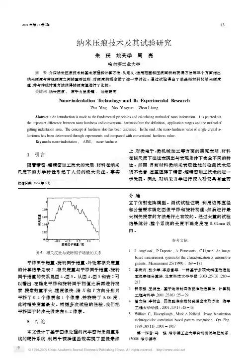
图5 相关度量与旋转因子增量的关系平移因子增量、旋转因子增量、外轮廓相关度量的计算结果见表2,相关度量与平移因子增量、旋转因子增量的关系见图4、图5。
从图4、图5和表2可以看出,在确定平移和旋转因子初值之后再进行搜索,搜索数量不大,速度很快;沿X和Y方向分别只平移了012个像素和1个像素,并旋转了0106度,此时相关度量最大。
根据多次试验的经验,我们把平移因子的步长设定在012像素。
5 结论本文设计了基于图像处理的汽车密封条测量系统的硬件系统,利用牛顿插值函数实现了亚像素细分,建立了仿射变换模型。
测试试验证明:利用边界直径和公差要求确定图像平移和旋转初值、然后进行最大相关搜索的方法是行之有效的。
经过大量的试验结果统计,整个系统的长度不确定度在0102mm以内。
参考文献1 L Angrisani,P Daponte,A Pietrosanto,C Liguori.An image based measurement system for the characterization of autom otive gaskets.Measurement25(1999):169~1812 李庆利,张少军,李忠富等.一种基于多项式插值改进地亚像素细分算法.北京科技大学学报,2003,25(3):280~2833 钟家强,王润生.基于边缘的图像配准改进算法.计算机工程与科学,2001,23(6):25~294 曾文峰,李树山.图像配准参数的自适应求取方法.海军工程大学学报,2001,13(1):45~485 William C,Hasenplaugh,Mark A Neifeld.Image binarization techniques for correlation based pattern recognition.Opt Eng.1999,38(11):1907~1917第一作者:马 强,哈尔滨工业大学自动测试与控制系, 150001哈尔滨市收稿日期:2004年3月纳米压痕技术及其试验研究朱 瑛 姚英学 周 亮哈尔滨工业大学摘 要:介绍纳米压痕技术的基本原理和计算方法,从定义、适用范围和压痕面积的获得方法等三个方面指出纳米硬度与常规硬度之间的重要区别,对硬度的概念做了进一步讨论。
纳米压痕技术(英:Nanoindentation),也称深度敏感压痕技术(英:Depth-Sensing Indentation, DSI),是最简单的测试材料力学性质的方法之一,可以在纳米尺度上测量材料的各种力学性质,如载荷-位移曲线、弹性模量(Elastic Modulus)、硬度(Hardness)、断裂韧性(Frac ture Toughness)、应变硬化效应(Strain Hardening Effect)、粘弹性使材料发生一定弹性变形的应力也越大,即材料刚度越大,亦即在一定应力作用下,发生弹性变形越小。
弹性模量E是指材料在外力作用下产生单位弹性变形所需要的应力。
它是反映材料抵抗弹性变形能力的指标,相当于普通弹簧中的刚度。
晶体管,本名是半导体三极管,是内部含有两个PN结,外部通常为三个引出电极的半导体器件。
它对电信号有放大和开关等作用,应用十分广泛。
能隙(Bandgap energy gap)或译作能带隙,在固态物理学中泛指半导体或是绝缘体的价带(valenc e band)(价带[1](valenc e band)或称价电带,通常是指半导体或绝缘体中,在绝对零度下能被电子占满的最高能带。
对半导体而言,此能带中的能级基本上是连续的。
全充满的能带中的电子不能在固体中自由运动。
但若该电子受它可吸收足够能量而跳入下一个容许的最高能区,从而使价带变成部分充带中留下的电子可在固体中自由运动。
)顶端至传导带(传导带(conduction band)系指半导体或是绝缘体材料中,一个电子所具有能量的范围。
这个能量的范围高于价带(valence band),而所有在传导带中的电子均可经由外在的电场加速而形成电流)(conduction band)底端的能量差距, 对一个本征半导体(intrinsic semic onduc tor)而言,其导电性与能隙的大小有关,只有获得足够能量的电子才能从价带被激发,跨过能隙并跃迁至传导带。
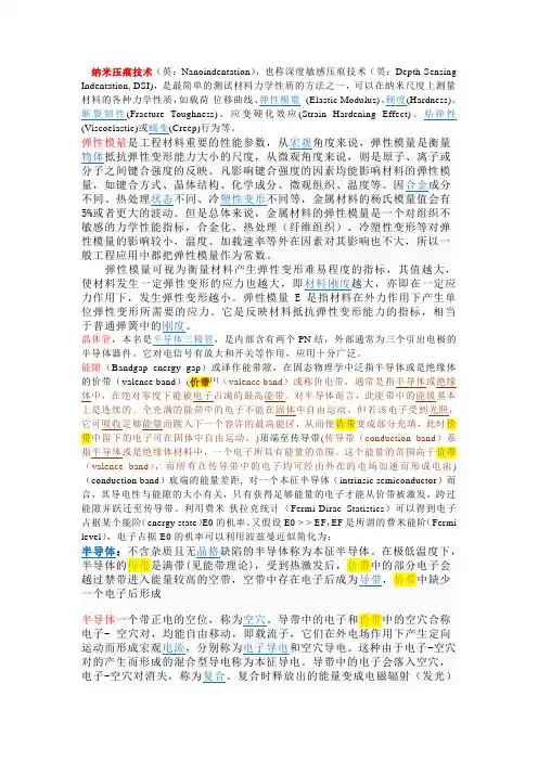
Measurements of mechanical properties and number of layers of graphene from nano-indentationYupeng Zhang a ,Chunxu Pan a ,b ,⁎a School of Physics and Technology and Key Laboratory of Arti ficial Micro-and Nano-structures of Ministry of Education,Wuhan University,Wuhan,430072,PR China bCenter for Electron Microscopy,Wuhan University,Wuhan 430072,PR Chinaa b s t r a c ta r t i c l e i n f o Article history:Received 13October 2011Received in revised form 12January 2012Accepted 25January 2012Available online 9February 2012Keywords:GrapheneNumber of layersMechanical properties NanoindentationIn this paper,we introduce an approach to simply and effectively determine the mechanical property and number of layers of graphene simultaneously from one indentation by using an instrumented nano-indenter.The results reveal that the elastic modulus of a single layer graphene is 0.89TPa after correction of the effect of substrate,which is coincident to the experimental and theoretical data from other researches.In addition,it is found that there exist a linear relationship between the number of layers and the hardness of graphene,which provide a novel and also effective method for judging the number of graphene layers.©2012Elsevier B.V.All rights reserved.1.IntroductionGraphene is a two-dimensional (2D)crystal which is made up of sp2–hybridized carbon atom.The recent researches have revealed that graphene possesses many remarkable properties,such as high thermal conductivity (5000Wm –1K –1),[1]high charge carrier mo-bility (15,000cm 2V –1s –1)at room temperature [2]and the calculat-ed value of speci fic surface area up to 2630m 2g –1,[3]which promise the wide potential applications in graphene-based composites [4],nano devices [5],energy storage materials [6]and so on.In general,less than 10layers of graphite are all de fined as gra-phene,different layers of graphene exhibit variant band structure,and the physical,chemical and mechanical properties of graphene are strongly related to the number of layers [7,8].Therefore,a simpler and more accurate method for characterizing the layer of graphene is crucial to determine its properties and further applications.So far,the layers of graphene can be accurately characterized by using approaches involving Raman spectrum or high-resolution transmis-sion electronic microscopy (HRTEM).In Raman spectrometry,the number of graphene layers is determined according to the G peak and D peak second order (2D peak)changing in shape,width,and position [9–11].When using the HRTEM observation,the number of graphene layers can be directly con firmed by counting lines at the graphene edge [12,13].In addition,the regular optical microscopehas also been used for revealing the thickness variation of graphene layers when the graphene is deposited upon the Si substrate with a 300nm SiO 2film,because of a strong amplitude modulation of re flec-tion at the air –graphene-SiO 2interface [14–16].Compared to evaluation for physical and chemical properties of graphene,the measurement of mechanical property including elastic modulus,breaking strength,bending stiffness,elastic deformation,failure,hardness and flexibility are much more dif ficult due to limita-tion of the present techniques.So far,the theoretical calculations for monolayer graphene have con firmed the elastic modulus from 0.8to 1.1TPa [17–19].Meanwhile the experimental test of graphene was performed by nano-indentation using an atom force microscope (AFM)tip upon a free-standing graphene sheets [20–24].The elastic modulus is calculated from a load –displacement curve,and the re-sults show that modulus could achieve 1.0±0.1TPa similarly [20,21].All of these researches demonstrated that graphene is the strongest material and may be a promising reinforcement of nano-composites [25,26].In recent years,the instrumented nano-indentation techniques have been widely used in the characterization of small scale mechan-ical behavior of materials [27–29].It can continuously measure the load and displacement as small as 1nN and 0.1nm respectively.From the load –displacement data,the mechanical properties includ-ing hardness and elastic modulus can be determined without imaging the indentation.In addition,compared with AFM,the instrumented nano-indentation adopts the continuous stiffness measurement (CSM)technique to collect a continuous data with thickness.CSM is accomplished by imposing a small,sinusoidal varying signal on top of a DC signal that drives the motion of the indenter.This allows the measurement of contact stiffness at any point along the loadingDiamond &Related Materials 24(2012)1–5⁎Corresponding author at:School of Physics and Technology and Key Laboratory of Arti ficial Micro-and Nano-structures of Ministry of Education,Wuhan University,Wuhan,430072,PR China.Tel.:+862768752481x5201.E-mail address:cxpan@ (C.Pan).0925-9635/$–see front matter ©2012Elsevier B.V.All rights reserved.doi:10.1016/j.diamond.2012.01.033Contents lists available at SciVerse ScienceDirectDiamond &Related Materialsj o u r n a l h om e p a g e :ww w.e l s e v i e r.c o m /l o c a t e /d i a m o n dcurve and obtains the hardness and elastic modulus at exceedingly small penetration depths.Thus,this technique provides an ideal ap-proach for measuring nano-films upon a substrate.Obviously,the graphene sheets should respond to the instrumen-ted nano-indentation due to its high strength and elastic modulus, which is not reported in any literature up to now.In this paper,we intend to simply obtain the information such as the number of graphene layers,hardness and elastic modulus from the response of graphene to the instrumented nano-indenter.2.Experimental detailsIn this work,graphene oxide(GO)was synthesized by a modified Hummers method[30,31]:the graphite powder(0.3g)was putintoFig.1.The micrograph of indentation location and the experiment results acquired from the instrumented nano-indenter.a,Optical microscope image of graphene on the Si sub-strate with a285nm thick SiO2film,graphene with different apparent colors was marked with A B C D and E.b,The experimental result of AFM,from which the change of graphene layers can be more clearly identified,there are1,2,3,4and above4layers respective.c,The hardness–displacement curves of different layers graphene,inset in c shows the hard-ness change in the range of20–50nm.d,The elastic modulus–displacement curves of different layers graphene,inset in d shows the modulus change in the range of20–50nm. e,The continuous stiffness measurement(CSM)of different layers graphene,inset in e shows the change of continuous stiffness in the range of0–30nm.f,The load–displacement curves of different layers graphene,inset in f shows the load change in the range of0–50nm.2Y.Zhang,C.Pan/Diamond&Related Materials24(2012)1–5the solution contained2–4mL concentrated H2SO4,0.5g K2S2O4and 0.5g P2O5.The resultant dark blue mixture was kept stirring for4h at 80°C,and then was carefully diluted with distilled water,the initial product was obtained byfiltering and drying at ambient temperature. Subsequently,the initial product was re-dispersed into12mL con-centrated H2SO4,and1.5g KMnO4was added laggardly.An ice bath should be used in order to avoid the temperature increasing over 20°C.The mixture was stirred at35°C for2h,and25mL distilled water was added.70mL distilled water and2mL30%H2O2solution were added and the reaction was terminated in15minutes.Then the color of the mixture was changed from snuff color to bright yel-low.At last,the mixture was washed by HCl solution and distilled water in turn until the PH value of rinse water became neutral,and the GO was obtained after drying.Ethanol suspensions of the GO were spin-coated the Si substratewith a300nm thick SiO2film.The GO sheets were charged into a quartz tube and purged with argon,and then reduced to graphene at1000°C in vacuum with the heating rate100°C/min.The graphene thickness was evaluated using an optical micro-scope(Olympus,cover–018,Japan)for determining the position of nanoindentation.The corresponding number of graphene layers was characterized using an AFM(Seiko,SPI4000PROBE STASTM,Japan).Nano-indentation experiments were carried out on an instrumen-ted nano-indenter(Agilent,nano indenter G200,USA)with the meth-od of continues stiffness measurement(CSM).A diamond Berkovich indenter with a tip radius R≈20nm was used.Experiment parame-ters are as follows:the constant value of Poisson ratio is0.17 [32,33],the vibration frequency of indenter is45Hz and the maxi-mum indentation depth is500nm.3.Results and discussionFig.1(a)shows an optical image of the graphene.According to the different color contrast,the thickness of graphene can be clearly identi-fied and marked as A,B,C,D and E.AFM experiment reveals the corre-sponding number of graphene layers at the area,as shown in Fig.1(b).Fig.1(c)and(d)illustrates the hardness–displacement and elastic modulus–displacement curves at different graphene layers by using the nano-indentation.It is found that a large dip appears in the range of depth less than10nm,and then the curves increase gradual-ly to a stable values.Further continuous stiffness measurement(CSM) indicates that there is an inflexion around the depth of10nm,as shown in Fig.1(e),which is correspond to the points of the peaks in Fig.1(c)and(d).In addition,the load–displacement curve clearly reveals that the load on the graphene decreases with the number of layers increasing at the same indentation depth,as shown in Fig.1(f).Similarly,the phenomenon also appears in Fig.1(c)and(d),in which the hardness and the elastic modulus of the graphene decrease with the increase of the layers.3.1.Measurement of the elastic modulus of grapheneIn the present graphene/SiO2system such as a hardfilm on a soft substrate,the hardness and elastic modulus decrease with an increasing of contact depth.Therefore,the peak in the hardness–displacement and elastic modulus–displacement curves,as shown in Fig.1(c)and (d),indicates the response of high hardness and modulus of graphene to the indenter.However,due to the very thin thickness of graphene, it is impossible to obtain the value of hardness and elastic modulus of pure graphene directly from the curves,the effect of soft SiO2film below graphene must be considered during indenting.Fig.2illustrates the variant of monolayer graphene sheet under different loads.When indenter contact graphene,the deformation of graphene start in the axial direction.And then,carbon network of graphene will be broken as indentation depth increasing.Therefore,hardness and modulus could be obtained through the load–displace-ment curve.However,the measured value of hardness and modulus involves two portions,SiO2substrate and graphene.For example,in the case of a monolayer graphene,when the indentation depth reaches to 8nm,the total energy of indenter acted upon the surface can be cal-culated from the load–displacement curve of monolayer graphene,as show in Fig.3(a).The value is from the following Eq.(1):W¼∫80:00207xþ2:13933EÀ4x2dx¼10:1E−14Jð1ÞFig.2.The deformation of monolayer graphene sheet under different loads.a,graphene sheet under no load.b,deformation under the pressure P.c,crack under the maximal pressure P m.Fig.3.a,Thefitting curve to the load–displacement curve of monolayer graphene, though which the total energy provided by indenter can be calculated.b,The variation-al trend of bond energy in the proportion of total energy as the indentation displace-ment increase.3Y.Zhang,C.Pan/Diamond&Related Materials24(2012)1–5At this time,the portion of the energy for breaking C–C bonds will be7.48E−14J,which is calculated based on the hypothesis:1)The indentation area is A c=24.5h c2,where the depth h c=8nm,and then A c=1568nm2;2)The C–C bond length is0.14nm,and the energy for breaking one C–C bond is650kJ/mol;3)The total energy to break C–C bonds in the area is equal to A c divided by one area of the carbon honeycomb network.Obviously,the total energy is larger than the energy to break pure graphene,and the rest value is from the SiO2film.The calculation according to Fig.3(a)and Eq.(1)roughly illustrates that the portion of energy to break the graphene bond decreases with the depth in-crease from2nm to200nm,and there is a rapid reduction before around10nm,as shown in Table1and Fig.3(b),which actually cor-responds to the peak forms in the hardness–displacement and elastic modulus–displacement curves,as shown in Fig.1(a)and(b).After the peaks,the curves increase gradually with increasing of the depth in the range of10–200nm andfinally reach a nearly con-stant value,which is the typical profile of a soft SiO2film on a hard Si substrate[34].The above discussion demonstrates that the value of elastic mod-ulus of graphene can be experimentally and simply obtained from the elastic modulus–displacement curve.Considering to the effect of sub-strate,the corrected value can be calculated from the following Eq.(2)[35]:1 r ¼1−v2iiþ1−v2ff1−e−αtþ1−v2sse−αt;ð2Þwhere E r is the reduced elastic modulus,E i,E f,E s are elastic modulus of the indenter,film(graphene)and SiO2substrate,respectively.v i, v f and v s are Poisson's ratio of the indenter,film and substrate,respec-tively.αis a constant related with the indenter geometry,according to King's method[36],selectingα=1.3.t is thefilm(graphene) thickness under the indenter and a is the square root of the projected contact area.The results show,for example,that for a monolayer graphene,the experimental value of elastic modulus is0.3TPa,and the modified value is0.89TPa,as listed in Table2,which is consistent with the value of1.0TPa reported in current literatures[17,18].Therefore, the present instrumented nano-indentation provides an effective and simple approach for measure mechanical properties of graphene.3.2.Measurement of the number of graphene layersFrom Fig.1(c),(d),(f)and the corresponding Table2,we can clearlyfind that the heights of the curves changed with the increase of number of graphene layers.The divergences between the graphene with different number of layers are listed in Table3.It is interested to note that there exists an approximate linear relationship according to the above data,as shown in Fig.4.Relatively,Fig.4(a)exhibits a bet-ter linear phenomenon from the hardness–displacement curve.This softening effect also was observed in Changgu Lee et al.'s work,an AFM probe tip indents upon a free-standing graphenefilm [18].They proposed a possible explanation for the phenomenon base on the slip between the graphene layers,and not from plastic de-formation.That is to say,when the tip indents the multilayer mem-brane,the slight bending in the membrane under the tip causes a difference of elongation between the layers.Slip will occur when the elongation difference between the layers is equal to the C–C bond length,which is about0.14nm.Table1The value of bond energy of graphene and the total energy provided by indenter.Depth(nm)2582050100200Bond energy(J) 4.68E−15 2.92E−147.48E−14 4.68E−13 2.92E−12 1.17E−11 4.68E−11 Total energy(J) 4.73E−15 3.45E−1410.1E−149.53E−1310.95E−127.72E−11 5.75E−10 %98.986.674.149.126.715.28.1Table2Hardness and elastic modulus of different layers graphene using nano indentation,themodified value of elastic modulus calculated exclude the substrate effect.Monolayer (A)Bilayer(B)Trilayer(C)Tetralayer(D)Multilayerabove4(E)Hardness (TPa)Exp.data0.950.270.230.190.10 Modified data–––––Modulus (TPa)Exp.data0.3050.1200.700.410.37 Modified data0.8910.3930.0510.0270.027Table3The average variation of elastic modulus and hardness between different layers gra-phene in the range of10–500nm.△(A–B)△(B–C)△(C–D)△(D–E)△H(GPa) 1.138692 1.2338110.7891060.992468△G(GPa) 5.5645947.947053 4.6135635.781371Fig.4.The mechanical properties variational trend of different layers graphene ac-quired from Table3.Hardness(a)and elastic modulus(b)are linearly decreased as the layer of graphene increase in the range of10–500nm.4Y.Zhang,C.Pan/Diamond&Related Materials24(2012)1–5In this work,the graphene sheets are located upon a solid sub-strate.The maximum indentation depth for all graphene sheets were kept in the same value as500nm during indenting.Therefore, it can be confirmed that only the different number of graphene layers caused these variety in the curves,as shown in Fig.1(c),(d)and(f). We agree the above slip mechanism for explaining the present re-sults.But the linear proportion of the number of layers to the soften-ing effect on mechanical property of graphene provides us a very simple and effective method to obtain the number of graphene layers by using instrumented nanoindentation.4.ConclusionComparing to the approaches for measuring mechanical property using AFM and number of layers of graphene sheets using Raman and HRTEM,etc.,the present instrumented nano-indenter provides a simple and effective possibility to measure the mechanical property of graphene and the number of graphene layers simultaneously from one indentation.It can be applied to evaluate the graphene character (number of layers)during preparations and properties of the gra-phene enhanced composites.AcknowledgementThis work was supported by the National Basic Research Program of China(973Program)(No.2009CB939705),the National Natural Science Foundation of China(No.11174227),the Chinese Universities Scientific Fund,and Ph.D candidates self-research(including1+4) program of Wuhan University in2011(2011202020003). References[1] A.A.Balandin,S.Ghosh,W.Bao,I.Calizo,D.Teweldebrhan,F.Miao,ul,Nano Lett.8(2008)902.[2]K.I.Bolotin,K.J.Sikes,Z.Jiang,M.Klima,G.Fudenberg,J.Hone,P.Kim,H.L.Stormer,Solid State Commun.146(2008)351.[3]P.Steurer,R.Wissert,R.Thomann,R.Mulhaupt,Macromol.Rapid Commun.30(2009)316.[4]S.Stankovich,D.A.Dikin,G.H.B.Dommett,K.M.Kohlhaas,E.J.Zimney,E.A.Stach,R.D.Piner,S.T.Nguyen,R.S.Ruoff,Nature442(2006)282.[5]P.Blake,P.D.Brimicombe,R.R.Nair,T.J.Booth, D.Jiang, F.Schedin,L.A.Ponomarenko,S.V.Morozov,H.F.Gleeson,E.W.Hill,A.K.Geim,K.S.Novoselov, Nano Lett.8(2008)1704.[6] F.Ji,Y.Li,J.Feng,D.Su,Y.Wen,Y.Feng,F.Hou,J.Mater.Chem.19(2009)9063.[7] B.Partoens,F.M.Peeters,Phys.Rev.B74(2006)075404.[8]M.Klintenberg,S.Lebegue,C.Ortiz,B.Sanyal,J.Fransson,O.Eriksson,J.Phys.Condens.Matter21(2009)335502.[9] A.C.Ferrari,J.C.Meyer,V.Scardaci,C.Casiraghi,zzeri,F.Mauri,S.Piscanec,D.Jiang,K.S.Novoselov,S.Roth,A.K.Geim,Phys.Rev.Lett.97(2006)187401. [10] D.Graf,F.Molitor,K.Ensslin,C.Stampfer,A.Jungen,C.Hierold,L.Wirtz,SolidState Commun.143(2007)44.[11] D.Graf,F.Molitor,K.Ensslin,C.Stampfer,A.Jungen,C.Hierold,L.Wirtz,NanoLett.7(2007)238.[12]J.C.Meyer,A.K.Geim,M.I.Katsnelson,K.S.Novoselov,D.Obergfell,S.Roth,C.Girit,A.Zettl,Solid State Commun.143(2007)101.[13] A.Reina,X.Jia,J.Ho,D.Nezich,H.Son,V.Bulovic,M.S.Dresselhaus,J.Kong,NanoLett.9(2009)30.[14]P.Blake,E.W.Hill,o,K.S.Novoselov,D.Jiang,R.Yang,T.J.Booth,A.K.Geim,Appl.Phys.Lett.91(2007)063124.[15]S.Roddaro,P.Pingue,V.Pellegrini,F.Beltram,Nano Lett.7(2007)2707.[16]L.Gao,W.Ren,F.Li,H.Cheng,ACS Nano2(2008)1625.[17] C.Lee,X.Wei,J.W.Kysar,J.Hone,Science321(2008)385.[18] C.Lee,X.Wei,Q.Li,R.Carpick,J.W.Kysar,J.Hone,Phys.Status Solidi B246(2009)2562.[19]I.W.Frank,D.M.Tanenbaum,A.M.van der Zande,P.L.McEuen,J.Vac.Sci.Technol.,B25(2007)2558.[20]M.Poot,H.S.J.van der Zant,Appl.Phys.Lett.92(2008)063111.[21]G.Cristina,M.Burghard,K.Kern,Nano Lett.8(2008)2045.[22]J.W.Jiang,J.S.Wang,B.Li,Phys.Rev.B80(2009)113405.[23] C.D.Zeinalipour-Yazdi,C.Christofides,J.Appl.Phys.106(2009)054318.[24]R.Rasuli,A.Iraji zad,M.M.Ahadian,Nanotechnology2(1)(2010)185503.[25]H.Kim,C.W.Macosko,Polymer50(2009)3797.[26]X.Ji,Y.Cao,X.Feng,Modell.Simul.Mater.Sci.Eng.18(2010)045005.[27]W.C.Oliver,G.M.Pharr,J.Mater.Res.7(1992)1594.[28]W.C.Oliver,G.M.Pharr,J.Mater.Res.19(2004)3.[29]X.D.Li,B.Bhushan,Mater.Charact.48(2002)11.[30]W.S.Hummers,R.E.Offeman,J.Am.Chem.Soc.80(1958)1339.[31]N.I.Kovtyukhova,P.J.Ollivier, B.R.Martin,T.E.Mallouk,S.A.Chizhik, E.V.Buzaneva,A.D.Gorchinskiy,Chem.Mater.11(1999)771.[32]O.L.Blakslee,D.G.Proctor,E.J.Seldin,G.B.Spence,T.Weng,J.Appl.Phys.41(1970)3373.[33]S.P.Daniel,E.Artacho,J.M.Soler,Phys.Rev.B59(1999)12678.[34]T.H.Wang,T.H.Fang,Y.C.Lin,Appl.Phys.A86(2007)335.[35]S.Chen,L.Liu,T.Wang,Surf.Coat.Technol.191(2005)25.[36]R.B.King,J.Solids Struct.23(1987)1657.5Y.Zhang,C.Pan/Diamond&Related Materials24(2012)1–5。
纳米压痕技术(英:Nanoindentation),也称深度敏感压痕技术(英:Depth-Sensing Indentation, DSI),是最简单的测试材料力学性质的方法之一,可以在纳米尺度上测量材料的各种力学性质,如载荷-位移曲线、弹性模量(Elastic Modulus)、硬度(Hardness)、断裂韧性(Frac ture Toughness)、应变硬化效应(Strain Hardening Effect)、粘弹性使材料发生一定弹性变形的应力也越大,即材料刚度越大,亦即在一定应力作用下,发生弹性变形越小。
弹性模量E是指材料在外力作用下产生单位弹性变形所需要的应力。
它是反映材料抵抗弹性变形能力的指标,相当于普通弹簧中的刚度。
晶体管,本名是半导体三极管,是内部含有两个PN结,外部通常为三个引出电极的半导体器件。
它对电信号有放大和开关等作用,应用十分广泛。
能隙(Bandgap energy gap)或译作能带隙,在固态物理学中泛指半导体或是绝缘体的价带(valenc e band)(价带[1](valenc e band)或称价电带,通常是指半导体或绝缘体中,在绝对零度下能被电子占满的最高能带。
对半导体而言,此能带中的能级基本上是连续的。
全充满的能带中的电子不能在固体中自由运动。
但若该电子受它可吸收足够能量而跳入下一个容许的最高能区,从而使价带变成部分充带中留下的电子可在固体中自由运动。
)顶端至传导带(传导带(conduction band)系指半导体或是绝缘体材料中,一个电子所具有能量的范围。
这个能量的范围高于价带(valence band),而所有在传导带中的电子均可经由外在的电场加速而形成电流)(conduction band)底端的能量差距, 对一个本征半导体(intrinsic semic onduc tor)而言,其导电性与能隙的大小有关,只有获得足够能量的电子才能从价带被激发,跨过能隙并跃迁至传导带。