
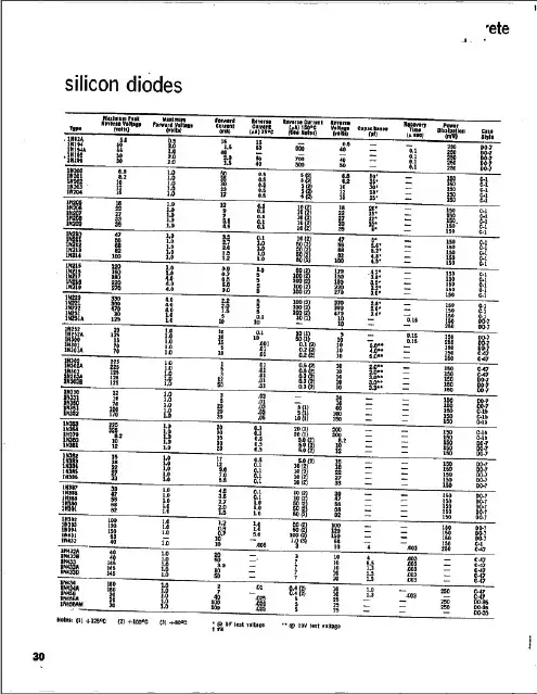
1N222中文资料
- 格式:pdf
- 大小:269.42 KB
- 文档页数:6
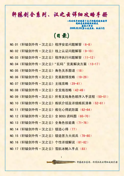
N0.01《轩辕剑外传·汉之云》程序安装问题解答(6-8)N0.02《轩辕剑外传·汉之云》线上认证问题解答(9-10)N0.03《轩辕剑外传·汉之云》程序执行问题解答(11-12)NO.04《轩辕剑外传·汉之云》“乱码”完美解决方案(13-17) NO.05《轩辕剑外传·汉之云》角色关系图谱(18)NO.06《轩辕剑外传·汉之云》完美剧情攻略(19-28)NO.07《轩辕剑外传·汉之云》主线攻略(29-41)NO.08《轩辕剑外传·汉之云》全支线攻略(42-49)NO.09《轩辕剑外传·汉之云》所有支线角色顺序入手流程(50-51)NO.10《轩辕剑外传·汉之云》炼妖介绍及详细炼妖清单(52-61)NO.11《轩辕剑外传·汉之云》炼化心得武防篇(62-64)NO.12《轩辕剑外传·汉之云》全BOSS资料图(65-70)NO.13《轩辕剑外传·汉之云》全角色技能表(71-76)NO.14《轩辕剑外传·汉之云》锻造心得(77)NO.15《轩辕剑外传·汉之云》锻造苦力大阅兵(78-80)NO.16《轩辕剑外传·汉之云》个性详细解说(81-82)NO.17《轩辕剑外传·汉之云》雪肌冰鲍入手点(83)1NO.18《轩辕剑外传·汉之云》白柳涧机关解法(84)NO.19《轩辕剑外传·汉之云》DOMO工作室全攻略(85-88)NO.20《轩辕剑一·倩女幽魂》详细介绍(89-90)N0.21《轩辕剑一·倩女幽魂》简明攻略(91)NO.22《轩辕剑二·壶中仙》详细介绍(92-93)N0.23《轩辕剑二·壶中仙》剧情攻略(94-95)N0.24《轩辕剑二·壶中仙》物品介绍(96-97)NO.25《轩辕剑二·壶中仙》奇术系统(98)NO.26《轩辕剑外传·枫之舞》详细介绍(99-100)NO.27《轩辕剑外传·枫之舞》完全攻略(101-105)NO.28《轩辕剑外传·枫之舞》心得及修改(106)NO.29《轩辕剑三·云和山的彼端》详细介绍(107)NO.30《轩辕剑三·云和山的彼端》完美文字攻略(108-116)NO.31《轩辕剑三·云和山的彼端》升级档支线攻略(117)NO.32《轩辕剑三·云和山的彼端》炼妖壶炼化表(118-121)NO.33《轩辕剑三·云和山的彼端》详细炼妖清单(122-131)NO.34《轩辕剑三·云和山的彼端》修改参数指南(132-135)2NO.35《轩辕剑三·云和山的彼端》小秘密全详解(136-137)NO.36《轩辕剑三·云和山的彼端》所有绝技及达成条件(138-139)NO.37《轩辕剑三·云和山的彼端》之超级商人撒尔达(140)NO.38《轩辕剑三·云和山的彼端》封印之剑之迷(141)NO.39《轩辕剑三外传·天之痕》详细介绍(142-143)NO.40《轩辕剑三外传·天之痕》详细攻略(144-148)NO.41《轩辕剑三外传·天之痕》完美修改大全(149-151)NO.42《轩辕剑三外传·天之痕》物品修改方法(152-153)NO.43《轩辕剑三外传·天之痕》炼妖壶宝典(154-161)NO.44《轩辕剑三外传·天之痕》符鬼饲养指南(162)NO.45《轩辕剑三外传·天之痕》偷窃一览表(163)NO.46《轩辕剑三外传·天之痕》女主角好感度详解(164)NO.47《轩辕剑三外传·天之痕》上古魔兽出现地方及条件(165)NO.48《轩辕剑三外传·天之痕》隐藏宝物(166-170)NO.49《轩辕剑三外传·天之痕》法宝详细位置(171-192)NO.50《轩辕剑战略版·轩辕伏魔录》详细介绍(193-194)NO.51《轩辕剑战略版·轩辕伏魔录》角色介绍(195)3NO.52《轩辕剑战略版·轩辕伏魔录》完美攻略(196-201)NO.53《轩辕剑战略版·轩辕伏魔录》之召唤神兽(202-203)NO.54《轩辕剑战略版·轩辕伏魔录》物品代码(204-206)NO.55《轩辕剑战略版·轩辕伏魔录》秘技(207)NO.56《轩辕剑战略版·轩辕伏魔录》中的DOMO工作室(208)NO.57《轩辕剑四·黑龙舞兮云飞扬》详细介绍(209-210)NO.58《轩辕剑四·黑龙舞兮云飞扬》剧情攻略(211-222)NO.59《轩辕剑四·黑龙舞兮云飞扬》资料片支线任务攻略(223-224)NO.60《轩辕剑四·黑龙舞兮云飞扬》可学法术列表(225-227)NO.61《轩辕剑四·黑龙舞兮云飞扬》天书居民修改(228)NO.62《轩辕剑四·黑龙舞兮云飞扬》之DOMO小组全代码(229)NO.63《轩辕剑外传·苍之涛》详细介绍(230-231)NO.64《轩辕剑外传·苍之涛》剧情攻略(232-243)NO.65《轩辕剑外传·苍之涛》修改全代码(244-245)NO.66《轩辕剑外传·苍之涛》仙术道场可学法术一览(246-251)NO.67《轩辕剑五·一剑凌云山海情》详细介绍(252)NO.68《轩辕剑五·一剑凌云山海情》详细攻略(253-257)4NO.69《轩辕剑五·一剑凌云山海情》各主角加入条件(258-260)NO.70《轩辕剑五·一剑凌云山海情》着火和冰冻树精(261)NO.71《轩辕剑五·一剑凌云山海情》28颗星曜石攻略(262)NO.72《轩辕剑五·一剑凌云山海情》角色实用度排行榜(263-264)NO.73《轩辕剑五·一剑凌云山海情》技能列表(265-267)NO.74《轩辕剑五·一剑凌云山海情》加速小法(268)NO.75《轩辕剑五·一剑凌云山海情》属性及物品代码(269-271)NO.76《轩辕剑五·一剑凌云山海情》全物品修改方法(272-275)NO.77《轩辕剑五·一剑凌云山海情》全任务清单(276-281)NO.78《轩辕剑全系列》经典对话及台词搜集(282-301)5N0.01《轩辕剑外传·汉之云》程序安装问题解答Q1:我家的计算机能不能玩轩辕剑外传-汉之云?A1:轩辕剑外传-汉之云官方网站与包装上均有载明系统基本&建议需求,请您先行阅读。

2N2218-2N22192N2221-2N2222January 1989HIGH-SPEED SWITCHESABSOLUTE MAXIMUM RATINGSSymbol ParameterValue Unit V CBO Collector-base Voltage (I E =0)60V V CEO Collector-emitter Voltage (I B =0)30V V EBO Emitter-base Voltage (I C =0)5V I C Collector Current0.8A P t o tTotal Power Dissipation at T amb ≤25°Cfor 2N2218and 2N2219for 2N2221and 2N2222at T c as e ≤25°C for 2N2218and 2N2219for 2N2221and 2N22220.80.531.8W W W W T st g Storage Temperature –65to 200°C T jJunction Temperature175°C DESCRIPTIONTO-18TO-39INTERNAL SCHEMATIC DIAGRAM2N2218/2N2219approved to CECC 50002-100,2N2221/2N2222approved to CECC 50002-101available on request.The 2N2218,2N2219,2N2221and 2N2222are sili-con planar epitaxial NPN transistors in Jedec TO-39(for 2N2218and 2N2219)and in Jedec TO-18(for 2N2221and 2N2222)metal cases.They are designed for high-speed switching applications at collector currents up to 500mA,and feature use-ful current gain over a wide range of collector cur-rent,low leakage currents and low saturation volt-ages.1/5ELECTRICAL CHARACTERISTICS (T amb =25°C unless otherwise specified)Symbol ParameterTest Conditions Min.Typ.Max.Unit I CBO Collector Cutoff Current (I E =0)V CB =50V V CB =50V T am b =150°C1010nA µA I E BO Emitter Cutoff Current (I C =0)V E B =3V 10nA V (BR)CBOColllector-base Breakdown Voltage (I E =0)I C =10µA 60V V (BR)CE O *Collector-emitter Breakdown Voltage (I B =0)I C =10mA 30V V (BR)EBOEmittter-base Breakdown Voltage (I C =0)I E =10µA 5VV CE (s at )*Collector-emitter Saturation VoltageI C =150mA I C =500mA I B =15mA I B =50mA 0.41.6V V V B E(s at )*Base-emitter Saturation VoltageI C =150mA I C =500mAI B =15mA I B =50mA 1.32.6V Vh F E *DC Current Gainfor 2N2218I C =0.1mA I C =1mA I C =10mA I C =150mA I C =500mA I C =150mA for 2N2219I C =0.1mA I C =1mA I C =10mA I C =150mA I C =500mA I C =150mA and 2N2221V CE =10V V CE =10V V CE =10V V CE =10V V CE =10V V CE =1V and 2N2222V CE =10V V CE =10V V CE =10V V CE =10V V CE =10V V CE =1V 2025354020203550751003050120300f T Transition Frequency I C =20mA f =100MHz V CE =20V 250MHz C CBO Collector-base Capacitance I E =0f =100kHz V CB =10V 8pF R e (h ie )Real Part of Input ImpedanceI C =20mA f =300MHzV CE =20V60Ω*Pulsed :pulse duration =300µs,duty cycle =1%.THERMAL DATA2N22182N22192N22212N2222R t h j-cas e R t h j-ambThermal Resistance Junction-case Thermal Resistance Junction-ambientMax Max50°C/W 187.5°C/W83.3°C/W 300°C/W2N2218-2N2219-2N2221-2N22222/5DIM.mminch MIN.TYP.MAX.MIN.TYP.MAX.A 12.70.500B 0.490.019D 5.30.208E 4.90.193F 5.80.228G 2.540.100H 1.20.047I 1.160.045L45o 45oLGI DAFE BHCTO-18MECHANICAL DATA00160432N2218-2N2219-2N2221-2N22223/5DIM.mminch MIN.TYP.MAX.MIN.TYP.MAX.A 12.70.500B 0.490.019D 6.60.260E 8.50.334F 9.40.370G 5.080.200H 1.20.047I 0.90.035L45o (typ.)LGI DAFE BHTO39MECHANICAL DATAP008B2N2218-2N2219-2N2221-2N22224/52N2218-2N2219-2N2221-2N2222 Information furnished is believed to be accurate and reliable.However,SGS-THOMSON Microelectronics assumes no responsability for the consequences of use of such information nor for any infringement of patents or other rights of third parties which may results from its use.No license is granted by implication or otherwise under any patent or patent rights of SGS-THOMSON Microelectronics.Specificationsmentioned in this publication are subject to change without notice.This publication supersedes and replaces all information previously supplied.SGS-THOMSON Microelectronics products are not authorized for use as critical components in life support devices or systems without express written approval of SGS-THOMSON Microelectonics.©1994SGS-THOMSON Microelectronics-All Rights ReservedSGS-THOMSON Microelectronics GROUP OF COMPANIESAustralia-Brazil-France-Germany-Hong Kong-Italy-Japan-Korea-Malaysia-Malta-Morocco-The Netherlands-Singapore-Spain-Sweden-Switzerland-Taiwan-Thailand-United Kingdom-U.S.A5/5。

Large Can Aluminum Electrolytic CapacitorsFEATURES• NEW SIZES FOR LOW PROFILE AND HIGH DENSITY DESIGN OPTIONS • EXPANDED CV VALUE RANGE• HIGH RIPPLE CURRENT• LONG LIFE • CAN-TOP SAFETY VENT• DESIGNED AS INPUT FILTER OF SMPS • STANDARD 10mm (.400") SNAP-IN SPACING NRLM SeriesSPECIFICATIONS(* 47,000µF add 0.14, 68,000µF add 0.35.)Notice for MountingThe space from the top of the can shall be more than (3mm) from chassis or other construction materials so that safety vent has room to expand in case of emer g en c y.Sleeve Color: DarkBlueCan Top Safety VentInsulation Sleeve and Minus Polarity Marking(4.0mm Leads Available As Option)D+1Max.L ± 26.3 ± 10.810(-)(+)MAXIMUM EX P AN S IONFOR SAFETY VENT Approx. 3.0mmRecommended PC Board Mounting Holes:10 ± .1∅= 2 ± 0.1D ∅ ± 0.5ChassisPC BoardPRECAUTIONSPlease review the notes on correct use, safety and precautions found on pages T10 & T11of NIC’s Electrolytic Capacitor catalog . Operating Temperature Range-40 ~ +85°C-25 ~ +85°C Rated Voltage Range 16 ~ 250Vdc 350 ~ 450Vdc Rated Capacitance Range 180 ~ 68,000µF56 ~ 680µFCapacitance Tolerance ±20% (M)Max. Leakage Current (µA)After 5 minutes (20°C)3 x C(µF)VMax. Tan δat 120Hz/20°C W.V. (Vdc)162535506380100160~450Tan δ max.0.50*0.40*0.350.300.250.200.200.15Surge VoltageW.V. (Vdc)162535506380100160S.V. (Vdc)2032446379100125200W.V. (Vdc)180200250350400450--S.V. (Vdc)220250300400450500--Ripple CurrentCorrection Factors Frequency (Hz)50601001205001K 10K ~ 50K -Multiplier at 85°C0.750.800.95 1.00 1.05 1.08 1.15-Low TemperatureStability (10 to 250Vdc)Temperature (°C)0-25-40-----Capacitance Change-5%-15%-30%-----Impedance Ratio 1.539-----Load Life Test2,000 hours at +85°CCapacitance ChangeWithin ±20% of initial measured value Tan δLess than 200% of specifi ed maximum valueLeakage Current Less than specifi ed maximum value Shelf Life Test1,000 hours at +85°C (no load)Capacitance Change Within ±20% of initial measured value Tan δLess than 200% of specifi ed maximum valueLeakage Current Less than specifi ed maximum value Surge Voltage Test Per JIS-C-5141 (table #6, #4)Surge voltage applied: 30 seconds"On" and 5.5 minutes no voltage "Off"Capacitance Change Within ±20% of initial measured value Tan δLess than 200% of specifi ed maximum valueLeakage Current Less than specifi ed maximum value Soldering EffectRefer to MIL-STD-202F Method 210A Capacitance Change Within ±10% of initial measured valueTan δLess than specifi ed maximum value Leakage CurrentLess than specifi ed maximum valueRoHS Compliantincludes all homogeneous materials*See Part Number System for DetailsLarge Can Aluminum Electrolytic CapacitorsNRLM SeriesNRLM 222 M 50V 20X25 FRoHS compliant Case Size (mm) Voltage Rating Tolerance Code PART NUMBER SYSTEMLarge Can Aluminum Electrolytic Capacitors NRLM Series STANDARD PRODUCT LIST, CASE SIZE AND SPECIFICATIONS。
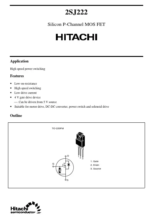
2SJ222Silicon P-Channel MOS FETApplicationHigh speed power switchingFeatures• Low on-resistance• High speed switching• Low drive current• 4 V gate drive deviceCan be driven from 5 V source• Suitable for motor drive, DC-DC converter, power switch and solenoid drive Outline2SJ2222Absolute Maximum Ratings (Ta = 25°C)ItemSymbol Ratings Unit Drain to source voltage V DSS –100V Gate to source voltage V GSS ±20V Drain current I D–20A Drain peak currentI D(pulse)*1–80A Body to drain diode reverse drain current I DR –20A Channel dissipation Pch*235W Channel temperature Tch 150°C Storage temperatureTstg–55 to +150°CNotes: 1.PW ≤ 10 µs, duty cycle ≤ 1%2.Value at T C = 25°C2SJ2223Electrical Characteristics (Ta = 25°C)ItemSymbol Min Typ Max Unit Test conditions Drain to source breakdown voltageV (BR)DSS –100——V I D = –10 mA, V GS = 0Gate to source breakdown voltageV (BR)GSS ±20——V I G = ±100 µA, V DS = 0Gate to source leak current I GSS ——±10µA V GS = ±16 V, V DS = 0Zero gate voltage drain current I DSS——–250µA V DS = –80 V, V GS = 0Gate to source cutoff voltage V GS(off)–1.0—–2.0V I D = –1 mA, V DS = –10 V Static drain to source on state R DS(on)—0.120.16ΩI D = –10 A, V GS = –10 V*1resistance—0.160.22I D = –10 A, V GS = –4 V*1Forward transfer admittance |y fs |7.512—S I D = –10 A, V DS = –10 V*1Input capacitance Ciss —1800—pF V DS = –10 V, V GS = 0,Output capacitanceCoss —680—pF f = 1 MHzReverse transfer capacitance Crss —145—pF Turn-on delay time t d(on)—15—ns I D = –10 A, V GS = –10 V,Rise timet r —115—ns R L = 3 ΩTurn-off delay time t d(off)—320—ns Fall timet f —170—ns Body to drain diode forward voltageV DF —–1.05—V I F = –20 A, V GS = 0Body to drain diode reverse recovery time t rr—280—nsI F = –20 A, V GS = 0,di F /dt = 50 A/µs Note:1.Pulse testSee characteristic curves of 2SJ2212SJ2224Cautions1.Hitachi neither warrants nor grants licenses of any rights of Hitachi’s or any third party’s patent,copyright, trademark, or other intellectual property rights for information contained in this document.Hitachi bears no responsibility for problems that may arise with third party’s rights, includingintellectual property rights, in connection with use of the information contained in this document.2.Products and product specifications may be subject to change without notice. Confirm that you have received the latest product standards or specifications before final design, purchase or use.3.Hitachi makes every attempt to ensure that its products are of high quality and reliability. However,contact Hitachi’s sales office before using the product in an application that demands especially high quality and reliability or where its failure or malfunction may directly threaten human life or cause risk of bodily injury, such as aerospace, aeronautics, nuclear power, combustion control, transportation,traffic, safety equipment or medical equipment for life support.4.Design your application so that the product is used within the ranges guaranteed by Hitachi particularly for maximum rating, operating supply voltage range, heat radiation characteristics, installationconditions and other characteristics. Hitachi bears no responsibility for failure or damage when used beyond the guaranteed ranges. Even within the guaranteed ranges, consider normally foreseeable failure rates or failure modes in semiconductor devices and employ systemic measures such as fail-safes, so that the equipment incorporating Hitachi product does not cause bodily injury, fire or other consequential damage due to operation of the Hitachi product.5.This product is not designed to be radiation resistant.6.No one is permitted to reproduce or duplicate, in any form, the whole or part of this document without written approval from Hitachi.7.Contact Hitachi’s sales office for any questions regarding this document or Hitachi semiconductor products.Hitachi, Ltd.Semiconductor & Integrated Circuits.Nippon Bldg., 2-6-2, Ohte-machi, Chiyoda-ku, Tokyo 100-0004, Japan Tel: Tokyo (03) 3270-2111 Fax: (03) 3270-5109Copyright ' Hitachi, Ltd., 1999. All rights reserved. Printed in Japan.Hitachi Asia Pte. Ltd.16 Collyer Quay #20-00Hitachi TowerSingapore 049318Tel: 535-2100Fax: 535-1533URLNorthAmerica : http:/Europe : /hel/ecg Asia (Singapore): .sg/grp3/sicd/index.htm Asia (Taiwan): /E/Product/SICD_Frame.htm Asia (HongKong): /eng/bo/grp3/index.htm Japan : http://www.hitachi.co.jp/Sicd/indx.htmHitachi Asia Ltd.Taipei Branch Office3F, Hung Kuo Building. No.167, Tun-Hwa North Road, Taipei (105)Tel: <886> (2) 2718-3666Fax: <886> (2) 2718-8180Hitachi Asia (Hong Kong) Ltd.Group III (Electronic Components)7/F., North Tower, World Finance Centre,Harbour City, Canton Road, Tsim Sha Tsui,Kowloon, Hong Kong Tel: <852> (2) 735 9218Fax: <852> (2) 730 0281 Telex: 40815 HITEC HXHitachi Europe Ltd.Electronic Components Group.Whitebrook ParkLower Cookham Road MaidenheadBerkshire SL6 8YA, United Kingdom Tel: <44> (1628) 585000Fax: <44> (1628) 778322Hitachi Europe GmbHElectronic components Group Dornacher Stra§e 3D-85622 Feldkirchen, Munich GermanyTel: <49> (89) 9 9180-0Fax: <49> (89) 9 29 30 00Hitachi Semiconductor (America) Inc.179 East Tasman Drive,San Jose,CA 95134 Tel: <1> (408) 433-1990Fax: <1>(408) 433-0223For further information write to:。