K34100W1EN1S中文资料
- 格式:pdf
- 大小:276.92 KB
- 文档页数:3

NAS 系列交流伺服系统使用说明书特别提示在您第一次接通本伺服系统电源以前,为确保系统能安全、正常、高效地为您工作,请仔细阅读手册中有关使用方面的重要信息。
感谢使用星辰伺服的交流伺服系统!为使本机一直维持良好的运行状态,请将本手册随整机附送给最终用户。
虽然在您的选型过程中,可能已经对本产品有所了解并与本公司的技术人员进行了某些沟通,但为充分发挥本机最佳功能,仍请在使用前,仔细阅读本使用说明书,必要时可与星辰伺服的有关人员联系以获得必要的帮助。
本说明书中,对不同级别的提示、警示、警告采用如下提示符:★一般性的提示警示,如果不按照执行,可能带来设备的损坏警告,如果不按照执行可能带来设备严重损坏、火灾或人身伤害星辰伺服分支机构及技术服务机构:桂林星辰电力电子有限公司市场服务部地址:桂林高新技术产业开发区星辰大厦邮编:541004电话:************,5810692 传真:************ Email:******************上海星之辰电气传动技术有限公司伺服部地址:上海市科技创业中心(徐汇区钦州路100号)2#601-605 邮编:200235电话:************(8线), 64829055 传真:************深圳市星辰激光技术有限公司伺服部地址:深圳市高新区北区清华信息港研发楼A栋3楼邮编:518057电话:*************(15线),26030572 传真:*************目录1.安全注意事项1.1.安装注意事项1.2.运转操作注意事项1.3.保养检查注意事项1.4.关于废弃1.5.其它2.产品的确认和注意事项2.1.产品的确认2.2.伺服电机型号说明2.3.伺服驱动器型号说明2.4.使用前的注意事项3.NAS系列交流伺服系统性能参数3.1.NAS系列伺服系统标准规格配套表3.2.驱动器标准规格及功能表3.2.1.驱动器标准规格及一般功能3.2.2.驱动器使用环境条件及一般技术状态3.2.3.驱动器控制功能及运动性能表3.2.4.伺服电机特性3.2.4.1.N系列电机3.2.4.2.SY系列电机3.2.5.有关工作制的说明4.安装4.1.安装场所和保养4.2.驱动器外形尺寸4.3.驱动器安装4.4.驱动器前级盒的拆卸和安装4.5.伺服电机外形尺寸4.6.伺服电机安装4.7.制动电阻安装5.端口说明及外围电路设计5.1.接线注意事项5.2.外围接线图及端口说明5.2.1.控制接口(44芯排插头)全部功能连接图5.2.2.控制接口(44芯排插头)接口功能表5.2.3.状态通报口的使用5.2.4.模拟量接口的使用5.2.5.转矩环控制运行5.2.6.速度环控制运行5.2.7.带速度限制的位置环控制运行5.2.8.带转矩限制的位置环控制运行5.2.9.带转矩限制的速度环控制运行5.2.10.带转矩偏置的速度环控制运行5.2.11.位置环脉冲给定接口的使用5.2.12.反馈接口(15芯排插头)的连接5.2.13.反馈接口(15芯排插头)端口功能表5.2.14. RS485接口(9芯排插头)的连接5.2.15. RS485接口(9芯排插头)端口功能表5.2.16.动力接口6.操作面板6.1.面板显示说明6.1.1.监视状态下驱动器面板显示状态表6.1.2.运行状态下驱动器面板显示状态表6.2.面板操作说明及编辑状态下面板显示6.2.1.几种典型的操作6.2.2.编辑状态下的显示7.运转7.1.运转前的检查7.2.首次上电和试运转7.3.运转7.3.1.功能、参数设定总表7.3.2.位置闭环运行7.3.3.速度闭环运行7.3.4.转矩环运行8.RS485串行通讯功能8.1.概述8.2.通过RS485串行通讯进行伺服驱动器的运转8.2.1.状态查询8.2.2.修改参数8.2.3.实时控制8.3.TB485-V10通讯协议8.3.1.串口通讯数据格式8.3.2.工作方式说明8.3.2.1.问答方式8.3.2.2.速传方式8.3.3.通讯故障约定及校验说明8.3.3.1.问答方式8.3.3.2.速传方式9.保护功能9.1.设定方法(功能代码显示模式)9.2.功能代码一览表9.3.功能说明10.故障确认11.保养和检查11.1.保养和检查时的注意事项11.2.检查项目11.3.兆欧表测试11.4.零部件的更换安全注意事项1.安全注意事项1.1.安装注意事项★ 安装环境:使用温度伺服电机 -20℃~+40℃伺服驱动器 -10℃~+40℃保存温度-25℃~+65℃环境湿热伺服电机 95%,30℃,不结露伺服驱动器 90%,30℃,不结露标准高度海拔2000m以下(2000m以上,每上升1000m降容20%)★ 请将电机和驱动器安装于通风良好的场所。

元器件交易网ASAHI KASEI[AK4628A]AK4628AHigh Performance Multi-channel Audio CODECGENERAL DESCRIPTION The AK4628A is a single chip CODEC that includes two channels of ADC and eight channels of DAC. The ADC outputs 24bit data and the DAC accepts up to 24bit input data. The ADC has the Enhanced Dual Bit architecture with wide dynamic range. The DAC introduces the newly developed Advanced Multi-Bit architecture, and achieves wider dynamic range and lower outband noise. An auxiliary digital audio input interface maybe used instead of the ADC for passing audio data to the primary audio output port. Control may be set directly by pins or programmed through a separate serial interface. The AK4628A has a dynamic range of 102dB for ADC, 106dB for DAC and is well suited for digital surround for home theater and car audio. An AC-3 system can be built with a IEC60958(SPDIF) receiver such as the AK4112B. The AK4628A is available in a small 44pin LQFP package which will reduce system space.*AC-3 is a trademark of Dolby Laboratories.FEATURES 2ch 24bit ADC - 64x Oversampling - Sampling Rate up to 96kHz - Linear Phase Digital Anti-Alias Filter - Single-Ended Input - S/(N+D): 92dB - Dynamic Range, S/N: 102dB - Digital HPF for offset cancellation - I/F format: MSB justified, I2S or TDM - Overflow flag 8ch 24bit DAC - 128x Oversampling - Sampling Rate up to 192kHz - 24bit 8 times Digital Filter - Single-Ended Outputs - On-chip Switched-Capacitor Filter - S/(N+D): 90dB - Dynamic Range, S/N: 106dB - I/F format: MSB justified, LSB justified(20bit,24bit), I2S or TDM - Individual channel digital volume with 128 levels and 0.5dB step - Soft mute - De-emphasis for 32kHz, 44.1kHz and 48kHz - Zero Detect Function High Jitter Tolerance TTL Level Digital I/F 3-wire Serial and I2C Bus µP I/F for mode setting Master clock:256fs, 384fs or 512fs for fs=32kHz to 48kHz 128fs, 192fs or 256fs for fs=64kHz to 96kHz 128fs for fs=120kHz to 192kHz Power Supply: 4.5 to 5.5V Power Supply for output buffer: 2.7 to 5.5V Small 44pin LQFP AK4529 Pin CompatibleMS0385-E-00 -1-2005/02元器件交易网ASAHI KASEI[AK4628A]Block DiagramLINADC ADCHPF HPFAudio I/FRINRX1 RX2 RX3 RX4 XTILOUT1LPFDACDATTMCLK LRCK BICKMCLK LRCK BICK DAUXXTO MCKO LRCK BICK SDTODIR AK4112BROUT1LPFDACDATTLOUT2LPFDACDATTFormat ConverterROUT2LPFDACDATTSDOUT SDOS SDTO LRCK BICK SDIN SDOUT1 SDOUT2 SDOUT3 SDOUT4AC3LOUT3LPFDACDATTSDIN1 SDIN2 SDIN3 SDIN4ROUT3LPFDACDATTSDTI1 SDTI2 SDTI3 SDTI4LOUT4LPFDACDATTROUT4LPFDACDATTAK4628ABlock Diagram (DIR and AC-3 DSP are external parts)MS0385-E-00 -2-2005/02元器件交易网ASAHI KASEI[AK4628A]Ordering GuideAK4628AVQ AKD4628 -40 ∼ +85°C 44pin LQFP(0.8mm pitch) Evaluation Board for AK4628APin LayoutLOOP0/SDA/CDTIDIF1/SCL/CCLKDIF0/CSNVREFH 35MCLK444143424037AVSSAVDDDZF1P/S3938SDOS I2C SMUTE BICK LRCK SDTI1 SDTI2 SDTI3 SDTO DAUX DFS01 2 3 4 5 6 7 8 9 10 11 12 13 14 15 16 17 18 19 20 21 22 Top View3634 33 32 31VCOMTDM0DZF2/OVF RIN LIN NC TST2 ROUT1 LOUT1 ROUT2 LOUT2 ROUT3 LOUT3AK4628AVQ30 29 28 27 26 25 24 23MS0385-E-00 -3-ROUT4LOUT4SDTI4DVDDDVSSTVDDCAD1CAD0DZFETST1PDN2005/02元器件交易网ASAHI KASEI[AK4628A]Compatibility with AK45291. Functions Functions DAC Sampling frequency TDM128 (96kHz) Digital Attenuator Soft Mute DAC channel power-downAK4529 Up to 96kHz Not available 256 levels Soft mute function is independent of Digital attenuator. Not availableAK4628A Up to 192kHz Available 128 levels Soft mute function is not independent of Digital attenuator. Available2. Pin Configuration pin# 11 18 29 44AK4529 DFS TST NC TDMAK4628A DFS0 TST1 TST2 TDM03. Register Addr 00H 00H 01H 01H 01H 09HAK4529 TDM Not available DFS Not available Not available Not availableAK4628A TDM0 TDM1 DFS0 DFS1 CKS1, CKS0 PD4, PD3, PD2, PD1MS0385-E-00 -4-2005/02元器件交易网ASAHI KASEI[AK4628A]PIN/FUNCTIONNo. 1 Pin Name SDOS I/O I Function SDTO Source Select Pin (Note 1) “L”: Internal ADC output, “H”: DAUX input SDOS pin should be set to “L” when TDM= “1”. Control Mode Select Pin “L”: 3-wire Serial, “H”: I2C Bus Soft Mute Pin (Note 1) When this pin goes to “H”, soft mute cycle is initialized. When returning to “L”, the output mute releases. Audio Serial Data Clock Pin Input Channel Clock Pin DAC1 Audio Serial Data Input Pin DAC2 Audio Serial Data Input Pin DAC3 Audio Serial Data Input Pin Audio Serial Data Output Pin AUX Audio Serial Data Input Pin Double Speed Sampling Mode Pin (Note 1) “L”: Normal Speed, “H”: Double Speed DAC4 Audio Serial Data Input Pin Zero Input Detect Enable Pin “L”: mode 7 (disable) at parallel mode, zero detect mode is selectable by DZFM3-0 bits at serial mode “H”: mode 0 (DZF1 is AND of all eight channels) Output Buffer Power Supply Pin, 2.7V∼5.5V Digital Power Supply Pin, 4.5V∼5.5V Digital Ground Pin, 0V Power-Down & Reset Pin When “L”, the AK4628A is powered-down and the control registers are reset to default state. If the state of P/S or CAD1-0 changes, then the AK4628A must be reset by PDN. Test Pin This pin should be connected to DVSS. Chip Address 1 Pin Chip Address 0 Pin DAC4 Lch Analog Output Pin DAC4 Rch Analog Output Pin2 3I2C SMUTEI I4 5 6 7 8 9 10 11 12 13BICK LRCK SDTI1 SDTI2 SDTI3 SDTO DAUX DFS0 SDTI4 DZFEI I I I I O I I I I14 15 16 17TVDD DVDD DVSS PDNI18 19 20 21 22TST1 CAD1 CAD0 LOUT4 ROUT4I I I O OMS0385-E-00 -5-2005/02元器件交易网ASAHI KASEI[AK4628A]No. 23 24 25 26 27 28 29 30 31 32 33Pin Name LOUT3 ROUT3 LOUT2 ROUT2 LOUT1 ROUT1 TST2 NC LIN RIN DZF2I/O O O O O O O I I I OFunction DAC3 Lch Analog Output Pin DAC3 Rch Analog Output Pin DAC2 Lch Analog Output Pin DAC2 Rch Analog Output Pin DAC1 Lch Analog Output Pin DAC1 Rch Analog Output Pin Test pin (Internal pull-down pin) This pin should be left floating or connected to AVSS. No Connect No internal bonding. Lch Analog Input Pin Rch Analog Input Pin Zero Input Detect 2 Pin (Note 2) When the input data of the group 1 follow total 8192 LRCK cycles with “0” input data, this pin goes to “H”. And when RSTN bit is “0”, PWDAN pin is “0”, this pin goes to “H”. It always is in “L” when P/S is “H”. Analog Input Overflow Detect Pin (Note 3) This pin goes to “H” if the analog input of Lch or Rch overflows. Common Voltage Output Pin, AVDD/2 Large external capacitor around 2.2µF is used to reduce power-supply noise. Positive Voltage Reference Input Pin, AVDD Analog Power Supply Pin, 4.5V∼5.5V Analog Ground Pin, 0V Zero Input Detect 1 Pin (Note 2) When the input data of the group 1 follow total 8192 LRCK cycles with “0” input data, this pin goes to “H”. And when RSTN bit is “0”, PWDAN pin is “0”, this pin goes to “H”. Output is selected by setting DZFE pin when P/S is “H”. Master Clock Input Pin Parallel/Serial Select Pin “L”: Serial control mode, “H”: Parallel control mode Audio Data Interface Format 0 Pin in parallel control mode Chip Select Pin in 3-wire serial control mode This pin should be connected to DVDD at I2C bus control mode Audio Data Interface Format 1 Pin in parallel control mode Control Data Clock Pin in serial control mode I2C = “L”: CCLK (3-wire Serial), I2C = “H”: SCL (I2C Bus) Loopback Mode 0 Pin in parallel control mode Enables digital loop-back from ADC to 4 DACs. Control Data Input Pin in serial control mode I2C = “L”: CDTI (3-wire Serial), I2C = “H”: SDA (I2C Bus) TDM I/F Format Mode Pin (Note 1) “L”: Normal mode, “H”: TDM modeOVF 34 35 36 37 38 VCOM VREFH AVDD AVSS DZF1O O I O39 40 41MCLK P/S DIF0 CSN DIF1 SCL/CCLK LOOP0 SDA/CDTII I I I I I I I/O I424344TDM0Notes: 1. SDOS, SMUTE, DFS0, and TDM0 pins are ORed with register data if P/S = “L”. 2. The group 1 and 2 can be selected by DZFM3-0 bits if P/S = “L” and DZFE = “L”. 3. This pin becomes OVF pin if OVFE bit is set to “1” at serial control mode. 4. All digital input pins except for pull-down should not be left floating.MS0385-E-00 -6-2005/02元器件交易网ASAHI KASEI[AK4628A]ABSOLUTE MAXIMUM RATINGS (AVSS, DVSS=0V; Note 5) Parameter Symbol min AVDD -0.3 Power Supplies Analog DVDD -0.3 Digital TVDD -0.3 Output buffer |AVSS-DVSS| (Note 6) ∆GND Input Current (any pins except for supplies) IIN Analog Input Voltage VINA -0.3 Digital Input Voltage (Expect LRCK, BICK pins) VIND1 -0.3 (LRCK, BICK pins) VIND2 -0.3 Ambient Temperature (power applied) Ta -40 Storage Temperature Tstg -65Notes: 5. All voltages with respect to ground. 6. AVSS and DVSS must be connected to the same analog ground plane.max 6.0 6.0 6.0 0.3 ±10 AVDD+0.3 DVDD+0.3 TVDD+0.3 85 150Units V V V V mA V V V °C °CWARNING: Operation at or beyond these limits may result in permanent damage to the device. Normal operation is not guaranteed at these extremes.RECOMMENDED OPERATING CONDITIONS (AVSS, DVSS=0V; Note 5) Parameter Symbol min typ Power Supplies Analog AVDD 4.5 5.0 (Note 7) Digital DVDD 4.5 5.0 Output buffer TVDD 2.7 5.0max 5.5 5.5 5.5Units V V VNotes: 5. All voltages with respect to ground. 7. The power up sequence between AVDD, DVDD and TVDD is not critical. Do not turn off only the AK4628A under the condition that a surrounding device is powered on and the I2C bus is in use. WARNING: AKM assumes no responsibility for the usage beyond the conditions in this datasheet.MS0385-E-00 -7-2005/02元器件交易网ASAHI KASEI[AK4628A]ANALOG CHARACTERISTICS (Ta=25°C; AVDD, DVDD, TVDD=5V; AVSS, DVSS=0V; VREFH=AVDD; fs=48kHz; BICK=64fs; Signal Frequency=1kHz; 24bit Data; Measurement Frequency=20Hz∼20kHz at 48kHz, 20Hz~40kHz at fs=96kHz, 20Hz~40kHz at fs=192kHz; unless otherwise specified) Parameter min typ max Units ADC Analog Input Characteristics Resolution 24 Bits S/(N+D) (-0.5dBFS) fs=48kHz 84 92 dB fs=96kHz 86 dB DR (-60dBFS) fs=48kHz, A-weighted 94 102 dB fs=96kHz 88 96 dB fs=96kHz, A-weighted 93 102 dB dB 102 94 S/N (Note 8) fs=48kHz, A-weighted dB 96 88 fs=96kHz dB 102 93 fs=96kHz, A-weighted Interchannel Isolation 90 110 dB DC Accuracy Interchannel Gain Mismatch 0.2 0.3 dB Gain Drift 20 ppm/°CInput Voltage AIN=0.62xVREFH 2.90 3.10 3.30 VppInput Resistance (Note 9) Power Supply Rejection (Note 10) DAC Analog Output Characteristics Resolution S/(N+D) fs=48kHz fs=96kHz fs=192kHz DR (-60dBFS) fs=48kHz, A-weighted fs=96kHz fs=96kHz, A-weightedfs=192kHz fs=192kHz, A-weighted1525 50 24kΩ dB Bits dB dB dB dB dB dB dB dB dB dB dB dB dB dB dB ppm/°C Vpp kΩ dBS/N(Note 11)fs=48kHz, A-weighted fs=96kHz fs=96kHz, A-weightedfs=192kHz fs=192kHz, A-weightedInterchannel Isolation DC Accuracy Interchannel Gain Mismatch Gain Drift Output Voltage AOUT=0.6xVREFH Load Resistance Power Supply Rejection Notes:80 78 95 88 94 95 88 94 9090 88 88 106 100 106 100 106 106 100 106 100 106 110 0.2 20 3.0 50 0.5 3.252.75 5 (Note 10)8. S/N measured by CCIR-ARM is 98dB(@fs=48kHz). 9. Input resistance is 16kΩ typically at fs=96kHz. 10. PSR is applied to AVDD, DVDD and TVDD with 1kHz, 50mVpp. VREFH pin is held a constant voltage. 11. S/N measured by CCIR-ARM is 102dB(@fs=48kHz).MS0385-E-00 -8-2005/02元器件交易网ASAHI KASEI[AK4628A]Parameter Power Supplies Power Supply Current (AVDD+DVDD+TVDD) Normal Operation (PDN = “H”) AVDD fs=48kHz, 96kHz fs=192kHz DVDD+TVDD fs=48kHz fs=96kHz fs=192kHz Power-down mode (PDN = “L”)mintypmaxUnits(Note 12)(Note 13)45 34 18 24 27 8067 51 27 36 40 200mA mA mA mA mA µANotes: 12. TVDD=0.1mA(typ). 13. In the power-down mode. All digital input pins including clock pins (MCLK, BICK, LRCK) are held DVSS.MS0385-E-00 -9-2005/02元器件交易网ASAHI KASEI[AK4628A]FILTER CHARACTERISTICS (Ta=25°C; AVDD, DVDD=4.5∼5.5V; TVDD=2.7∼5.5V; fs=48kHz) Parameter Symbol min ADC Digital Filter (Decimation LPF): PB 0 Passband (Note 14) ±0.1dB -0.2dB -3.0dB Stopband SB 28 Passband Ripple PR Stopband Attenuation SA 68 Group Delay (Note 15) GD Group Delay Distortion ∆GD ADC Digital Filter (HPF): Frequency Response (Note 14) -3dB FR -0.1dB DAC Digital Filter: Passband (Note 14) -0.1dB PB 0 -6.0dB Stopband SB 26.2 Passband Ripple PR Stopband Attenuation SA 54 Group Delay (Note 15) GD DAC Digital Filter + Analog Filter: FR Frequency Response: 0 ∼ 20.0kHz FR 40.0kHz (Note 16) FR 80.0kHz (Note 16)typmax 18.9 ±0.04Units kHz kHz kHz kHz dB dB 1/fs µs Hz Hz20.0 23.016 0 1.0 6.5 21.8 ±0.02 19.2 ±0.2 ±0.3 ±1.024.0kHz kHz kHz dB dB 1/fs dB dB dBNotes: 14. The passband and stopband frequencies scale with fs. For example, 21.8kHz at –0.1dB is 0.454 x fs. 15. The calculating delay time which occurred by digital filtering. This time is from setting the input of analog signal to setting the 24bit data of both channels to the output register for ADC. For DAC, this time is from setting the 20/24bit data of both channels on input register to the output of analog signal. 16. 40.0kHz; fs=96kHz , 80.0kHz; fs=192kHz.DC CHARACTERISTICS (Ta=25°C; AVDD, DVDD=4.5∼5.5V; TVDD=2.7∼5.5V) Parameter Symbol min High-Level Input Voltage VIH 2.2 Low-Level Input Voltage VIL High-Level Output Voltage TVDD-0.5 VOH (SDTO, LRCK, BICK pins: Iout=-100µA) AVDD-0.5 VOH (DZF1, DZF2/OVF pins: Iout=-100µA) Low-Level Output Voltage VOL (SDTO, LRCK, BICK,DZF1, DZF2/OVF pins: Iout= 100µA) VOL (SDA pins: Iout= 3mA) Input Leakage Current (Note 17) Iin Note 17: TST2 pin has an internal pull-down device, nominally 100kohm.typ -max 0.8 0.5 0.4 ±10Units V V V V V V µAMS0385-E-00 - 10 -2005/02SWITCHING CHARACTERISTICS(Ta=25°C; AVDD, DVDD=4.5∼5.5V; TVDD=2.7∼5.5V; C L=20pF)Parameter SymbolmintypmaxUnits Master Clock Timing256fsn, 128fsd: Pulse Width Low Pulse Width High 384fsn, 192fsd: Pulse Width Low Pulse Width High 512fsn, 256fsd: Pulse Width Low Pulse Width High fCLKtCLKLtCLKHfCLKtCLKLtCLKHfCLKtCLKLtCLKH8.192272712.288202016.384151512.28818.43224.576MHznsnsMHznsnsMHznsnsLRCK TimingNormal mode (TDM0= “0”, TDM1= “0”)Normal Speed Mode Double Speed Mode Quad Speed Mode Duty Cycle fsnfsdfsqDuty326412045489619255kHzkHzkHz%TDM256 mode (TDM0= “1”, TDM1= “0”)LRCK frequency “H” time“L” time fsntLRHtLRL321/256fs1/256fs48 kHznsnsTDM128 mode (TDM0= “1”, TDM1= “1”)LRCK frequency “H” time“L” time fsntLRHtLRL641/128fs1/128fs96 kHznsnsAudio Interface TimingNormal mode (TDM0= “0”, TDM1= “0”)BICK PeriodBICK Pulse Width LowPulse Width HighLRCK Edge to BICK “↑” (Note 18) BICK “↑” to LRCK Edge (Note 18) LRCK to SDTO(MSB)BICK “↓” to SDTOSDTI1-4,DAUX Hold TimeSDTI1-4,DAUX Setup Time tBCKtBCKLtBCKHtLRBtBLRtLRStBSDtSDHtSDS813232202020204040nsnsnsnsnsnsnsnsnsnsTDM256 mode (TDM0= “1”, TDM1= “0”)BICK PeriodBICK Pulse Width LowPulse Width HighLRCK Edge to BICK “↑” (Note 18) BICK “↑” to LRCK Edge (Note 18) BICK “↓” to SDTOSDTI1 Hold TimeSDTI1 Setup Time tBCKtBCKLtBCKHtLRBtBLRtBSDtSDHtSDS8132322020101020nsnsnsnsnsnsnsnsnsTDM128 mode (TDM0= “1”, TDM1= “1”)BICK PeriodBICK Pulse Width LowPulse Width HighLRCK Edge to BICK “↑” (Note 18) BICK “↑” to LRCK Edge (Note 18) BICK “↓” to SDTOSDTI1-2 Hold TimeSDTI1-2 Setup Time tBCKtBCKLtBCKHtLRBtBLRtBSDtSDHtSDS8132322020101020nsnsnsnsnsnsnsnsnsNotes: 18. BICK rising edge must not occur at the same time as LRCK edge.Parameter SymbolmintypmaxUnitsControl Interface Timing (3-wire Serial mode):CCLK PeriodCCLK Pulse Width LowPulse Width High CDTI Setup Time CDTI Hold TimeCSN “H” TimeCSN “↓” to CCLK “↑” CCLK “↑” to CSN “↑” tCCKtCCKLtCCKHtCDStCDHtCSWtCSStCSH200808040401505050nsnsnsnsnsnsnsnsControl Interface Timing (I2C Bus mode):SCL Clock FrequencyBus Free Time Between TransmissionsStart Condition Hold Time (prior to first clock pulse) Clock Low TimeClock High TimeSetup Time for Repeated Start ConditionSDA Hold Time from SCL Falling (Note 19) SDA Setup Time from SCL RisingRise Time of Both SDA and SCL LinesFall Time of Both SDA and SCL LinesSetup Time for Stop ConditionPulse Width of Spike Noise Suppressed by Input Filter fSCLtBUFtHD:STAtLOWtHIGHtSU:STAtHD:DATtSU:DATtRtFtSU:STOtSP-4.74.04.74.04.70.25--4.0100-------1.00.3-50kHzµsµsµsµsµsµsµsµsµsµsnsPower-down & Reset TimingPDN Pulse Width (Note 20) PDN “↑” to SDTO valid (Note 21) tPDtPDV150522ns1/fsNotes: 19. Data must be held for sufficient time to bridge the 300 ns transition time of SCL.20. The AK4628A can be reset by bringing PDN “L” to “H” upon power-up.21. These cycles are the number of LRCK rising from PDN rising.22. I2C is a registered trademark of Philips Semiconductors.Timing DiagramVIHMCLKVILLRCKVIH VILVIH BICKVILClock Timing (TDM= “0”)VIH MCLKVILLRCKVIH VILVIH BICKVILClock Timing (TDM= “1”)LRCKVIH BICKVILSDTO50%TVDDVIH VILSDTIVIH VILAudio Interface Timing (TDM= “0”)LRCKVIH BICKVILSDTO50%TVDDVIH VILSDTIVIH VILAudio Interface Timing (TDM= “1”)CSNVIH CCLKVILVIH CDTI VILVIHVILWRITE Command Input Timing (3-wire Serial mode)CSNVIH CCLKVILVIH CDTI VILVIHVILD3D2D1D0WRITE Data Input Timing (3-wire Serial mode)VIHVILVIHVILI 2C Bus mode TimingVILPDNSDTO 50%TVDDVIHPower-down & Reset TimingOPERATION OVERVIEWSystem ClockThe external clocks, which are required to operate the AK4628A, are MCLK, LRCK and BICK. MCLK should be synchronized with LRCK but the phase is not critical. There are two methods to set MCLK frequency. In Manual Setting Mode (ACKS = “0”: Default), the sampling speed is set by DFS0, DFS1 (Table 1). The frequency of MCLK at each sampling speed is set automatically. (Table 2, 3, 4). In Auto Setting Mode (ACKS = “1”), as MCLK frequency is detected automatically (Table 5), and the internal master clock becomes the appropriate frequency (Table 6), it is not necessary to set DFS.External clocks (MCLK, BICK) should always be present whenever the AK4628A is in normal operation mode (PDN = “H”). If these clocks are not provided, the AK4628A may draw excess current because the device utilizes dynamic refreshed logic internally. If the external clocks are not present, the AK4628A should be in the power-down mode (PDN = “L”) or in the reset mode (RSTN = “0”). After exiting reset at power-up etc., the AK4628A is in the power-down mode until MCLK and LRCK are input.(fs)SpeedDFS1 DFS0 SamplingDefaultMode 32kHz~48kHzSpeed0 0 Normal0 1 DoubleMode 64kHz~96kHzSpeedMode 120kHz~192kHz1 0 QuadSpeedTable 1. Sampling Speed (Manual Setting Mode)(MHz) BICK(MHz) LRCK MCLKfs 256fs 384fs 512fs 64fs32.0kHz 8.1920 12.2880 16.3840 2.048044.1kHz 11.2896 16.9344 22.5792 2.822448.0kHz 12.2880 18.4320 24.5760 3.0720Table 2. System Clock Example (Normal Speed Mode @Manual Setting Mode)LRCK MCLK (MHz) BICK (MHz)fs 128fs 192fs 256fs 64fs88.2kHz 11.2896 16.9344 22.5792 5.644896.0kHz 12.2880 18.4320 24.5760 6.1440Table 3. System Clock Example (Double Speed Mode @Manual Setting Mode) (Note: At Double speed mode(DFS1= “0”, DFS0 = “1”), 128fs and 192fs are not available for ADC.)LRCK MCLK (MHz) BICK (MHz)fs 128fs 192fs 256fs 64fs176.4kHz 22.5792 - - 11.2896192.0kHz 24.5760 - - 12.2880Table 4. System Clock Example (Quad Speed Mode @Manual Setting Mode)(Note: At Quad speed mode(DFS1= “1”, DFS0 = “0”) are not available for ADC.)MCLK Sampling Speed512fs Normal 256fs Double 128fs QuadTable 5. Sampling Speed (Auto Setting Mode)LRCK MCLK (MHz) fs 128fs 256fs 512fs Sampling Speed 32.0kHz - - 16.384044.1kHz - - 22.579248.0kHz - - 24.5760 Normal 88.2kHz - 22.5792 -96.0kHz - 24.5760 - Double176.4kHz 22.5792 - -192.0kHz 24.5760 - -QuadTable 6. System Clock Example (Auto Setting Mode)De-emphasis FilterThe AK4628A includes the digital de-emphasis filter (tc=50/15µs) by IIR filter. De-emphasis filter is not available in Double Speed Mode and Quad Speed Mode. This filter corresponds to three sampling frequencies (32kHz, 44.1kHz, 48kHz). De-emphasis of each DAC can be set individually by register data of DEMA1-C0 (DAC1: DEMA1-0, DAC2: DEMB1-0, DAC3: DEMC1-0, DAC4: DEMD1-0, see “Register Definitions”).Mode Sampling Speed DEM1 DEM0 DEM 0 Normal Speed 0 0 44.1kHz 1 Normal Speed 0 1 OFF2 Normal Speed 1 0 48kHz3 Normal Speed 1 1 32kHzDefaultTable 8. De-emphasis controlDigital High Pass FilterThe ADC has a digital high pass filter for DC offset cancel. The cut-off frequency of the HPF is 1.0Hz at fs=48kHz and scales with sampling rate (fs).Audio Serial Interface FormatWhen TDM= “L”, four modes can be selected by the DIF1-0 as shown in Table 8. In all modes the serial data is MSB-first, 2’s compliment format. The SDTO is clocked out on the falling edge of BICK and the SDTI/DAUX are latched on the rising edge of BICK.Figures 1∼4 shows the timing at SDOS = “L”. In this case, the SDTO outputs the ADC output data. When SDOS = “H”, the data input to DAUX is converted to SDTO’s format and output from SDTO. Mode 2, 3, 6, 7, 10, 11 in SDTI input formats can be used for 16-20bit data by zeroing the unused LSBs.LRCK BICK Mode TDM 1 TDM0 DIF1 DIF0SDTOSDTI1-4,DAUXI/O I/O0 0 0 0 0 24bit, Left justified 20bit, Rightjustified H/LI ≥ 48fs I 1 0 0 0 1 24bit, Left justified 24bit, Rightjustified H/LI ≥ 48fs I 2 0 0 1 0 24bit, Left justified 24bit, LeftjustifiedH/LI≥ 48fsI Default 3 0 0 1 1 24bit, I 2S 24bit, I 2S L/HI ≥ 48fsITable 8. Audio data formats (Normal mode)The audio serial interface format becomes the TDM mode if TDM0 pin is set to “H”. In the TDM256 mode, the serial data of all DAC (eight channels) is input to the SDTI1 pin. The input data to SDTI2-4 pins are ignored. BICK should be fixed to 256fs. “H” time and “L” time of LRCK should be 1/256fs at least. Four modes can be selected by the DIF1-0 as shown in Table 9. In all modes the serial data is MSB-first, 2’s compliment format. The SDTO is clocked out on the falling edge of BICK and the SDTI1 are latched on the rising edge of BICK. SDOS and LOOP1-0 should be set to “0” at the TDM mode. TDM128 Mode can be set by TDM1 as show in Table10. In Double Speed Mode, the serial data of DAC (four channels; L1, R1, L2, R2) is input to the SDTI1 pin. Other four data (L3, R3, L4, R4) are input to the SDTI2. TDM0 pin and TDM0 register should be set to “H” if TDM256 Mode is selected. TDM0 pin and TDM0 register, TDM1 register should be set to “H” if Double Speed Mode is selected in TDM128 Mode.LRCK BICKMode TDM 1 TDM0 DIF1 DIF0SDTO SDTI1I/O I/O4 0 1 0 0 24bit, Left justified 20bit, Rightjustified ↑I 256fs I 5 0 1 0 1 24bit, Left justified 24bit, Rightjustified ↑I 256fs I 6 0 1 1 0 24bit, Left justified 24bit, Leftjustified↑I 256fs I 7 0 1 1 1 24bit, I 2S 24bit, I 2S ↓I 256fs ITable 9. Audio data formats (TDM256 mode)LRCK BICKMode TDM 1 TDM0 DIF1 DIF0SDTOSDTI1, SDTI2 I/O I/O8 1 1 0 0 24bit, Left justified 20bit, Rightjustified ↑I 128fs I 9 1 1 0 1 24bit, Left justified 24bit, Rightjustified ↑I 128fs I 10 1 1 1 0 24bit, Left justified 24bit, Leftjustified↑I 128fs I 11 1 1 1 1 24bit, I 2S 24bit, I 2S ↓I 128fs ITable 10. Audio data formats (TDM128 mode)BICK(64fs)SDTO(o)SDTI(i)Figure 1. Mode 0 Timing Array LRCKBICK(64fs)SDTO(o)SDTI(i)Figure 2. Mode 1 TimingLRCKSDTO(o)SDTI(i)Figure 3. Mode 2 Timing ArrayLRCKSDTO(o)SDTI(i)Figure 4. Mode 3 TimingLRCKSDTO(o)SDTI1(i)Figure 5. Mode 4 TimingLRCKSDTO(o)SDTI1(i)Figure 6. Mode 5 TimingLRCKSDTO(o)SDTI1(i)Figure 7. Mode 6 TimingLRCKSDTO(o)SDTI1(i)Figure 8. Mode 7 TimingLRCKSDTO(o)SDTI1(i)SDTI2(i)Figure 9. Mode 8 TimingLRCKSDTI1(i)SDTI2(i)Figure 10. Mode 9 TimingLRCKSDTO(o)SDTI1(i)SDTI2(i)Figure 11. Mode 10 TimingSDTO(o)SDTI1(i)SDTI2(i)Figure 12. Mode 11 TimingOverflow DetectionThe AK4628A has overflow detect function for analog input. Overflow detect function is enable if OVFE bit is set to “1”at serial control mode. OVF pin goes to “H” if analog input of Lch or Rch overflows (more than -0.3dBFS). OVF outputfor overflowed analog input has the same group delay as ADC (GD = 16/fs = 333µs @fs=48kHz). OVF is “L” for 522/fs(=11.8ms @fs=48kHz) after PDN = “↑”, and then overflow detection is enabled.Zero DetectionThe AK4628A has two pins for zero detect flag outputs. Channel grouping can be selected by DZFM3-0 bits if P/S = “L”and DZFE = “L” (Table 11). DZF1 pin corresponds to the group 1 channels and DZF2 pin corresponds to the group 2channels. However DZF2 pin becomes OVF pin if OVFE bit is set to “1”. Zero detection mode is set to mode 0 if DZFE=“H” regardless of P/S pin. DZF1 is AND of all eight channels and DZF2 is disabled (“L”) at mode 0. Table 12 shows therelation of P/S, DZFE, OVFE and DZF.When the input data of all channels in the group 1(group 2) are continuously zeros for 8192 LRCK cycles, DZF1(DZF2)pin goes to “H”. DZF1(DZF2) pin immediately goes to “L” if input data of any channels in the group 1(group 2) is notzero after going DZF1(DZF2) “H”.DZFM AOUT Mode 3 2 1 0 L1 R1 L2 R2 L3 R3 L4 R4 0 0 0 0 0 DZF1 DZF1DZF1DZF1DZF1DZF1DZF1 DZF1 1 0 0 0 1 DZF1 DZF1DZF1DZF1DZF1DZF2DZF2 DZF2 2 0 0 1 0 DZF1 DZF1DZF1DZF1DZF2DZF2DZF2 DZF2 3 0 0 1 1 DZF1 DZF1DZF1DZF2DZF2DZF2DZF2 DZF2 4 0 1 0 0 DZF1 DZF1DZF2DZF2DZF2DZF2DZF2 DZF2 5 0 1 0 1 DZF1 DZF2DZF2DZF2DZF2DZF2DZF2 DZF2 6 0 1 1 0 DZF2 DZF2DZF2DZF2DZF2DZF2DZF2 DZF2 7 0 1 1 1 disable (DZF1=DZF2 = “L”)8 1 0 0 0 DZF1 DZF1DZF1DZF1DZF1DZF1DZF1 DZF29 1 0 0 1 DZF1 DZF1DZF1DZF1DZF1DZF1DZF2 DZF210 1 0 1 011 1 0 1 112 1 1 0 0 13 1 1 0 114 1 1 1 015 1 1 1 1disable (DZF1=DZF2 = “L”)DefaultTable 11. Zero detect controlP/S pin DZFE pin OVFE bit DZF mode DZF1 pin DZF2/OVF pin“L” disable Mode 7 “L” “L”“H” (parallel mode) “H” disable Mode 0 AND of 6ch “L”“0” Selectable Selectable Selectable“L” “1” Selectable Selectable OVF output“0” Mode 0 AND of 6ch “L”“L” (serial mode) “H” “1” Mode 0 AND of 6ch OVF outputTable 12. DZF1-2 pins outputs。
7-3正激式开关电源的设计中山市技师学院曷中海由于反激式开关电源中的开关变压器起到储能电感的作用,因此反激式开关变压器类似于电感的设计,但需注意防止磁饱和的问题。
反激式在20〜100W的小功率开关电源方面比较有优势,因其电路简单,控制也比较容易。
而正激式开关电源中的高频变压器只起到传输能量的作用,其开关变压器可按正常的变压器设计方法,但需考虑磁复位、同步整流等问题。
正激式适合50〜250W之低压、大电流的开关电源。
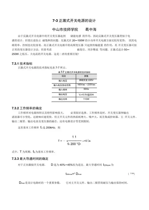
这是二者的重要区别!7.3.1技术指标正激式开关电源的技术指标见表7-7所示。
7.3.2工作频率的确定工作频率对电源体积以及特性影响很大,必须很好选择。
工作频率高时,开关变压器和输出滤波器可小型化,过渡响应速度快。
但主开关元件的热损耗增大、噪声大,而且集成控制器、主开关元件、输出二极管、输出电容及变压器的磁芯、还有电路设计等受到限制。
这里基本工作频率f o选200kHz,则1 1T = 一 = ---------- 3 =5(isf0 200 "O3式中,T为周期,f0为基本工作频率。
7.3.3最大导通时间的确定对于正向激励开关电源,D选为40%〜45%较为适宜。
最大导通时间t O N m ax为t oNmax=T D max ( 7-24)D max是设计电路时的一个重要参数,它对主开关元件、输出二极管的耐压与输出保持时间、变压器以及和输出滤波器的大小、转换效率等都有很大影响。
此处,选D max =45%。
由式(7-24),则有电压V O更小。
图7-26 “等积变形”示意图根据式(7-25),次级最低输出电压V2min为V2 minV O V L V F Tt oN max0.5 5=I4V 2.25式中,V F取0.5V (肖特基二极管),V L取0.3V。
2•变压器匝比的计算正激式开关电源中的开关变压器只起到传输能量|的作用,是真正意义上的变压器, 绕组的匝比N为V2根据交流输入电压的变动范围160V〜235V,则V I =200V〜350V, V|min=200V ,N =V|min= 200~ 14.3V2 min 14把式(7-25)、(7-25)整合,则变压器的匝比N为V im in D maxN =V O V L V F7.3.5变压器次级输出电压的计算变压器初级的匝数N!与最大工作磁通密度B m (高斯)之间的关系为max V|minB m S 104初、次级(7-26)所以有(7-27)(7-28)式中,S为磁芯的有效截面积(mm2), B m为最大工作磁通密度。