
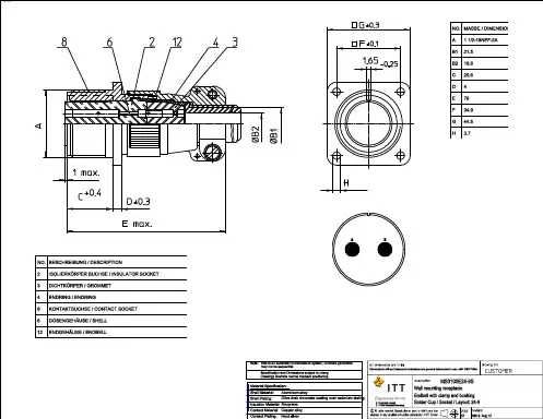
MS3100E24-9S;中文规格书,Datasheet资料
- 格式:pdf
- 大小:249.73 KB
- 文档页数:2

Timing Photo-Eye Kit,Adjustable Mount (75-33)The Adjustable Mount Timing Photo-Eye Kit is a pre-pack-aged and pre-wired electronic sensing and signalling assemblythat can be installed on a Dorner 2100 or 3100 Series Conveyor.Positions of both the Photo-Eye and Reflector can be adjustedvertically and laterally to improve the sensing of tall or elon-gated objects, as required. Use of the Timing Photo-Eye Kitallows selecting and presetting timed action and/or reactioncontrol delays.Figure 1: Photo-Eye Kit (75-33) InstalledE111–01Supply Voltage: 12-240 V olts DC (24-240 V olts AC), 2 WattsOutput Configuration: SPDT Relay OutputOutput Rating: 90 Watts (75 V olt-Amperes)Output Status: LED “ON” when Photo-Eye beam is blockedLight-emitting Element: Visible RedMaximum Sensing Distance: 15 ft (4.6 m)Detection Height Range: 1/2 to 7″ (13 to 178 mm)Above BeltHousing: Non Metallic, NEMA 6P/IP67Response Time: 20 millisecondsBCD ACovered under patent numbers 156,260 & 174,435 and corre-sponding patents and patent applications in other countries.Adjustable Mount Timing Photo-Eye Installation/Testing/Operation1.Verify all kit parts are present.Disconnect power to the Conveyor and to the impac Conveyor Controller. Due to the wide variety of setups & applications, guard-ing is the responsibility of the end user. NOTE:For shipping, the two Single Drop-in T-bars (D) and the Spacers (C) are pre-assembled to both the Photo-Eye (E) and Reflector (B) and mounting bracket assemblies with their respective fasteners. Detach the T-bars, Spacers and Refer to Figure 5 and attach Reflector with Mounting Bracket and Spacer to Single Drop-in T-bars using two M6 x 30 mm Socket Head Cap Screws. Tighten Screws with 5 mm Hex Key Wrench provided.CB ADFigure 7: Closure Strip Mounting Detail HE111–07aE111–07bd.To route Cable over a previously mounted component or to anchor the Cable, use the Zip Tie Mounts (G)and Single Drop-in T-bars (N), (Figure 8). Secure each Zip Tie Mount with an M6 x 10 mm Button Figure 8: Zip Tie Mounting DetailE111–08bFigure 9 shows a typical wire routing of a Photo-Eye anchor the extra Cable to the Zip Tie bel both ends of the Photo-Eye Cable using blank Labels (N) provided (Figure 10), using a permanent The Label should be wrapped around the Cable near the Photo-Eye and inside the impac Conveyor Controller to identify the Cable. When multiple Kits are used, make sure all Cables are uniquely labelled. (i.e., K1 for Kit #1,K2 for Kit #2,... etc.).NFigure 10: Cable Labeling (Detail providedonly on Photo-Eye End of Cable)Green Wire #3(T aped)Photo-EyeGreen #3Brown #4White #5Red #1Black #2Black RedGreenBrown White The C1 & C2 contacts are shown when the Photo-Eye Beam is blocked.C1C2Shown here is a sample application using a Photo-Eye to stop a normally running conveyor when a part blocks the Photo-Eye beam (Figure 12).When no part is present, the Photo-Eye contacts are closed which causes the conveyor to run.When a part is present, the Photo-Eye contacts are open which causes the conveyor to stop.Turn impac On/Off Switch to ON.The conveyor should run and the Photo-Eye’s status LED should be OFF.Dorner Mfg. Corp. reserves the right to change or discontinue products without notice. All products and。

DS31404 4-Input, 8-Output, Dual DPLL Timing ICwith Sub-ps Output JitterGeneral Description The DS31404 is a flexible, high-performance timing IC for diverse frequency conversion and frequency synthesis applications. On each of its four input clocks and eight output clocks, the device can accept or generate nearly any frequency between 2kHz and 750MHz. The device offers two independent DPLLs to serve two independent clock-generation paths.The input clocks are divided down, fractionally scaled as needed, and continuously monitored for activity and frequency accuracy. The best input clock is selected, manually or automatically, as the reference clock for each of the two flexible, high-performance digital PLLs. Each DPLL lock to the selected reference and provides programmable bandwidth, very high resolution holdover capability, and truly hitless switching between input clocks. The digital PLLs are followed by a clock synthesis subsystem that has four fully programmable digital frequency synthesis blocks, two high-speed low-jitter APLLs, and eight output clocks, each with its own 32-bit divider and phase adjustment. The APLLs provide fractional scaling and output jitter less than 1ps RMS. For telecom systems, the DS31404 has all required features and functions to serve as a central timing function or as a line card timing IC. With a suitable oscillator the DS31404 meets the requirements of Stratum 2, 3E, 3, 4E, and 4, G.812 Types I–IV, G.813, and G.8262.Applications Frequency Conversion Applications in a Wide Variety of Equipment TypesTelecom Line Cards or Timing Cards with Any Mix of SONET/SDH, Synchronous Ethernet and/or OTNPorts in WAN Equipment Including MSPPs, Ethernet Switches, Routers, DSLAMs, and Base StationsOrdering Information PART TEMP RANGE PIN-PACKAGE DS31404GN+ -40°C to +85°C 256 CSBGA+Denotes a lead(Pb)-free/RoHS-compliant package.SPI is a trademark of Motorola, Inc.Features ♦Four Input Clocks♦Differential or CMOS/TTL Format♦Any Frequency from 2kHz to 750MHz♦Fractional Scaling for 64B/66B and FECScaling (e.g., 64/66, 237/255, 238/255) or AnyOther Downscaling Requirement♦Continuous Input Clock Quality Monitoring♦Automatic or Manual Clock Selection♦Three 2/4/8kHz Frame Sync Inputs♦Two High-Performance DPLLs♦Hitless Reference Switching on Loss of Input♦Automatic or Manual Phase Build-Out♦Holdover on Loss of All Inputs♦Programmable Bandwidth, 0.5mHz to 400Hz♦Four Digital Frequency Synthesizers♦Each Can Slave to Either DPLL♦Produce Any 2kHz Multiple Up to 77.76MHz♦Per-DFS Clock Phase Adjust♦Two Output APLLs♦Output Frequencies to 750MHz♦High Resolution Fractional Scaling for FECand 64B/66B (e.g., 255/237, 255/238, 66/64)or Any Other Scaling Requirement♦Less than 1ps RMS Output Jitter♦Simultaneously Produce Two Low-Jitter Ratesfrom the Same Reference (e.g., 622.08MHzfor SONET and 156.25MHz for 10GE)♦Eight Output Clocks in Four Groups♦Nearly Any Frequency from < 1Hz to 750MHz♦Each Group Slaves to a DFS Clock, Any APLL Clock, or Any Input Clock (Divided and Scaled) ♦Each Has a Differential Output (2 CML, 2LVDS/LVPECL) and Separate CMOS/TTL Output ♦32-Bit Frequency Divider Per Output♦Two Sync Pulse Outputs: 8kHz and 2kHz♦General Features♦Suitable Line Card IC or Timing Card IC forStratum 2/3E/3/4E/4, SMC, SEC/EEC, or SSU ♦Accepts and Produces Nearly Any FrequencyUp to 750MHz Including 1Hz, 2kHz, 8kHz,NxDS1, NxE1, DS2/J2, DS3, E3, 2.5M, 25M,125M, 156.25M, and Nx19.44M Up to 622.08M ♦Internal Compensation for Local OscillatorFrequency Error♦SPI™ Processor Interface♦ 1.8V Operation with 3.3V I/O (5V Tolerant)Short Form Data Sheet April 2012Application ExampleBlock DiagramDetailed FeaturesInput Clock Features•Four input clocks, differential or CMOS/TTL signal format•Input clocks can be any frequency from 2kHz up to 750MHz•Supported telecom frequencies include PDH, SDH, Synchronous Ethernet, OTU-1, OTU-2, OTU-3 •Per-input fractional scaling (i.e., multiplying by N÷D where N is a 16-bit integer and D is a 32-bit integer and N < D) to undo 64B/66B and FEC scaling (e.g., 64/66, 238/255, 237/255, 236/255) •Special mode allows locking to 1Hz input clocks•All inputs constantly monitored by programmable activity monitors and frequency monitors•Fast activity monitor can disqualify the selected reference after a few missing clock cycles•Frequency measurement and frequency monitor thresholds with 0.2ppm resolution•Three optional 2/4/8kHz frame-sync inputsDPLL Features•Very high-resolution DPLL architecture•Sophisticated state machine automatically transitions between free-run, locked, and holdover states •Revertive or nonrevertive reference selection algorithm•Programmable bandwidth from 0.5mHz to 400Hz•Separately configurable acquisition bandwidth and locked bandwidth•Programmable damping factor to balance lock time with peaking: 1.2, 2.5, 5, 10 or 20•Multiple phase detectors: phase/frequency and multicycle•Phase/frequency locking (±360° capture) or nearest edge phase locking (±180° capture)•Multicycle phase detection and locking (up to ±8191UI) improves jitter tolerance and lock time•Phase build-out in response to reference switching for true hitless switching•Less than 1ns output clock phase transient during phase build-out•Output phase adjustment up to ±200ns in 6ps steps with respect to selected input reference•High-resolution frequency and phase measurement•Holdover frequency averaging over 1-second, 5.8-minute, and 93.2-minute intervals•Fast detection of input clock failure and transition to holdover mode•Low-jitter frame sync (8kHz) and multiframe sync (2kHz) aligned with output clocksDigital Frequency Synthesizer Features•Four independently programmable DFS blocks•Each DFS can slave to either of the DPLLs•Each DFS can synthesize any 2kHz multiple up to 77.76MHz•Per-DFS phase adjust (1/256UI steps)•Approximately 40ps RMS output jitterOutput APLL Features•Simultaneously produce two high-frequency, low-jitter, rates from the same reference clock, e.g., 622.08MHz for SONET and156.25MHz for 10GE•Standard telecom output frequencies include 622.08MHz, 155.52MHz, and 19.44MHz for SONET/SDH and 156.25MHz, 125MHz, and 25MHz for Synchronous Ethernet•Very high-resolution fractional scaling (i.e., noninteger multiplication)•Less than 1ps RMS output jitterOutput Clock Features•Eight output clock signals in four groups•Output clock groups OC1 and OC3 have a very high-speed differential output (current-mode logic, ≤ 750MHz) and a separate CMOS/TTL output (≤ 125MHz)•Output clock groups OC4 and OC5 have a high-speed differential output (LVDS/LVPECL, ≤ 312.5MHz) anda separate CMOS/TTL ouptut (≤ 125MHz)•Supported telecom frequencies include PDH, SDH, Synchronous Ethernet, OTU-1, OTU-2, OTU-3•Internal clock muxing allows each output group to slave to its associated DFS block, either of the APLLs, or any input clock (after being divided and scaled)•Outputs sourced directly from APLLs have less than 1ps RMS output jitter•Outputs sourced directly from DFS blocks have approximately 40ps RMS output jitter•Optional 32-bit frequency divider per output•8kHz frame sync and 2kHz multiframe sync outputs have programmable polarity and pulse width and can be disciplined by a 2kHz or 8kHz frame sync input•Per-output delay adjustment•Per-output enable/disable•All outputs disabled during resetGeneral Features•SPI serial microprocessor interface•Four general-purpose I/O pins•Register set can be write protected•Operates from a 12.8MHz, 25.6MHz, 10.24MHz, 20.48MHz, 10MHz, 20MHz, 19.44MHz, or 38.88MHz local oscillator•On-chip watchdog circuit for the local oscillator•Internal compensation for local oscillator frequency errorMicrosemi Corporate Headquarters One Enterprise, Aliso Viejo CA 92656 USA Within the USA: +1 (949) 380-6100 Sales: +1 (949) 380-6136Fax: +1 (949) 215-4996。