
31202D
- 格式:pdf
- 大小:410.02 KB
- 文档页数:11


用户手册PPC-3100/3120带 10.4”/12.1”彩色 TFT LCD 显示器和Intel® Atom处理器的微型计算机版权声明随附本产品发行的文件为研华公司2013年版权所有,并保留相关权利。
针对本手册中相关产品的说明,研华公司保留随时变更的权利,恕不另行通知。
未经研华公司书面许可,本手册所有内容不得通过任何途径以任何形式复制、翻印、翻译或者传输。
本手册以提供正确、可靠的信息为出发点。
但是研华公司对于本手册的使用结果,或者因使用本手册而导致其它第三方的权益受损,概不负责。
认可声明Intel和Pentium为Intel Corporation的商标。
Microsoft Windows®为Microsoft Corp.的注册商标。
所有其它产品名或商标均为各自所属方的财产。
PPC-3100/3120用户手册中文第一版,参照PPC-3100/3120用户手册英文第一版。
产品质量保证(两年)从购买之日起,研华为原购买商提供两年的产品质量保证。
但对那些未经授权的维修人员维修过的产品不予提供质量保证。
研华对于不正确的使用、灾难、错误安装产生的问题有免责权利。
如果研华产品出现故障,在质保期内我们提供免费维修或更换服务。
对于出保产品,我们将会酌情收取材料费、人工服务费用。
请联系相关销售人员了解详细情况。
如果您认为您购买的产品出现了故障,请遵循以下步骤:1.收集您所遇到的问题信息(例如,CPU主频、使用的研华产品及其它软件、硬件等)。
请注意屏幕上出现的任何不正常信息显示。
2.打电话给您的供货商,描述故障问题。
请借助手册、产品和任何有帮助的信息。
3.如果您的产品被诊断发生故障,请从您的供货商那里获得RMA (ReturnMaterial Authorization) 序列号。
这可以让我们尽快地进行故障产品的回收。
4.请仔细地包装故障产品,并在包装中附上完整的售后服务卡片和购买日期证明(如销售发票)。
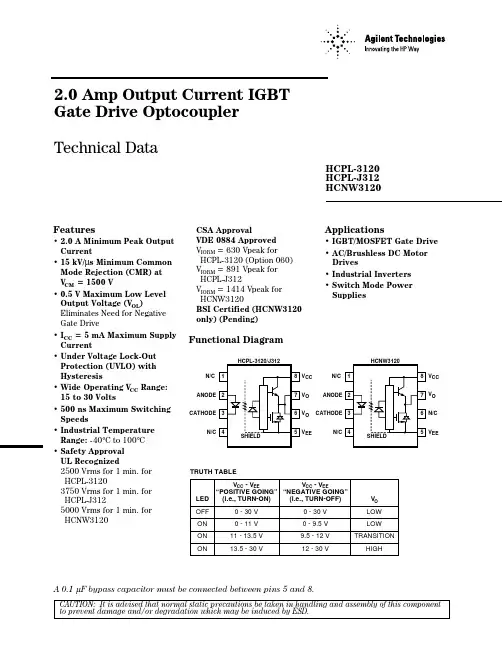
2.0 Amp Output Current IGBT Gate Drive Optocoupler Technical DataHCPL-3120HCPL-J312HCNW3120Features• 2.0 A Minimum Peak Output Current• 15 kV/µs Minimum Common Mode Rejection (CMR) at V CM = 1500 V• 0.5 V Maximum Low Level Output Voltage (V OL )Eliminates Need for Negative Gate Drive• I CC = 5 mA Maximum Supply Current• Under Voltage Lock-Out Protection (UVLO) with Hysteresis• Wide Operating V CC Range:15 to 30 Volts• 500 ns Maximum Switching Speeds• Industrial Temperature Range: -40°C to 100°C • Safety Approval UL Recognized2500 Vrms for 1 min. for HCPL-31203750 Vrms for 1 min. for HCPL-J3125000 Vrms for 1 min. for HCNW3120CSA ApprovalVDE 0884 Approved V IORM = 630 Vpeak for HCPL-3120 (Option 060)V IORM = 891 Vpeak for HCPL-J312V IORM = 1414 Vpeak for HCNW3120BSI Certified (HCNW3120only) (Pending)Applications• IGBT/MOSFET Gate Drive • AC/Brushless DC Motor Drives• Industrial Inverters • Switch Mode Power SuppliesA 0.1 µF bypass capacitor must be connected between pins 5 and 8.CAUTION: It is advised that normal static precautions be taken in handling and assembly of this componentto prevent damage and/or degradation which may be induced by ESD.Functional DiagramTRUTH TABLEV CC - V EE V CC - V EE“POSITIVE GOING”“NEGATIVE GOING”LED (i.e., TURN-ON)(i.e., TURN-OFF)V O OFF 0 - 30 V 0 - 30 V LOW ON 0 - 11 V 0 - 9.5 V LOW ON 11 - 13.5 V 9.5 - 12 V TRANSITIONON13.5 - 30 V12 - 30 VHIGH13SHIELD 248675N /CCATHODE ANODE N/C V CC V O V O V EE13SHIELD248675N /CCATHODE ANODE N/C V CC N/C V O V EEHCNW3120HCPL-3120/J312DescriptionThe HCPL-3120 contains a GaAsP LED while the HCPL-J312 and the HCNW3120 contain an AlGaAs LED. The LED is optically coupled to an integrated circuit with a power output stage. These optocouplers are ideally suited for driving power IGBTs and MOSFETs used in motor control inverter applications. The high operating voltage range of theoutput stage provides the drivevoltages required by gatecontrolled devices. The voltageand current supplied by theseoptocouplers make them ideallysuited for directly driving IGBTswith ratings up to 1200 V/100 A.For IGBTs with higher ratings,the HCPL-3120 series can beused to drive a discrete powerstage which drives the IGBT gate.The HCNW3120 has the highestinsulation voltage ofV IORM=1414Vpeak in theVDE0884. The HCPL-J312 has aninsulation voltage ofV IORM=891Vpeak and theV IORM=630Vpeak is alsoavailable with the HCPL-3120(Option060).Selection GuidePart Number HCPL-3120HCPL-J312HCNW3120HCPL-3150* Output Peak Current ( I O) 2.0 A 2.0 A 2.0 A0.5 AVDE0884 Approval V IORM=630 Vpeak V IORM=891 Vpeak V IORM=1414 Vpeak V IORM=630 Vpeak(Option 060)(Option 060)*The HCPL-3150 Data sheet available. Contact Agilent sales representative or authorized distributor.Ordering InformationSpecify Part Number followed by Option Number (if desired)Example:HCPL-3120#XXX060 = VDE0884, V IORM = 630 Vpeak (HCPL-3120 only)300 = Gull Wing Surface Mount Option500 = Tape and Reel Packaging OptionOption 500 contains 1000 units (HCPL-3120/J312), 750 units (HCNW3120) per reel.Other options contain 50 units (HCPL-3120/J312), 42 units (HCNW312) per tube.Option data sheets available. Contact Agilent sales representative or authorized distributor.(0.025 ± 0.005)MAX.(0.100)BSCDIMENSIONS IN MILLIMETERS (INCHES).LEAD COPLANARITY = 0.10 mm (0.004 INCHES).+ 0.076 - 0.051+ 0.003) - 0.002)Package Outline DrawingsHCPL-3120 and HCPL-J312 Outline Drawing (Standard DIP Package)HCPL-3120 and HCPL-J312 Gull Wing Surface Mount Option 300 Outline DrawingDIMENSIONS IN MILLIMETERS AND (INCHES).+ 0.076 - 0.051(0.010+ 0.003)- 0.002)* MARKING CODE LETTER FOR OPTION NUMBERS. "V" = OPTION 060OPTION NUMBERS 300 AND 500 NOT MARKED.1.78 ± 0.15 MAX.BSCDIMENSIONS IN MILLIMETERS (INCHES).LEAD COPLANARITY = 0.10 mm (0.004 INCHES).HCNW3120 Outline Drawing (8-Pin Wide Body Package)HCNW3120 Gull Wing Surface Mount Option 300 Outline Drawing1.78 ± 0.15 0.254+ 0.076 - 0.0051+ 0.003) - 0.002)Reflow Temperature ProfileRegulatory InformationAgency/StandardHCPL-3120HCPL-J312HCNW3120Underwriters Laboratory (UL)Recognized under UL 1577, Component RecognitionProgram, Category, File E55361Canadian Standards Association (CSA)File CA88324, per Component Acceptance Notice #5Verband Deutscher Electrotechniker (VDE)DIN VDE 0884 (June 1992)Option 060British Standards Institute (BSI)PendingCertification According to BS EN60065: 1994(BS415:1994), BS EN60950: 1992 (BS7002:1992)240TIME – MINUTEST E M P E R A T U R E – °C220200180160140120100806040200260MAXIMUM SOLDER REFLOW THERMAL PROFILE(NOTE: USE OF NON-CHLORINE ACTIVATED FLUXES IS RECOMMENDED.)Insulation and Safety Related SpecificationsValueHCPL-HCPL-HCNWParameter Symbol 3120J3123120Units ConditionsMinimum External L(101)7.17.49.6mmMeasured from input terminals to Air Gap (Clearance)output terminals, shortest distance through air.Minimum External L(102)7.48.010.0mmMeasured from input terminals to Tracking (Creepage)output terminals, shortest distance path along body.Minimum Internal 0.080.5 1.0mmInsulation thickness between emitter Plastic Gapand detector; also known as distance (Internal Clearance)through insulation.Tracking Resistance CTI >175>175>200VoltsDIN IEC 112/VDE 0303 Part 1(Comparative Tracking Index)Isolation GroupIIIa IIIa IIIaMaterial Group (DIN VDE 0110, 1/89,Table 1)VDE0884 Insulation Related CharacteristicsHCPL-3120DescriptionSymbolOption 060HCPL-J312HCNW3120UnitInstallation classification per DIN VDE 0110/1.89, Table 1for rated mains voltage ≤150 V rms I-IV I-IV I-IV for rated mains voltage ≤300 V rms I-IV I-IV I-IV for rated mains voltage ≤450 V rms I-IIII-III I-IV for rated mains voltage ≤600 V rms I-III I-IV for rated mains voltage ≤1000 V rms I-III Climatic Classification55/100/2155/100/2155/100/21Pollution Degree (DIN VDE 0110/1.89)222Maximum Working Insulation Voltage V IORM 6308911414V peak Input to Output Test Voltage, Method b*V PR118116702652V peakV IORM x 1.875 = V PR , 100% Production Test, t m = 1 sec, Partial Discharge < 5pC Input to Output Test Voltage, Method a*V PR 94513362121V peak V IORM x 1.5 = V PR , Type and SampleTest, t m = 60 sec, Partial Discharge < 5pC Highest Allowable Overvoltage*V IOTM600060008000V peak(Transient Overvoltage, t ini = 10 sec)Safety Limiting Values – maximum values allowed in the event of a failure,also see Figure 37. Case Temperature T S175175150°C Input Current I S INPUT 230400400mA Output PowerP S OUTPUT600600700mW Insulation Resistance at T S , V IO = 500 VR S≥109≥109≥109Ω*Refer to the VDE0884 section (page 1-6/8) of the Isolation Control Component Designer's Catalog for a detailed description of Method a/b partial discharge test profiles.Note: These optocouplers are suitable for “safe electrical isolation” only within the safety limit data. Maintenance of the safety data shall be ensured by means of protective circuits. Surface mount classification is Class A in accordance with CECC 00802.All Agilent data sheets report the creepage and clearance inherent to the optocoupler component itself. These dimensions areneeded as a starting point for the equipment designer whendetermining the circuit insulation requirements. However, once mounted on a printed circuit board, minimum creepage and clearance requirements must be met as specified for individual equipment standards. For creep-age, the shortest distance path along the surface of a printed circuit board between the solder fillets of the input and output leads must be considered. There are recommended techniques such as grooves and ribs which may be used on a printed circuit board to achieve desired creepage and clearances. Creepage and clearance distances will alsochange depending on factors such as pollution degree and insulation level.Absolute Maximum RatingsRecommended Operating ConditionsElectrical Specifications (DC)Over recommended operating conditions (T A = -40 to 100°C, I F(ON) = 7 to 16 mA, V F(OFF) = -3.0 to 0.8 V, V CC = 15 to 30 V, V EE = Ground) unless otherwise specified.*All typical values at T A = 25°C and V CC - V EE = 30 V, unless otherwise noted.Switching Specifications (AC)Over recommended operating conditions (T A = -40 to 100°C, I F(ON) = 7 to 16 mA, V F(OFF) = -3.0 to 0.8 V, V CC = 15 to 30 V, V EE = Ground) unless otherwise specified.*All typical values at T A = 25°C and V CC - V EE = 30 V, unless otherwise noted.Package CharacteristicsOver recommended temperature (T A = -40 to 100°C) unless otherwise specified.Parameter Symbol Device Min.Typ.Max.Units Test Conditions Fig.NoteInput-Output V ISO HCPL-31202500V RMS RH < 50%,8, 11Momentary HCPL-J3123750t = 1 min.,9, 11Withstand Voltage**HCNW31205000T A = 25°C 10, 11Resistance R I-O HCPL-31201012ΩV I-O = 500 V DC 11(Input-Output)HCPL-J312HCNW312010121013T A = 25°C1011T A = 100°CCapacitance C I-O HCPL-31200.6pF f = 1 MHz (Input-Output)HCPL-J3120.8HCNW31200.50.6LED-to-Case θLC 467°C/W Thermocouple 28Thermal Resistance LED-to-Detector θLD 442°C/W Thermal ResistanceDetector-to-Case θDC 126°C/W Thermal Resistance*All typicals at T A = 25°C.**The Input-Output Momentary Withstand Voltage is a dielectric voltage rating that should not be interpreted as an input-output continuous voltage rating. For the continuous voltage rating refer to your equipment level safety specification or Agilent Application Note 1074 entitled “Optocoupler Input-Output Endurance Voltage.”located at center underside ofpackage Notes:1. Derate linearly above 70°C free-air temperature at a rate of 0.3 mA/°C.2. Maximum pulse width = 10 µs,maximum duty cycle = 0.2%. This value is intended to allow forcomponent tolerances for designs with I O peak minimum = 2.0 A. See Applications section for additional details on limiting I OH peak.3. Derate linearly above 70°C free-air temperature at a rate of4.8 mW/°C.4. Derate linearly above 70°C free-air temperature at a rate of5.4 mW/°C.The maximum LED junction tempera-ture should not exceed 125°C.5. Maximum pulse width = 50 µs,maximum duty cycle = 0.5%.6. In this test V OH is measured with a dc load current. When driving capacitive loads V OH will approach V CC as I OH approaches zero amps.7. Maximum pulse width = 1 ms,maximum duty cycle = 20%.8. In accordance with UL1577, each optocoupler is proof tested by applying an insulation test voltage ≥3000 Vrms for 1 second (leakage detection current limit, I I-O ≤ 5 µA).9. In accordance with UL1577, each optocoupler is proof tested by applying an insulation test voltage ≥4500 Vrms for 1 second (leakage detection current limit, I I-O ≤ 5 µA).10. In accordance with UL1577, eachoptocoupler is proof tested by applying an insulation test voltage ≥6000 Vrms for 1 second (leakage detection current limit, I I-O ≤ 5 µA).11. Device considered a two-terminaldevice: pins 1, 2, 3, and 4 shorted together and pins 5, 6, 7, and 8shorted together.12. The difference between t PHL and t PLHbetween any two HCPL-3120 parts under the same test condition.13. Pins 1 and 4 need to be connected toLED common.14. Common mode transient immunity inthe high state is the maximum tolerable dV CM /dt of the common mode pulse, V CM , to assure that the output will remain in the high state (i.e., V O >15.0V).15. Common mode transient immunity ina low state is the maximum tolerable dV CM /dt of the common mode pulse,V CM , to assure that the output will remain in a low state (i.e., V O <1.0V).16. This load condition approximates thegate load of a 1200 V/75A IGBT.17. Pulse Width Distortion (PWD) isdefined as |t PHL -t PLH | for any given device.Figure 7. I CC vs. Temperature.Figure 8. I CC vs. V CC .Figure 4. V OL vs. Temperature.Figure 5. I OL vs. Temperature.Figure 6. V OL vs. I OL .Figure 1. V OH vs. Temperature.Figure 2. I OH vs. Temperature.Figure 3. V OH vs. I OH .(V O H – V C C ) – H I G H O U T P U T V O L T A G E D R O P – V-4T A – TEMPERATURE – °C -1-2-3I O H – O U T P U T HI G H C U R R E N T – AT A – TEMPERATURE – °C (V O H – V C C ) – O U T P U T H I G H V O L T A G E D R O P – VI OH – OUTPUT HIGH CURRENT – AV O L – O U T P U T L O W V O L T A G E – V0T A – TEMPERATURE – °C 0.250.050.150.200.10I O L – O U T P U T L O W C U R R E NT – AT A – TEMPERATURE – °CV O L – O U T P U T L O W V O L T A G E– VI OL – OUTPUT LOW CURRENT – A3412I C C – S U P P L Y C U R R E N T – m A1.5T A – TEMPERATURE – °C 3.02.53.52.0I C C – S U P P L Y C U R R E N T –m A1.5V CC – SUPPLY VOLTAGE – V3.02.53.52.0Figure 9. I FLH vs. Temperature.Figure 10. Propagation Delay vs. V CC .Figure 11. Propagation Delay vs. I F .Figure 12. Propagation Delay vs.Temperature.Figure 14. Propagation Delay vs. Cg.Figure 13. Propagation Delay vs. Rg.I F L H – L O W T O H I G H C U R R E N T T H R E S H O L D – m AT A – TEMPERATURE – °C 32415I F L H – L O W T O H I G H C U R R E N T T H R E S H O L D – m AT A – TEMPERATURE – °C HCPL-J312I F L H – L O W T O H I G H C U R R E N T T H R E S H O L D – m AT A – TEMPERATURE – °CHCNW3120T p – P R O P A G A T I O N D E L A Y – n s100V CC – SUPPLY VOLTAGE – V 400300500200T p – P R O P A G A T I O N D E L A Y – n s100I F – FORWARD LED CURRENT – mA 400300500200T p – P R O P A G A T I O N DE L A Y – n s100T A – TEMPERATURE – °C400300500200T p – P R O P A G A T I O N D E L A Y – n s100Rg – SERIES LOAD RESISTANCE – Ω400300500200T p – P R O P A G AT I O N D E L A Y – n s100Cg – LOAD CAPACITANCE – nF400300500200Figure 15. Transfer Characteristics.Figure 16. Input Current vs. Forward Voltage.Figure 17. I OH Test Circuit.V O – O U T P U T V O L T A G E – VI F – FORWARD LED CURRENT – mA5251513025342010HCPL-3120 / HCNW3120V O – O U T P U T V O L T A G E – V0I F – FORWARD LED CURRENT – mA1352551525341020HCPL-J31230I F – F O R W A R D C U R R E N T – m AV F – FORWARD VOLTAGE – VOLTSV F – FORWARD VOLTAGE – VOLTSI F – F O R W A R D C U R R E N T – m ACC = 15 to 30 VI F = 7 to 16 mAFigure 20. V OL Test Circuit.Figure 21. I FLH Test Circuit.Figure 19. V OH Test Circuit.Figure 18. I OL Test Circuit.Figure 22. UVLO Test Circuit.CC = 15 to 30 VCC = 15 to 30 VI F 16 mACC = 15 to 30 VCC = 15 to 30 VI FFigure 24. CMR Test Circuit and Waveforms.Figure 23. t PLH , t PHL , t r , and t f Test Circuit and Waveforms.CC = 15 to 30 V I= 30 VCM V OSWITCH AT B: I F = 0 mAV OSWITCH AT A: I F = 10 mA V OLV OHApplications InformationEliminating Negative IGBT Gate Drive (Discussion appliesto HCPL-3120, HCPL-J312, and HCNW3120)To keep the IGBT firmly off, the HCPL-3120 has a very low maximum V OL specification of 0.5V. The HCPL-3120 realizes this very low V OL by using a DMOS transistor with 1Ω(typical) on resistance in its pull down circuit. When the HCPL-3120 is in the low state, the IGBT gate is shorted to the emitter by Rg + 1Ω. Minimizing Rg and the lead inductance from the HCPL-3120 to the IGBT gate andemitter (possibly by mounting the HCPL-3120 on a small PC board directly above the IGBT) can eliminate the need for negative IGBT gate drive in many applica-tions as shown in Figure 25. Care should be taken with such a PC board design to avoid routing theIGBT collector or emitter traces close to the HCPL-3120 input as this can result in unwantedcoupling of transient signals into the HCPL-3120 and degrade performance. (If the IGBT drain must be routed near the HCPL-3120 input, then the LED should be reverse-biased when in the off state, to prevent the transient signals coupled from the IGBT drain from turning on the HCPL-3120.)Figure 25. Recommended LED Drive and Application Circuit.ACCONTROLINPUTSelecting the Gate Resistor (Rg) to Minimize IGBTSwitching Losses. (Discussion applies to HCPL-3120, HCPL-J312 and HCNW3120)Step 1: Calculate Rg Minimum from the I OL Peak Specifica-tion. The IGBT and Rg in Figure 26 can be analyzed as a simple RC circuit with a voltage supplied by the HCPL-3120.(V CC – V EE - V OL )Rg ≥–––––––––––––––I OLPEAK(V CC – V EE - 2 V )=–––––––––––––––I OLPEAK (15 V + 5 V - 2 V)=––––––––––––––––––2.5 A =7.2 Ω ≅ 8 ΩThe V OL value of 2V in the pre-vious equation is a conservative value of V OL at the peak current of 2.5A (see Figure 6). At lower Rg values the voltage supplied by the HCPL-3120 is not an ideal voltage step. This results in lower peak currents (more margin)than predicted by this analysis.When negative gate drive is not used V EE in the previous equation is equal to zero volts.Figure 26. HCPL-3120 Typical Application Circuit with Negative IGBT Gate Drive.AC- HVDCCONTROLINPUTStep 2: Check the HCPL-3120Power Dissipation and Increase Rg if Necessary. The HCPL-3120 total power dissipation (P T ) is equal to the sum of the emitter power (P E ) and the output power (P O ):P T = P E + P OP E = I F •V F •Duty CycleP O = P O(BIAS) + P O (SWITCHING)= I CC •(V CC - V EE )+ E SW (R G , Q G )•f For the circuit in Figure 26 with I F(worst case) = 16mA, Rg = 8Ω, Max Duty Cycle = 80%, Qg = 500 nC,f =20 kHz and T A max = 85C:P E = 16 mA •1.8 V •0.8 = 23 mW P O = 4.25 mA •20 V+ 5.2 µJ •20 kHz = 85 mW + 104 mW = 189 mW> 178 mW (P O(MAX) @ 85C = 250 mW −15C*4.8 mW/C)The value of 4.25 mA for I CC in the previous equation was obtained by derating the I CC max of 5 mA(which occurs at -40°C) to I CC max at 85C (see Figure 7).Since P O for this case is greater than P O(MAX), Rg must be increased to reduce the HCPL-3120 power dissipation.P O(SWITCHING MAX)= P O(MAX) - P O(BIAS)= 178 mW - 85 mW = 93 mWP O(SWITCHINGMAX)E SW(MAX)=–––––––––––––––f93 mW= ––––––– = 4.65 µW 20 kHzFor Qg = 500 nC, from Figure 27,a value of E SW = 4.65 µW gives a Rg = 10.3 Ω.P EParameterDescription I F LED Current V FLED On Voltage Duty CycleMaximum LED Duty CycleP O ParameterDescription I CC Supply Current V CC Positive Supply Voltage V EENegative Supply VoltageE SW (Rg,Qg)Energy Dissipated in the HCPL-3120 for eachIGBT Switching Cycle (See Figure 27)f Switching FrequencyFigure 27. Energy Dissipated in the HCPL-3120 for Each IGBT Switching Cycle.E s w – E N E R G Y P E R S W I T C H I N G C Y C L E – µJ0Rg – GATE RESISTANCE – Ω6144121082Thermal Model(Discussion applies to HCPL-3120, HCPL-J312and HCNW3120)The steady state thermal model for the HCPL-3120 is shown in Figure 28. The thermal resistance values given in this model can be used to calculate the tempera-tures at each node for a given operating condition. As shown by the model, all heat generated flows through θCA which raises the case temperature T Caccordingly. The value of θCAdepends on the conditions of the board design and is, therefore,determined by the designer. The value of θCA = 83°C/W wasobtained from thermal measure-ments using a 2.5 x 2.5 inch PCboard, with small traces (no ground plane), a single HCPL-3120 soldered into the center of the board and still air. The absolute maximum powerdissipation derating specifications assume a θCA value of 83°C/W.From the thermal mode in Figure 28 the LED and detector IC junction temperatures can be expressed as:T JE = P E • (θLC ||(θLD + θDC ) + θCA )θLC * θDC+ P D •(–––––––––––––––– + θCA )+ T AθLC + θDC + θLDθLC •θDCT JD = P E (––––––––––––––– + θCA)θLC + θDC + θLD+ P D •(θDC ||(θLD + θLC ) + θCA ) + T AInserting the values for θLC and θDC shown in Figure 28 gives:T JE = P E •(256°C/W + θCA ) + P D •(57°C/W + θCA ) + T A T JD = P E •(57°C/W + θCA )+ P D •(111°C/W + θCA ) + T A For example, given P E = 45 mW,P O = 250 mW, T A = 70°C and θCA = 83°C/W:T JE = P E •339°C/W + P D •140°C/W +T A= 45 mW •339°C/W + 250 m W•140°C/W + 70°C = 120°C T JD = P E •140°C/W + P D •194°C/W +T A= 45 mW •140C/W + 250 m W•194°C/W + 70°C = 125°CT JE and T JD should be limited to 125°C based on the board layout and part placement (θCA ) specific to the application.T JE =LED junction temperatureT JD =detector IC junction temperatureT C =case temperature measured at the center of the package bottom θLC =LED-to-case thermal resistance θLD =LED-to-detector thermal resistance θDC =detector-to-case thermal resistance θCA =case-to-ambient thermal resistance∗θCA will depend on the board design and the placement of the part.Figure 28. Thermal Model.θLD = 442 °C/W T JET JDθLC = 467 °C/WθDC = 126 °C/WθCA = 83 °C/W*T CT ALED Drive CircuitConsiderations for Ultra High CMR Performance.(Discussion applies to HCPL-3120, HCPL-J312, and HCNW3120)Without a detector shield, the dominant cause of optocoupler CMR failure is capacitivecoupling from the input side of the optocoupler, through the package, to the detector IC as shown in Figure 29. The HCPL-3120 improves CMR performanceby using a detector IC with an optically transparent Faraday shield, which diverts the capaci-tively coupled current away from the sensitive IC circuitry. How-ever, this shield does noteliminate the capacitive coupling between the LED and optocoup-ler pins 5-8 as shown in Figure 30. This capacitivecoupling causes perturbations in the LED current during common mode transients and becomes the major source of CMR failures forFigure 29. Optocoupler Input to OutputCapacitance Model for Unshielded Optocouplers.Figure 30. Optocoupler Input to OutputCapacitance Model for Shielded Optocouplers.a shielded optocoupler. The main design objective of a high CMR LED drive circuit becomes keeping the LED in the proper state (on or off) during common mode transients. For example,the recommended application circuit (Figure 25), can achieve 15kV/µs CMR while minimizing component complexity.Techniques to keep the LED in the proper state are discussed in the next two sections.CMR with the LED On (CMR H).A high CMR LED drive circuit must keep the LED on during common mode transients. This is achieved by overdriving the LED current beyond the input threshold so that it is not pulled below the threshold during a transient. A minimum LED cur-rent of 10 mA provides adequate margin over the maximum I FLH of 5mA to achieve 15kV/µs CMR.CMR with the LED Off(CMR L).A high CMR LED drive circuitmust keep the LED off (V F≤V F(OFF)) during common modetransients. For example, during a-dV cm/dt transient in Figure 31,the current flowing through C LEDPalso flows through the R SAT andV SAT of the logic gate. As long asthe low state voltage developedacross the logic gate is less thanV F(OFF), the LED will remain offand no common mode failure willoccur.The open collector drive circuit,shown in Figure 32, cannot keepthe LED off during a +dVcm/dttransient, since all the currentflowing through C LEDN must besupplied by the LED, and it is notrecommended for applicationsrequiring ultra high CMR Lperformance. Figure 33 is analternative drive circuit which,like the recommended applicationcircuit (Figure 25), does achieveultra high CMR performance byshunting the LED in the off state.CM • • •• • •Figure 33. Recommended LED Drive Circuit for Ultra-High CMR.Figure 31. Equivalent Circuit for Figure 25 During Common Mode Transient.Figure 32. Not Recommended Open Collector Drive Circuit.Under Voltage Lockout Feature. (Discussion applies toHCPL-3120, HCPL-J312, and HCNW3120)The HCPL-3120 contains an under voltage lockout (UVLO)feature that is designed to protect the IGBT under fault conditions which cause the HCPL-3120supply voltage (equivalent to thefully-charged IGBT gate voltage)to drop below a level necessary to keep the IGBT in a low resistance state. When the HCPL-3120output is in the high state and the supply voltage drops below the HCPL-3120 V UVLO– threshold (9.5<V UVLO– < 12.0) the opto-coupler output will go into the low state with a typical delay,UVLO Turn Off Delay, of 0.6µs.When the HCPL-3120 output is in the low state and the supply voltage rises above the HCPL-3120 V UVLO+ threshold (11.0 <V UVLO+ < 13.5) the optocoupler output will go into the high state (assumes LED is “ON”) with a typical delay, UVLO Turn On Delay of 0.8 µs.Figure 34. Under Voltage Lock Out.V O – O U T P U T V O L T A G E – V(V CC - V EE ) – SUPPLY VOLTAGE – V1014268412Figure 37. Thermal Derating Curve, Dependence of Safety Limiting Value with Case Temperature per VDE 0884.(DUE TO OPTOCOUPLER)= (t PHL MAX - t PHL MIN ) + (t PLH MAX - t PLH MIN ) = (t PHL MAX - t PLH MIN ) – (t PHL MIN - t PLH MAX ) = PDD* MAX – PDD* MIN*PDD = PROPAGATION DELAY DIFFERENCENOTE: FOR DEAD TIME AND PDD CALCULATIONS ALL PROPAGATIONDELAYS ARE TAKEN AT THE SAME TEMPERATURE AND TEST CONDITIONS.V OUT1I LED2V OUT2I LED1Figure 35. Minimum LED Skew for Zero Dead Time.Figure 36. Waveforms for Dead Time.*PDD = PROPAGATION DELAY DIFFERENCENOTE: FOR PDD CALCULATIONS THE PROPAGATION DELAYSARE TAKEN AT THE SAME TEMPERATURE AND TEST CONDITIONS.V OUT1I LED2V OUT2I LED1IPM Dead Time and Propagation DelaySpecifications. (Discussionapplies to HCPL-3120, HCPL-J312, and HCNW3120)The HCPL-3120 includes a Propagation Delay Difference (PDD) specification intended to help designers minimize “dead time” in their power inverterdesigns. Dead time is the time period during which both the high and low side powertransistors (Q1 and Q2 in Figure 25) are off. Any overlap in Q1and Q2 conduction will result in large currents flowing through the power devices between thehigh and low voltage motor rails.O U T P U T P O W E R – P S , I N P U T C U R R E N T – I S0T S – CASE TEMPERATURE – °C1000400600800200100300500700900O U T P U T P O W E R – P S , I N P U T C U R R E N T – I S0T S – CASE TEMPERATURE – °C 600400800200100300500700To minimize dead time in a given design, the turn on of LED2 should be delayed (relative to the turn off of LED1) so that under worst-case conditions, transistor Q1 has just turned off when transistor Q2 turns on, as shown in Figure 35. The amount of delay necessary to achieve this condi-tions is equal to the maximum value of the propagation delay difference specification, PDD MAX, which is specified to be 350ns over the operating temperature range of -40°C to 100°C.Delaying the LED signal by themaximum propagation delaydifference ensures that theminimum dead time is zero, but itdoes not tell a designer what themaximum dead time will be. Themaximum dead time is equivalentto the difference between themaximum and minimum propaga-tion delay difference specifica-tions as shown in Figure 36. Themaximum dead time for theHCPL-3120 is 700ns (= 350ns -(-350ns)) over an operatingtemperature range of -40°C to100°C.Note that the propagation delaysused to calculate PDD and deadtime are taken at equal tempera-tures and test conditions sincethe optocouplers under consider-ation are typically mounted inclose proximity to each other andare switching identical IGBTs.Data subject to change.Copyright © 1999 Agilent TechnologiesObsoletes 5965-4779E5965-7875E (11/99)。

XK3120C称重显示器/配料控制器使用说明书For personal use only in study and research; not for commercial useFor personal use only in study and research; not for commercial use一、主要技术指标及功能-----------------------------2二、For personal use only in study and research;not for commercial use三、四、面板及接口介绍-----------------------------------3五、安装流程说明--------------------------------------4六、校秤及配方设置操作说明-----------------------5七、For personal use only in study and research;not for commercial use八、九、参数设置信息详解--------------------------------6十、常用错误代码说明--------------------------------7 十一、注意事项--------------------------------------------9For personal use only in study and research; not for commercial useFor personal use only in study and research; not for commercial use郑州恒达电子有限公司地址:郑州市北环路19号For personal use only in study and research; not for commercial use 服务电话:,1,一、主要技术指标及功能1、主要功能◆6位LED数码主显示器, 2位LED数码副显示器◆3个LED工作状态指示灯◆具有模拟、数字双重滤波功能◆可实现自动、手动配料◆配料过程可随时暂停,重启后继续配料◆可实现配料启动前自动归零;上电、校秤前自动归零功能◆可控制1~6种不同种类的物料或1~3种粗精配物料◆可以预设10组配方信息功能,并可随意修改配方◆落差自动检测及保存、加锁功能◆校秤后可设置加锁、解锁功能◆一键式进入校秤状态、恢复出厂数据状态◆日期及时间设定、显示及打印功能(B型专用)◆具备手/自动打印功能◆数据设置错误或采集错误自动报警功能◆传感器数据非法或受干扰自动报警功能◆配料次数自动计数功能◆卸料方式可选择(单向卸料、双向卸料)◆具有RS-232通信接口◆具备打印机接口2、主要技术指标* 电源:交流220V或10V(-15%~+10%)50Hz(+2%)* 工作温度:-10°c~40°c* 相对湿度:<90%* 控制器功耗:<10W* 传感器类型:电阻应变式力传感器* 传感器供桥电压:DC5V* 称量量程:5KG~3000KG* 可配物料种类:1-6种* 采样速度:50~60次/秒* 非线性误差:<0.01%满度二、面板说明主显示面板如下图:1,主显示窗口:主要用于显示重量、配方、参数等信息。

OnCell3120-LTE-1SeriesIndustrial LTE Cat.1cellular gatewaysFeatures and Benefits•Low power consumption(40mW in standby)•GuaranLink for reliable cellular connectivity•Dual cellular operator backup with dual-SIM•Cellular WAN and Ethernet WAN backup mechanism for a complete pathredundancy•Rugged hardware design well suited for hazardous locations(ATEX Zone2/IECEx)•VPN secure connection capability with IPsec,GRE,and OpenVPN protocolsCertificationsIntroductionThe OnCell3120-LTE-1Series is a set of reliable,secure,low power consumption LTE gateways with state-of-the-art global LTE Cat1coverage. These LTE cellular gateways provide reliable connections from remote serial and Ethernet devices to a cellular network so that your applications can be easily implemented for IIoT remote-access scenarios.With its efficient power saving features,the OnCell3120-LTE-1Series lowers power consumption to less than40mW when in standby mode which can be managed using schedules.To enhance industrial reliability,the OnCell3120-LTE-1features GuaranLink to ensure robust cellular connectivity.Remote Access Gateway with VPN and Network Security•Managed by centralized IP management software,OnCell Central Manager•Secure and reliable VPN support with NAT/OpenVPN/GRE/IPsec functionality•Cybersecurity features based on IEC62443-4-2Industrial-grade Reliability•Rugged hardware design well suited for hazardous locations(ATEX,C1D2,IECEx)•GuaranLink for reliable cellular connectivity•WAN backup between cellular and Ethernet•-30to70°C wide operating temperature•Low power consumption:Less than40mW in standby modeSpecificationsCellular InterfaceCellular Standards LTE CAT-1,HSPA,UMTS,EDGE,GPRS,GSMLTE Data Rate10MHz bandwidth:10.2Mbps DL,5.2Mbps ULHSPA Data Rates7.2Mbps DL,5.76Mbps ULBand Options(EU)LTE Band1(2100MHz)/LTE Band3(1800MHz)/LTE Band7(2600MHz)/LTE Band8(900MHz)/LTE Band20(800MHz)/LTE Band28A(700MHz)UMTS/HSPA900MHz/1800MHz/2100MHzGSM900MHz/1800MHzBand Options(AU)LTE Band3(1800MHz)/LTE Band5(850MHz)/LTE Band8(900MHz)/LTE Band28(700MHz)UMTS/HSPA2100MHz/850MHz/900MHzBand Options(US)LTE Band2(1900MHz)/LTE Band4(1700MHz(AWS))/LTE Band5(850MHz)/LTEBand12(700MHz)/LTE Band13(700MHz)/LTE Band14(700MHz)/LTE Band66(1700MHz)/LTE Band71(600MHz)UMTS/HSPA1900MHz/1700MHz/850MHzNo.of SIMs2SIM Format Nano SIMCellular Antenna Connectors2SMA femaleEthernet Interface10/100BaseT(X)Ports(RJ45connector)2USB InterfaceNo.of USB Ports1USB Connector USB Type AUSB Standards USB2.0Serial InterfaceNo.of Ports1Connector DB9maleSerial Standards RS-232/422/485Data Bits5,6,7,8Stop Bits1,1.5,2Parity None,Even,Odd,Space,MarkBaudrate75bps to921.6kbpsConsole Port RS-232(TxD,RxD,GND),4-pin header output(115200,n,8,1)Serial SignalsRS-232TxD,RxD,RTS,CTS,DTR,DSR,DCD,GNDRS-422Tx+,Tx-,Rx+,Rx-,GNDRS-485-2w Data+,Data-,GNDRS-485-4w Tx+,Tx-,Rx+,Rx-,GNDEthernet Software FeaturesManagement GuaranLink,DHCP server,DDNS,ARP,Telnet,TCP/IP,UDP,SMTP,Remote SMSControl,Power Saving,Syslog,SNMPv1/v2c/v3,Serial Console,Telnet Console,WebConsole,OnCell Central Manager,Wireless Search UtilityFirewall Filter:MAC,IP protocol,port-based,Access IP listSecurity HTTPSTime Management SNTP ClientIPsec VPNAuthentication PSK/X.509/RSAEncryption DES,3DES,AES,MD5,SHA-1,DH2,DH5Concurrent VPN Tunnels5NATFeatures NAT loopback,1-to-1,N-to-1,Port forwardingOpenVPNOpenVPN OpenVPN(client and server),Tunnel mode(routing)and TAP mode(bridge) Encryption Blowfish CBC,DES CBC,DES-EDE3CBC,AES-128/192/256CBC Concurrent VPN Tunnels5Power ParametersInput Current0.8A(max.)Input Voltage9to36VDCPower Consumption5W(typ.)Power Connector Terminal blockReverse Polarity Protection SupportedPower Button Reset buttonPhysical CharacteristicsHousing MetalIP Rating IP30Dimensions128.5x26x89.1mm(5.06x1.02x3.51in)Weight550g(1.22lb)Installation DIN-rail mounting,Wall mounting(with optional kit)Environmental LimitsOperating Temperature Standard Models:0to55°C(32to131°F)Wide Temp.Models:-30to70°C(-22to158°F)Storage Temperature(package included)-40to85°C(-40to185°F)Ambient Relative Humidity5to95%(non-condensing)Standards and CertificationsEMC EN55032/35,EN61000-6-2/-6-4EMI CISPR22,FCC Part15B Class AEMS IEC61000-4-2ESD:Contact:4kV;Air:8kVIEC61000-4-3RS:80MHz to1GHz:10V/mIEC61000-4-4EFT:Power:1kV;Signal:1kVIEC61000-4-5Surge:Power:1kV;Signal:1kVIEC61000-4-6CS:10V;150kHz to80MHzIEC61000-4-8:30A/mFreefall IEC60068-2-32Hazardous Locations ATEX,IECEx,Class I Division2Radio Frequency PTCRB,FCC ID SLE-LE910CXNFRadio RCM,KCCarrier Approvals VerizonAT&TCellular Standards EN301511EN301908-1EN62311(MPE SAR)AS/CA S042EN301489-1/-52Safety IEC60950-1,IEC62368-1,UL60950-1,UL62368-1 Shock IEC60068-2-27Vibration IEC60068-2-6Green Product RoHS,CRoHS,WEEEMTBFTime585,775hrsStandards Telcordia SR332WarrantyWarranty Period5yearsDetails See /warrantyPackage ContentsDevice1x OnCell3120-LTE-1Series LTE cellular gateway1 Installation Kit1x DIN-rail kitDocumentation1x quick installation guide1x warranty cardDimensions1.An activated nano SIM card(not included)must be provided by a third party Cellular Service Provider.Ordering InformationOnCell3120-LTE-1-EU LTE Cat1B1(2100MHz)/B3(1800MHz)/B7(2600MHz)/B8(900MHz)/B20(800MHz)/B28A(700MHz)-0to55°C Wall,DIN railOnCell3120-LTE-1-EU-T LTE Cat1B1(2100MHz)/B3(1800MHz)/B7(2600MHz)/B8(900MHz)/B20(800MHz)/B28A(700MHz)-30to70°C Wall,DIN railOnCell3120-LTE-1-AU LTE Cat1B3(1800MHz)/B5(850MHz)/B8(900MHz)/B28(700MHz)-0to55°C Wall,DIN railOnCell3120-LTE-1-AU-T LTE Cat1B3(1800MHz)/B5(850MHz)/B8(900MHz)/B28(700MHz)-30to70°C Wall,DIN railOnCell3120-LTE-1-US LTE Cat1B2(1900MHz)/B4(1700MHz)/B5(850MHz)/B12(700MHz)/B13(700MHz)/B14(700MHz)/B66(1700MHz)/B71(600MHz)-0to55°C Wall,DIN railOnCell3120-LTE-1-US-T LTE Cat1B2(1900MHz)/B4(1700MHz)/B5(850MHz)/B12(700MHz)/B13(700MHz)/B14(700MHz)/B66(1700MHz)/B71(600MHz)-30to70°C Wall,DIN railAccessories(sold separately)AntennasANT-LTEUS-ASM-01GSM/GPRS/EDGE/UMTS/HSPA/LTE,omni-directional rubber duck antenna,1dBiANT-LTE-ASM-02GPRS/EDGE/UMTS/HSPA/LTE,omni-directional rubber duck antenna,2dBiANT-LTE-ANF-04GSM/GPRS/EDGE/UMTS/HSPA/LTE,omni-directional outdoor antenna,4dBi,IP66Wireless Antenna CablesCRF-SMA(M)/N(M)-300N-type(male)to SMA(male)CFD200cable,3mA-CRF-SMSF-R3-100Cellular magnetic base,SMA connector,1mMounting KitsWK-35-042plates(35x44x2.5mm)with6screws(FTSx6M3x4mm)©Moxa Inc.All rights reserved.Updated May04,2022.This document and any portion thereof may not be reproduced or used in any manner whatsoever without the express written permission of Moxa Inc.Product specifications subject to change without notice.Visit our website for the most up-to-date product information.。