RT9013-32PB中文资料
- 格式:pdf
- 大小:309.59 KB
- 文档页数:12
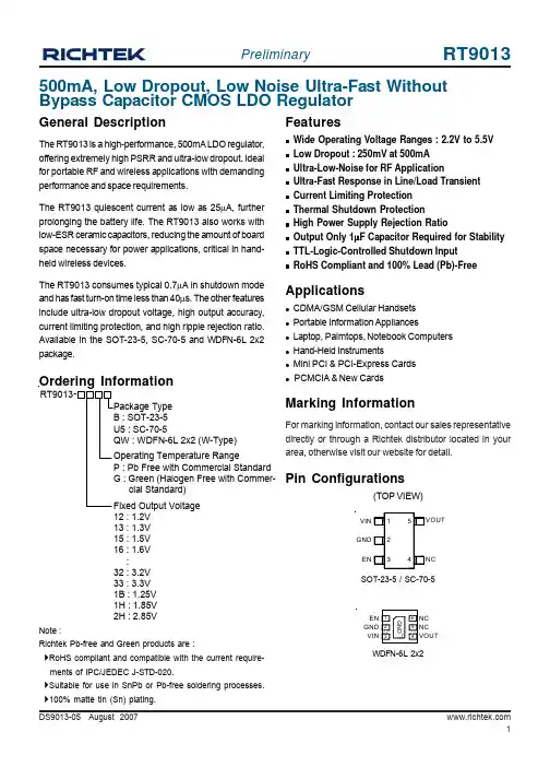
1DS9013-05 August 2007Pin ConfigurationsApplicationsCDMA/GSM Cellular Handsets Portable Information AppliancesLaptop, Palmtops, Notebook Computers Hand-Held InstrumentsMini PCI & PCI-Express Cards PCMCIA & New Cards500mA, Low Dropout, Low Noise Ultra-Fast Without Bypass Capacitor CMOS LDO RegulatorOrdering InformationMarking InformationFor marking information, contact our sales representative directly or through a Richtek distributor located in your area, otherwise visit our website for detail.General DescriptionThe RT9013 is a high-performance, 500mA LDO regulator,offering extremely high PSRR and ultra-low dropout. Ideal for portable RF and wireless applications with demanding performance and space requirements.The RT9013 quiescent current as low as 25μA, further prolonging the battery life. The RT9013 also works with low-ESR ceramic capacitors, reducing the amount of board space necessary for power applications, critical in hand-held wireless devices.The RT9013 consumes typical 0.7μA in shutdown mode and has fast turn-on time less than 40μs. The other features include ultra-low dropout voltage, high output accuracy,current limiting protection, and high ripple rejection ratio.Available in the SOT-23-5, SC-70-5 and WDFN-6L 2x2package.(TOP VIEW)WDFN-6L 2x2FeaturesWide Operating Voltage Ranges : 2.2V to 5.5V Low Dropout : 250mV at 500mA Ultra-Low-Noise for RF ApplicationUltra-Fast Response in Line/Load Transient Current Limiting Protection Thermal Shutdown ProtectionHigh Power Supply Rejection RatioOutput Only 1μF Capacitor Required for Stability TTL-Logic-Controlled Shutdown InputRoHS Compliant and 100% Lead (Pb)-FreeSOT-23-5 / SC-70-5RT901312 : 1.2V 13 : 1.3V 15 : 1.5V 16 : 1.6V :32 : 3.2V 33 : 3.3V 1B : 1.25V 1H : 1.85V 2H : 2.85VNote :Richtek Pb-free and Green products are :`RoHS compliant and compatible with the current require- ments of IPC/JEDEC J-STD-020.`Suitable for use in SnPb or Pb-free soldering processes.`100% matte tin (Sn) plating.EN GND NC NC VOUTVINGND VIN EN2DS9013-05 August 2007 Typical Application CircuitFunctional Pin DescriptionFunction Block DiagramV OUTENVINAbsolute Maximum Ratings (Note 1)Supply Input Voltage------------------------------------------------------------------------------------------------------6VEN Input Voltage-----------------------------------------------------------------------------------------------------------6VPower Dissipation, P D @ T A= 25°CSOT-23-5--------------------------------------------------------------------------------------------------------------------0.4WSC-70-5----------------------------------------------------------------------------------------------------------------------0.3WWDFN-6L 2x2--------------------------------------------------------------------------------------------------------------0.606WPackage Thermal Resistance (Note 4)SOT-23-5, θJA---------------------------------------------------------------------------------------------------------------250°C/WSC-70-5, θJA----------------------------------------------------------------------------------------------------------------333°C/W WDFN-6L 2x2, θJA---------------------------------------------------------------------------------------------------------165°C/W WDFN-6L 2x2, θJC---------------------------------------------------------------------------------------------------------20°C/WLead Temperature (Soldering, 10 sec.)-------------------------------------------------------------------------------260°CJunction T emperature-----------------------------------------------------------------------------------------------------125°CStorage T emperature Range--------------------------------------------------------------------------------------------−65°C to 150°C ESD Susceptibility (Note 2)HBM--------------------------------------------------------------------------------------------------------------------------2kVMM----------------------------------------------------------------------------------------------------------------------------200V Recommended Operating Conditions (Note 3)Supply Input Voltage------------------------------------------------------------------------------------------------------2.2V to 5.5VJunction T emperature Range--------------------------------------------------------------------------------------------−40°C to 125°C Ambient T emperature Range--------------------------------------------------------------------------------------------−40°C to 85°C Electrical Characteristics(V= V + 0.5V, V= V, C= C= 1μF (Ceramic), T= 25°C unless otherwise specified)To be continuedDS9013-05 August 34DS9013-05 August 2007 Note 1. Stresses listed as the above “Absolute Maximum Ratings ” may cause permanent damage to the device. These are forstress ratings. Functional operation of the device at these or any other conditions beyond those indicated in the operational sections of the specifications is not implied. Exposure to absolute maximum rating conditions for extended periods may remain possibility to affect device reliability.Note 2. Devices are ESD sensitive. Handling precaution recommended.Note 3. The device is not guaranteed to function outside its operating conditions.Note 4. θJA is measured in the natural convection at T A = 25°C on a low effective thermal conductivity test board of JEDEC 51-3thermal measurement standard. The case position of θJC is on the exposed pad for the WDFN-6L 2x2 packages.Note 5. Quiescent, or ground current, is the difference between input and output currents. It is defined by I Q = I IN - I OUT under noload condition (I OUT = 0mA). The total current drawn from the supply is the sum of the load current plus the ground pin current.Note 6. The dropout voltage is defined as V IN -V OUT , which is measured when V OUT is V OUT(NORMAL) - 100mV.Note 7. Regulation is measured at constant junction temperature by using a 2ms current pulse. Devices are tested for loadregulation in the load range from 10mA to 500mA.5DS9013-05 August 2007Typical Operating CharacteristicsOutput Voltage vs. Temperature1.401.421.441.461.481.501.521.541.561.581.60-50-25255075100125Temperature O u t p u t V o l t a g e (V )(°C)(C IN = C OUT = 1μ/X7R, unless otherwise specified)Dropout Voltage vs. Load Current050100150200250300350050100150200250300350400450500Load Current (mA)D r o p o u t V o l t a ge (m V )V IN = 2.5V, I LOAD = 75mA Start UpTime (5μs/Div)E N P i n V o l t a g e (V )O u t p u t V o l t a g e (V )4201.00.50RT9013-15PQWV IN = 2.5V, I LOAD = 50mA EN Pin Shutdown ResponseE N P i n V o l t a g e (V )Time (100μs/Div)O u t p u t V o l t a g e (V )420210RT9013-15PQW Quiescent Current vs. Temperature1012141618202224262830-50-250255075100125Temperature Q u i e s c e n t C u r r e n t (u A )(°C)Dropout Voltage vs. Load Current50100150200250300350050100150200250300350400450500Load Current (mA)D r o p o u t V o l t a g e (m V )6DS9013-05 August 2007 V IN = 2.5V, I LOAD= 10mA to 100mAL o a d C u r r e n t (m A )Time (100μs/Div)O u t p u t V o l t a g e D e v i a t i o n (m V )100500500-50RT9013-15PQWV IN = 2.5V, I LOAD = 10mA to 300mAL o a d C u r r e n t (m A )Time (100μs/Div)O u t p u t V o l t a g e D e v i a t i o n (m V )4002000500-50RT9013-15PQWV IN = 2.6V to 3.6V, I LOAD = 10mAI n p u t V o l t ag e D e v i a t i o n (V )Time (100μs/Div)O u t p u t V o l t a g e D e v i a t i o n (m V )3.62.6200-20RT9013-15PQWI n p u t V o l t a g e De v i a t i o n (V )Time (100μs/Div)O u t p u t V o l t a g e D e v i at i o n (m V )3.62.6200-20V IN = 2.6V to 3.6V, I LOAD = 100mART9013-15PQWTime (10ms/Div)V IN = 3.0V (By Battery), No Load NoiseTime (10ms/Div)N o i s e (μV /D i v )3002001000-100-200-300RT9013-15PQW7DS9013-05 August 2007PSRR-70-60-50-40-30-20-1001020101001000100001000001000000Frequency (Hz)P S R R (d B )Time (10ms/Div)8DS9013-05 August 2007 Applications InformationLike any low-dropout regulator, the external capacitors used with the RT9013 must be carefully selected for regulator stability and performance. Using a capacitor whose value is > 1μF on the RT9013 input and the amount of capacitance can be increased without limit. The input capacitor must be located a distance of not more than 0.5 inch from the input pin of the IC and returned to a clean analog ground.Any good quality ceramic can be used for this capacitor.The capacitor with larger value and lower ESR (equivalent series resistance) provides better PSRR and line-transient response.The output capacitor must meet both requirements for minimum amount of capacitance and ESR in all LDOs application. The RT9013 is designed specifically to work with low ESR ceramic output capacitor in space-saving and performance consideration. Using a ceramic capacitor whose value is at least 1μF with ESR is > 20m Ω on the RT9013 output ensures stability. The RT9013 still works well with output capacitor of other types due to the wide stable ESR range. Figure 1. shows the curves of allowable ESR range as a function of load current for various output capacitor values. Output capacitor of larger capacitance can reduce noise and improve load transient response,stability, and PSRR. The output capacitor should be located not more than 0.5 inch from the VOUT pin of the RT9013and returned to a clean analog ground.Figure 1EnableThe RT9013 goes into sleep mode when the EN pin is in a logic low condition. During this condit ion, the RT9013 has an EN pin to turn on or turn off regulator, When the EN pin is logic hight, the regulator will be turned on. The supply current to 0.7μA typical. The EN pin may be directly tied to V IN to keep the part on. The Enable input is CMOS logic and cannot be left floating.PSRRThe power supply rejection ratio (PSRR) is defined as the gain from the input to output divided by the gain from the supply to the output. The PSRR is found to be⎟⎠⎞⎜⎝⎛×=ΔSupply Error ΔGain log 20 PSRR Note that when heavy load measuring, Δsupply will cause Δtemperature. And Δtemperature will cause Δoutput voltage. So the heavy load PSRR measuring is include temperature effect.Current limitThe RT9013 contains an independent current limiter, which monitors and controls the pass transistor's gate voltage,limiting the output current to 0.6A (typ.). The output can be shorted to ground indefinitely without damaging the part.Thermal ConsiderationsThermal protection limits power dissipation in RT9013.When the operation junction temperature exceeds 170°C,the OTP circuit starts the thermal shutdown function and turns the pass element off. The pass element turn on again after the junction temperature cools by 30°C.For continuous operation, do not exceed absolute maximum operation junction temperature 125°C. The power dissipation definition in device is :P D = (V IN − V OUT ) x I OUT + V IN x I QThe maximum power dissipation depends on the thermal resistance of IC package, PCB layout, the rate of surroundings airflow and temperature difference between junction to ambient. The maximum power dissipation can be calculated by following formula :P D(MAX) = ( T J(MAX) − T A ) /θJARegion of Stable C OUT ESR vs. Load Current0.0010.010.1110100100200300400500Load Current (mA)R e g i o n o f S t a b l e C O U T E S R (Ω)9DS9013-05 August 2007Figure 2. Derating Curves for RT9013 PackagesWhere T J(MAX) is the maximum operation junction temperature, T A is the ambient temperature and the θJA is the junction to ambient thermal resistance.For recommended operating conditions specification of RT9013, where T J(MAX) is the maximum junction temperature of the die (125°C) and T A is the operated ambient temperature. The junction to ambient thermal resistance θJA (θJA is layout dependent) for WDFN-6L 2x2package is 165°C/W, SOT-23-5 package is 250°C/W and SC-70-5 package is 333°C/W on the standard JEDEC 51-3 single-layer thermal test board. The maximum power dissipation at T A = 25°C can be calculated by following formula :P D(MAX) = (125°C − 25°C) / 165 = 0.606 W for WDFN-6L 2x2 packagesP D(MAX) = (125°C − 25°C) / 250 = 0.400 W for SOT-23-5packagesP D(MAX) = (125°C − 25°C) / 333 = 0.300 W for SC-70-5packagesThe maximum power dissipation depends on operating ambient temperature for fixed T J(MAX) and thermal resistance θJA . For RT9013 packages, the Figure 2 of derating curves allows the designer to see the effect of rising ambient temperature on the maximum power allowed.00.10.20.30.40.50.60.7012.52537.55062.57587.5100113125Ambient Temperature P o w e r D is s i p a t i o n (W )(°C)10DS9013-05 August 2007Outline DimensionA1HLSOT-23-5 Surface Mount PackageRT9013Preliminary11DS9013-05 August 2007A1HLSC -70-5 Surface Mount Package12DS9013-05 August 2007Richtek Technology CorporationHeadquarter5F, No. 20, Taiyuen Street, Chupei City Hsinchu, Taiwan, R.O.C.Tel: (8863)5526789 Fax: (8863)5526611Richtek Technology CorporationTaipei Office (Marketing)8F, No. 137, Lane 235, Paochiao Road, Hsintien City Taipei County, Taiwan, R.O.C.Tel: (8862)89191466 Fax: (8862)89191465Email: marketing@W-Type 6L DFN 2x2 Package。