半导体工艺学silvaco仿真实验报告
- 格式:pdf
- 大小:2.25 MB
- 文档页数:46
4.1.7栅氧厚度的最优化下面介绍如何使用DECKBUILD中的最优化函数来对栅极氧化厚度进行最优化。
假定所测量的栅氧厚度为100Å,栅极氧化过程中的扩散温度和偏压均需要进行调整。
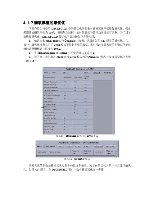
为了对参数进行最优化,DECKBUILD最优化函数应按如下方法使用:a.依次点击Main control和Optimizer…选项;调用出如图4.15所示的最优化工具。
第一个最优化视窗显示了Setup模式下控制参数的表格。
我们只改变最大误差参数以便能精确地调整栅极氧化厚度为100Å;b.将Maximum Error在criteria一栏中的值从5改为1;c.接下来,我们通过Mode键将Setup模式改为Parameter模式,并定义需要优化参数(图4.16)。
图4.15 DECKBUILD最优化的Setup模式图4.16 Parameter模式需要优化的参数是栅极氧化过程中的温度和偏压。
为了在最优化工具中对其进行最优化,如图4.17所示,在DECKBUILD窗口中选中栅极氧化这一步骤;图4.17 选择栅极氧化步骤d.然后,在Optimizer中,依次点击Edit和Add菜单项。
一个名为Deckbuild:Parameter Define的窗口将会弹出,如图4.18所示,列出了所有可能作为参数的项;图4.18 定义需要优化的参数e.选中temp=<variable>和press=<variable>这两项。
然后,点击Apply。
添加的最优化参数将如图4.19所示一样列出;图4.19 增加的最优化参数f.接下来,通过Mode键将Parameter模式改为Targets模式,并定义优化目标;g.Optimizer利用DECKBUILD中Extract语句的值来定义优化目标。
因此,返回DECKBUILD的文本窗口并选中Extract栅极氧化厚度语句,如图4.20所示;图4.20 选中优化目标h.然后,在Optimizer中,依次点击Edit和Add项。
Indium Implant and Anneal1 go athena23 #TITLE: Indium Anneal45 #the x dimension definition6 line x loc = 0.0 spacing=0.17 line x loc = 0.1 spacing=0.189 #the vertical definition10 line y loc = 0 spacing = 0.0211 line y loc = 2.0 spacing = 0.201213 #initialize the mesh14 init silicon c.phos=1.0e141516 #perform uniform boron implant17 implant indium dose=1e13 energy=70 monte18 structure outfile=andfex12_0.str1920 #perform diffusion21 diffuse time=30 temperature=1000222324 extract name="xj" xj silicon mat.occno=1 x.val=0.0 junc.occno=12526 #save the structure27 structure outfile=andfex12_1.str2829 tonyplot -overlay andfex12_0.str andfex12_1.str -set andfex12.set3031 quitOxidation Enhanced Diffusion of Boron1 go athena23 # OED of Boron45 #the x dimension definition6 line x loc = 0.0 spacing=0.17 line x loc = 0.1 spacing=0.189 #the vertical definition10 line y loc = 0 spacing = 0.0211 line y loc = 2.0 spacing = 0.2012 line y loc = 25.0 spacing = 2.51314 #initialize the mesh15 init silicon c.boron=1.0e141617 #perform uniform boron implant18 implant boron dose=1e13 energy=701920 #set diffusion model for OED21 method two.dim2223 #perform diffusion24 diffuse time=30 temperature=1000 dryo225 #26 extract name="xj_two.dim" xj silicon mat.occno=1 x.val=0.0 junc.occno=12728 #save the structure29 structure outfile=andfex02_0.str3031 # repeat the simulation with default FERMI model32 go athena3334 #TITLE: Simple Boron Anneal3536 #the x dimension definition37 line x loc = 0.0 spacing=0.138 line x loc = 0.1 spacing=0.13940 #the vertical definition41 line y loc = 0 spacing = 0.0242 line y loc = 2.0 spacing = 0.2043 line y loc = 25.0 spacing = 2.54445 #initialize the mesh46 init silicon c.phos=1.0e144748 #perform uniform boron implant49 implant boron dose=1e13 energy=705051 #select diffusion model52 method fermi5354 #perform diffusion55 diffuse time=30 temperature=1000 dryo256 #57 extract name="xj_fermi" xj silicon mat.occno=1 x.val=0.0 junc.occno=1585960 #save the structure61 structure outfile=andfex02_1.str6263 # compare diffusion models64 tonyplot -overlay andfex02_0.str andfex02_1.str -set andfex02.set Emitter Push Effect1 go athena23 #TITLE: Emitter push effect example4 #5 line x loc=0.0 spac=0.26 line x loc=2.5 spac=0.87 line x loc=3.0 spac=0.28 #9 line y loc=0.00 spac=0.0410 line y loc=0.3 spac=0.0611 line y loc=2.0 spac=0.812 line y loc=10.0 spac=2.013 #14 init c.phos=1e1515 #16 implant boron dose=1e13 energy=4017 #18 deposit nitride thick=.2 div=419 #20 etch right nitride p1.x=2.521 relax y.min=1.522 #23 implant phosphor dose=1e16 energy=3024 #25 etch nitride all26 #27 method compress full.cpl28 diffuse time=30 temp=100029 #30 structure outfile=andfex07.str31 #32 tonyplot -st andfex07.str -set andfex07.set3334 quitDamage Enhanced Diffusion of ArsenicThis example demonstrates the damage enhanced diffusion effect in a heavy arsenic implant typical of MOS source/drain or bipolar emitter processing.1 go athena23 #the x dimension definition4 line x loc = 0.0 spacing=0.15 line x loc = 0.1 spacing=0.167 #the vertical definition8 line y loc = 0 spacing = 0.0059 line y loc = 2.0 spacing = 0.2010 line y loc = 25.0 spacing = 2.51112 #initialize the mesh13 init silicon c.boron=1.0e171415 #deposit screen oxide16 deposit oxide thickness=0.005 div=21718 #perform arsenic implant with damage19 implant arsenic dose=1.0e15 energy=40 tilt=7 unit.damage dam.factor=0.12021 #set diffusion model for TED22 method full.cpl2324 #perform diffusion25 diffuse time=15/60 temperature=100026 #27 extract name="xj_fullcpl" xj silicon mat.occno=1 x.val=0.0 junc.occno=12829 #save the structure30 structure outfile=andfex03_0.str3132 # repeat the simulation with FERMI model3334 #the x dimension definition35 line x loc = 0.0 spacing=0.136 line x loc = 0.1 spacing=0.13738 #the vertical definition39 line y loc = 0 spacing = 0.00540 line y loc = 2.0 spacing = 0.2041 line y loc = 25.0 spacing = 2.54243 #initialize the mesh44 init silicon c.boron=1.0e174546 #deposit screen oxide47 deposit oxide thickness=0.005 div=24849 #perform arsenic implant with damage50 implant arsenic dose=1.0e15 energy=40 tilt=7 unit.damage dam.factor=0.15152 #set default model53 method fermi5455 #perform diffusion56 diffuse time=15/60 temperature=100057 #58 extract name="xj_fermi" xj silicon mat.occno=1 x.val=0.0 junc.occno=15960 #save the structure61 structure outfile=andfex03_1.str6263 # compare diffusion models64 tonyplot -overlay andfex03_0.str andfex03_1.str -set andfex03.set。
学生实验报告院别课程名称器件仿真与工艺综合设计实验班级实验三MOSFET工艺器件仿真姓名实验时间学号指导教师成绩批改时间报告内容一、实验目的和任务1.理解半导体器件仿真的原理,掌握Silvaco TCAD 工具器件结构描述流程及特性仿真流程;2.理解器件结构参数和工艺参数变化对主要电学特性的影响。
二、实验原理1. MOSEET基本工作原理(以增强型NMOSFET为例):以N沟道MOSEET为例,如图1所示,是MOSFET基木结构图。
在P型半导体衬底上制作两个N+区,其中一个作为源区,另一个作为漏区。
源、漏区之间存在着沟道区,该横向距离就是沟道长度。
在沟道区的表面上作为介质的绝缘栅是由热氧化匸艺生长的二氧化硅层。
在源区、漏区和绝缘栅上的电极是由一层铝淀积,用于引出电极,引出的三个电极分别为源极S、漏极D和栅极G。
并且从MOSEET衬底上引出一个电极B极。
加在四个电极上的电压分别为源极电压Vs、漏极电压V D、栅极电压V G和衬底偏压V B。
图1 MOSFET结构示意图MOSFET在工作时的状态如图2所示。
Vs V D和V B的极性和大小应确保源区与衬底之间的PN结及漏区与衬底之间的PN结处与反偏位置。
可以把源极与衬底连接在一起,并且接地,即Vs=0,电位参考点为源极,则V G、V D可以分别写为(栅源电压)V GS、(漏源电压)V DS。
从MOSFET的漏极流入的电流称为漏极电流ID。
(1)在N沟道MOSFET中,当栅极电压为零时,N+源区和N+漏区被两个背靠背的二极管所隔离。
这时如果在漏极与源极之间加上电压V DS,只会产生PN 结反向电流且电流极其微弱,其余电流均为零。
(2)当栅极电压V GS不为零时,栅极下面会产生一个指向半导体体内的电场。
(3)当V GS增大到等于阈值电压V T的值时,在半导体内的电场作用下,栅极下的P型半导体表面开始发生强反型,因此形成连通N+源区和N+漏区的N型沟道,如图2所示。
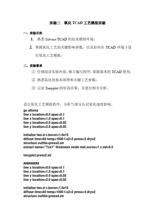
实验二氧化TCAD工艺模拟实验一、实验目的1. 熟悉Silvaco TCAD的仿真模拟环境;2.掌握氧化工艺的关键影响参数,以及如何在TCAD环境下进行氧化工艺模拟;二、实验要求①仔细阅读实验内容,独立编写程序,掌握基本的TCAD使用;②熟悉氧化的基本原理和关键工艺参数;③记录Tonyplot的仿真结果,并进行相关分析。
设计氧化工艺模拟程序,分析气体分压对氧化速度影响。
go athenaline x location=0.0 spac=0.1line x location=1.0 spac=0.1line y location=0.0 spac=0.05line y location=2.0 spac=0.05initialize two.d c.boron=1.0e15diffuse time=60 temp=1000 f.o2=2 press=2 dryo2structure outfile=press2.strextract name="Tox1" thickness oxide mat.occno=1 x.val=0.5tonyplot press2.str#########line x location=0.0 spac=0.1line x location=1.0 spac=0.1line y location=0.0 spac=0.05line y location=2.0 spac=0.05initialize two.d c.boron=1.0e15diffuse time=60 temp=1000 f.o2=2 press=4 dryo2structure outfile=press4.strextract name="Tox2" thickness oxide mat.occno=1 x.val=0.5 tonyplot press4.str##############line x location=0.0 spac=0.1line x location=1.0 spac=0.1line y location=0.0 spac=0.05line y location=2.0 spac=0.05initialize two.d c.boron=1.0e15diffuse time=60 temp=1000 f.o2=2 press=6 dryo2structure outfile=press6.strextract name="Tox3" thickness oxide mat.occno=1 x.val=0.5 tonyplot press6.str########line x location=0.0 spac=0.1line x location=1.0 spac=0.1line y location=0.0 spac=0.05line y location=2.0 spac=0.05initialize two.d c.boron=1.0e15diffuse time=60 temp=1000 f.o2=2 press=8 dryo2structure outfile=press8.strextract name="Tox4" thickness oxide mat.occno=1 x.val=0.5 tonyplot press8.str数据分析:EXTRACT> extract name="Tox1" thickness oxide mat.occno=1 x.val=0.5 Tox1=813.408 angstroms (0.0813408 um) X.val=0.5extract name="Tox2" thickness oxide mat.occno=1 x.val=0.5Tox2=1160.89 angstroms (0.116089 um) X.val=0.5EXTRACT> extract name="Tox3" thickness oxide mat.occno=1 x.val=0.5 Tox3=1466.97 angstroms (0.146697 um) X.val=0.5EXTRACT> extract name="Tox4" thickness oxide mat.occno=1 x.val=0.5Tox4=1739.47 angstroms (0.173947 um) X.val=0.5根据实验数据分析得随着气体分压的加强氧化速度呈上升的趋势。
学生实验报告如图所示,定义npn晶体管的网络信息x为2.0,y为1.0,该区域块掺杂n型材料浓度为5e15,设置为均匀分布;n型材料浓度为1e18,设置为高斯分布,峰值为1.0;p型材料浓度为1e18,设置为高斯分布,峰值为0.05,结深为0.15;n型材料浓度为5e19,设置为高斯分布,峰值为0,结深为0.05,在x的右边区域0.8处;p型材料浓度为5e19,设置为高斯分布,峰值为0,在x的左边区域0.8处,从而形成了该结构,包括N+区域,P+区域,P区域,N-区域,N区域图一器件结构2、网格调用及设计#调用atlas器件仿真器go atlas#网络mesh初始化Mesh#定义x方向网格信息x.m l=0 spacing=0.15x.m l=0.8 spacing=0.15x.m l=1.0 spacing=0.03x.m l=1.5 spacing=0.12x.m l=2.0 spacing=0.15#定义y方向网格信息y.m l=0.0 spacing=0.006y.m l=0.04 spacing=0.006y.m l=0.06 spacing=0.005y.m l=0.15 spacing=0.02y.m l=0.30 spacing=0.02y.m l=1.0 spacing=0.12#定义区域信息region num=1 silicon#定义电极信息electrode num=1 name=emitter left length=0.8 electrode num=2 name=base right length=0.5 y.max=0 electrode num=3 name=collector bottom#该区域块掺杂n型材料浓度为5e15,设置为均匀分布doping reg=1 uniform n.type conc=5e15# n型材料浓度为1e18,设置为高斯分布,峰值为1.0doping reg=1 gauss n.type conc=1e18 peak=1.0 char=0.2# p型材料浓度为1e18,设置为高斯分布,峰值为0.05,结深为0.15doping reg=1 gauss p.type conc=1e18 peak=0.05 junct=0.15# n型材料浓度为5e19,设置为高斯分布,峰值为0,结深为0.05,在x的右边区域0.8处doping reg=1 gauss n.type conc=5e19 peak=0.0 junct=0.05 x.right=0.8# p型材料浓度为5e19,设置为高斯分布,峰值为0,在x的左边区域0.8处doping reg=1 gauss p.type conc=5e19 peak=0.0 char=0.08 x.left=1.5#set bipolar models#设置BJT仿真所需要用到的物理模型models conmob fldmob consrh auger print#设置接触类型contact name=emitter n.poly surf.rec#求解初始化solve init#保存结构信息文件save outf=bjtex04_0.str#用tonyplot绘图示意结构文件tonyplot bjtex04_0.str -set bjtex04_0.set(二)对比分析表 3-1发射区掺杂浓度不变,改变基区掺杂浓度器件结构与杂质分布图输出曲线浓度(cm-3)1e161e171e181e19表3-2在不同基区掺杂浓度下的参数电流放大系数β浓度(cm3-)最大集电极电流c I(mA)1e16 1.18576 237.1521e17 1.13197 226.3951e18 0.669093 133.8191e19 0.0579857 11.5971实验结论:由表可知,在发射区掺杂浓度不变,改变基区掺杂浓度下,当基区掺杂浓度逐渐增大,最大集电极电流逐渐减小,电流放大系数减小。
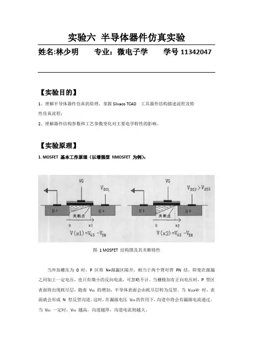
实验六半导体器件仿真实验姓名:林少明专业:微电子学学号11342047【实验目的】1、理解半导体器件仿真的原理,掌握Silvaco TCAD 工具器件结构描述流程及特性仿真流程;2、理解器件结构参数和工艺参数变化对主要电学特性的影响。
【实验原理】1. MOSFET 基本工作原理(以增强型NMOSFET 为例):图 1 MOSFET 结构图及其夹断特性当外加栅压为0 时,P 区将N+源漏区隔开,相当于两个背对背PN 结,即使在源漏之间加上一定电压,也只有微小的反向电流,可忽略不计。
当栅极加有正向电压时,P 型区表面将出现耗尽层,随着V GS的增加,半导体表面会由耗尽层转为反型。
当V GS>V T时,表面就会形成N 型反型沟道。
这时,在漏源电压V DS的作用下,沟道中将会有漏源电流通过。
当V DS一定时,V GS越高,沟道越厚,沟道电流则越大。
2. MOSFET 转移特性V DS 恒定时,栅源电压 V GS 和漏源电流 I DS 的关系曲线即是 MOSFET 的转移特性。
对于增强型 NMOSFET ,在一定的 V DS 下, V GS =0 时, I DS =0;只有 V GS >V T 时,才有 I DS >0。
图 2 为增强型 NMOSFET 的转移特性曲线。
图 2 增强型 NMOSFET 的转移特性曲线图中转折点位置处的 V GS (th ) 值为阈值电压。
3. MOSFET 的输出特性对于 NMOS 器件,可以证明漏源电流:令n =oxWC Lμβ,称β为增益因子。
(1)()DS GS T V V V <<-由于 V DS 很小,忽略2DS V 项,可得:I DS 随 V DS 而线性增加,故称为线性区。
(2)()DS GS T V V V <-DS V 增大,但仍小于()GS T V V -,2DS V 项不能忽略。
故:在一定栅源电压下,V DS 越大,沟道越窄,则沟道电阻越大,曲线斜率变小。
学生实验报告院别课程名称器件仿真与工艺综合设计实验班级实验三MOSFET工艺器件仿真姓名实验时间学号指导教师成绩批改时间报告内容一、实验目的和任务1.理解半导体器件仿真的原理,掌握Silvaco TCAD 工具器件结构描述流程及特性仿真流程;2.理解器件结构参数和工艺参数变化对主要电学特性的影响。
二、实验原理1. MOSEET基本工作原理(以增强型NMOSFET为例):以N沟道MOSEET为例,如图1所示,是MOSFET基木结构图。
在P型半导体衬底上制作两个N+区,其中一个作为源区,另一个作为漏区。
源、漏区之间存在着沟道区,该横向距离就是沟道长度。
在沟道区的表面上作为介质的绝缘栅是由热氧化匸艺生长的二氧化硅层。
在源区、漏区和绝缘栅上的电极是由一层铝淀积,用于引出电极,引出的三个电极分别为源极S、漏极D和栅极G。
并且从MOSEET衬底上引出一个电极B极。
加在四个电极上的电压分别为源极电压Vs、漏极电压V D、栅极电压V G和衬底偏压V B。
图1 MOSFET结构示意图MOSFET在工作时的状态如图2所示。
Vs V D和V B的极性和大小应确保源区与衬底之间的PN结及漏区与衬底之间的PN结处与反偏位置。
可以把源极与衬底连接在一起,并且接地,即Vs=0,电位参考点为源极,则V G、V D可以分别写为(栅源电压)V GS、(漏源电压)V DS。
从MOSFET的漏极流入的电流称为漏极电流ID。
(1)在N沟道MOSFET中,当栅极电压为零时,N+源区和N+漏区被两个背靠背的二极管所隔离。
这时如果在漏极与源极之间加上电压V DS,只会产生PN 结反向电流且电流极其微弱,其余电流均为零。
(2)当栅极电压V GS不为零时,栅极下面会产生一个指向半导体体内的电场。
(3)当V GS增大到等于阈值电压V T的值时,在半导体内的电场作用下,栅极下的P型半导体表面开始发生强反型,因此形成连通N+源区和N+漏区的N型沟道,如图2所示。
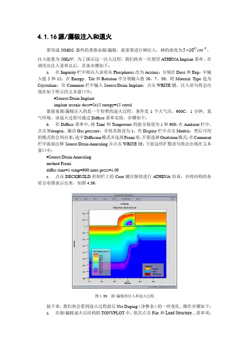
4.1.16源/漏极注入和退火要形成NMOS 器件的重掺杂源/漏极,就需要进行砷注入。
砷的浓度为153510cm -⨯,注入能量为50KeV 。
为了演示这一注入过程,我们将再一次使用ATHENA Implant 菜单。
在调用出注入菜单以后,具体步骤如下:a. 在Impurity 栏中将注入杂质从Phosphorus 改为Arsenic ;分别在Dose 和Exp :中输入值5和15;在Energy 、Tilt 和Rotation 中分别输入值50、7、30;将Material Type 选为Crystalline ;在Comment 栏中输入Source/Drain Implant ;点击WRITE 键,注入语句将会出现在如下所示的文本窗口中:#Source/Drain Implantimplant arsenic dose=5e15 energy=15 crytal紧接着源/漏极注入的是一个短暂的退火过程,条件是1个大气压,900C ,1分钟,氮气环境。
该退火过程可通过Diffuse 菜单实现,步骤如下:b. 在Diffuse 菜单中,将Time 和Tempreture 的值分别设为1和900;在Ambient 栏中,点击Nitrogen ;激活Gas pressure ,并将其值设为1;在Display 栏中点击Models ,然后可用的模式将会列出来;选中Diffusion 模式并选择Fermi 项。
不要选择Oxidation 模式;在Comment 栏中添加注释Source/Drain Annealing 并点击WRITE 键;下面这些扩散语句将会出现在文本窗口中:#Source/Drain Annealingmethod Fermidiffus time=1 temp=900 nitro press=1.00c. 点击DECKBUILD 控制栏上的Cont 键以继续进行ATHENA 仿真,并将结构的杂质分布图表示出来,如图4.39;图4.39 源/漏极的注入和退火过程接下来,我们将会看到退火过程前后Net Doping (净掺杂)的一些变化。
Silvaco TCAD基CMOS器件仿真毕业设计目录1 引言 (1)1.1 MOSFET的发展 (1)1.2 TCAD的发展 (3)2 MOSFET的基本构造及工作原理 (4)2.1 MOSFET的基本原理及构造 (4)2.2 MOSFET的基本工作原理 (5)2.3 MOSFET的~I V特性 (9)3 TCAD工具的构成、仿真原理、仿真流程及仿真结果 (11)3.1 TCAD工具的结构与仿真原理 (11)3.2 用TCAD工具仿真NMOS的步骤 (11)3.3 TCAD工具的仿真结果 (15)4 结论 (16)谢辞 (17)参考文献 (19)附录 (21)正文:1 引言在当今时代,集成电路发展十分迅猛,其工艺的发杂度不断提高,开发新工艺面临着巨大的挑战。
传统的开发新工艺的方法是工艺试验,而现在随着工艺开发的工序细化,流片周期变长,传统的方法已经不能适应现在的需要,这就需要寻找新的方法来解决这个问题。
幸运的是随着计算机性能和计算机技术的发展,人们结合所学半导体理论与数值模拟技术,以计算机为平台进行工艺与器件性能的仿真。
现如今仿真技术在工艺开发中已经取代了工艺试验的地位。
采用TCAD 仿真方式来完成新工艺新技术的开发,突破了标准工艺的限制,能够模拟寻找最合适的工艺来完成自己产品的设计。
此外,TCAD仿真能够对器件各种性能之间存在的矛盾进行同时优化,能够在最短的时间以最小的代价设计出性能符合要求的半导体器件。
进行新工艺的开发,需要设计很多方面的容,如:进行器件性能与结构的优化、对器件进行模型化、设计进行的工艺流程、提取器件模型的参数、制定设计规则等等。
为了设计出质量高且价格低廉的工艺模块,要有一个整体的设计目标,以它为出发点将工艺开发过程的各个阶段进行联系,本着简单易造的准则,系统地进行设计的优化。
TCAD支持器件设计、器件模型化和工艺设计优化,使得设计思想可以实现全面的验证。
TCAD设计开发模拟是在虚拟环境下进行的,缩短了开发周期,降低了开发成本,是一条高效低成本的进行新工艺研究开发的途径。
半导体专业实验补充silvac o器件仿真————————————————————————————————作者:————————————————————————————————日期:实验2 PN结二极管特性仿真1、实验内容(1)PN结穿通二极管正向I-V特性、反向击穿特性、反向恢复特性等仿真。
(2)结构和参数:PN结穿通二极管的结构如图1所示,两端高掺杂,n-为耐压层,低掺杂,具体参数:器件宽度4μm,器件长度20μm,耐压层厚度16μm,p+区厚度2μm,n+区厚度2μm。
掺杂浓度:p+区浓度为1×1019cm-3,n+区浓度为1×1019cm-3,耐压层参考浓度为5×1015cm-3。
0 Wp n n图1普通耐压层功率二极管结构2、实验要求(1)掌握器件工艺仿真和电气性能仿真程序的设计(2)掌握普通耐压层击穿电压与耐压层厚度、浓度的关系。
3、实验过程#启动Athenago athena#器件结构网格划分;line x loc=0.0 spac=0.4line x loc=4.0 spac= 0.4lineyloc=0.0spac=0.5line y loc=2.0 spac=0.1line y loc=10spac=0.5line y loc=18spac=0.1line y loc=20 spac=0.5#初始化Si衬底;initsilicon c.phos=5e15 orientation=100 two.d#沉积铝;deposit alum thick=1.1div=10#电极设置electrode name=anode x=1electrodename=cathode backside#输出结构图structureoutf=cb0.strtonyplotcb0.str#启动Atlasgo atlas#结构描述doping p.typeconc=1e20 x.min=0.0 x.max=4.0 y.min=0y.max=2.0 uniformdopingn.type conc=1e20x.min=0.0 x.max=4.0y.min=18y.max=20.0 uniform#选择模型和参数models cvt srh printmethod carriers=2impact selb#选择求解数值方法methodnewton#求解solve initlog outf=cb02.logsolve vanode=0.03solve vanode=0.1vstep=0.1 vfinal=5 name=anode#画出IV特性曲线tonyplot cb02.log#退出quit图2为普通耐压层功率二极管的仿真结构。
半导体工艺专业实践报告实践报告 - 半导体工艺专业[正文]一、引言半导体工艺学作为现代电子工程中的核心课程,探索了半导体材料的特性、半导体器件制造过程以及相关设备和技术。
本实践报告旨在总结并分享我在半导体工艺专业实践中的所学所悟,以及对未来发展的展望。
二、实践经历与成果1. 实验一:半导体材料特性研究在实验室中,我们利用光致发光(PL)技术和X射线衍射(XRD)技术研究了半导体材料的发光性能和晶体结构,深入了解了材料的能带结构以及载流子的行为。
通过实验,我进一步巩固了关于半导体材料的理论知识,并学会了熟练操作相关设备。
2. 实验二:半导体器件制造在器件制造实验中,我们使用光刻技术、湿法腐蚀和离子注入技术制备了p-n结器件。
在整个制造过程中,我非常重视每个步骤的操作细节,以确保器件制造的精度和可靠性。
在实践中,我还学会了如何评估器件的质量,并提出改进建议。
3. 实验三:设备调试与维护在设备调试与维护实验中,我们学习了半导体设备的基本原理,并掌握了设备调试和故障排除的技巧。
通过实践,我学会了如何操作并维护薄膜沉积设备、离子注入设备和蒸发设备等,并对实验室设备的正常运行起到了积极的辅助作用。
4. 实验四:半导体工艺流程设计在工艺流程设计实验中,我们根据不同器件的要求设计了相应的工艺流程,并利用软件进行了模拟和优化。
通过这个实验,我更加了解了不同工艺参数对器件性能的影响,并培养了分析和解决工艺问题的能力。
三、项目反思与展望通过半导体工艺专业的实践,我不仅掌握了半导体材料特性研究的方法和技术,还熟悉了半导体器件制造的过程和工艺流程的设计。
在今后的学习和研究中,我希望能进一步深入了解先进的半导体材料、器件和工艺技术,为行业的发展做出更多的贡献。
结语半导体工艺专业的实践让我对半导体材料和器件制造有了更深入的认识,并培养了实验操作和问题解决的能力。
我相信这些实践经历将对我未来的学习和职业发展产生积极的影响,使我能够更好地应对半导体工艺领域的挑战。
4.1.10多晶硅栅的淀积淀积可以用来产生多层结构。
共形淀积是最简单的淀积方式,并且在各种淀积层形状要求不是非常严格的情况下使用。
NMOS工艺中,多晶硅层的厚度约为2000 Å,因此可以使用共形多晶硅淀积来完成。
为了完成共形淀积,从ATHENA Commands菜单中依次选择Process、Deposit和Deposit…菜单项。
ATHENA Deposit菜单如图4.30所示;a.在Deposit菜单中,淀积类型默认为Conformal;在Material菜单中选择Polysilicon,并将它的厚度值设为0.2;在Grid specification参数中,点击Total number of layers并将其值设为10。
(在一个淀积层中设定几个网格层通常是非常有用的。
在这里,我们需要10个网格层用来仿真杂质在多晶硅层中的传输。
)在Comment一栏中添加注释Conformal Polysilicon Deposition,并点击WRITE键;b.下面这几行将会出现在文本窗口中:#Conformal Polysilicon Deposition图4.30 ATHENA 淀积菜单deposit polysilicon thick=0.2 divisions=10c.点击DECKBUILD控制栏上的Cont键继续进行A THENA仿真;d.还是通过DECKBUILD Tools菜单的Plot和Plot structure…来绘制当前结构图。
创建后的三层结构如图4.31所示。
图4.31 多晶硅层的共形淀积4.1.11简单的几何图形刻蚀接下来就是多晶硅的栅极定义。
这里我们将多晶硅栅极的左边边缘定为x=0.35μm,中心定为x=0.6μm。
因此,多晶硅应从左边x=0.35μm开始进行刻蚀,如图4.32所示。
图4.32 ATHENA Etch菜单a.在DECKBUILD Commands菜单中依次选择Process、Etch和Etch…。
Indium Implant and Anneal1 go athena23 #TITLE: Indium Anneal45 #the x dimension definition6 line x loc = 0.0 spacing=0.17 line x loc = 0.1 spacing=0.189 #the vertical definition10 line y loc = 0 spacing = 0.0211 line y loc = 2.0 spacing = 0.201213 #initialize the mesh14 init silicon c.phos=1.0e141516 #perform uniform boron implant17 implant indium dose=1e13 energy=70 monte18 structure outfile=andfex12_0.str1920 #perform diffusion21 diffuse time=30 temperature=1000222324 extract name="xj" xj silicon mat.occno=1 x.val=0.0 junc.occno=12526 #save the structure27 structure outfile=andfex12_1.str2829 tonyplot -overlay andfex12_0.str andfex12_1.str -set andfex12.set3031 quitOxidation Enhanced Diffusion of Boron1 go athena23 # OED of Boron45 #the x dimension definition6 line x loc = 0.0 spacing=0.17 line x loc = 0.1 spacing=0.189 #the vertical definition10 line y loc = 0 spacing = 0.0211 line y loc = 2.0 spacing = 0.2012 line y loc = 25.0 spacing = 2.51314 #initialize the mesh15 init silicon c.boron=1.0e141617 #perform uniform boron implant18 implant boron dose=1e13 energy=701920 #set diffusion model for OED21 method two.dim2223 #perform diffusion24 diffuse time=30 temperature=1000 dryo225 #26 extract name="xj_two.dim" xj silicon mat.occno=1 x.val=0.0 junc.occno=12728 #save the structure29 structure outfile=andfex02_0.str3031 # repeat the simulation with default FERMI model32 go athena3334 #TITLE: Simple Boron Anneal3536 #the x dimension definition37 line x loc = 0.0 spacing=0.138 line x loc = 0.1 spacing=0.13940 #the vertical definition41 line y loc = 0 spacing = 0.0242 line y loc = 2.0 spacing = 0.2043 line y loc = 25.0 spacing = 2.54445 #initialize the mesh46 init silicon c.phos=1.0e144748 #perform uniform boron implant49 implant boron dose=1e13 energy=705051 #select diffusion model52 method fermi5354 #perform diffusion55 diffuse time=30 temperature=1000 dryo256 #57 extract name="xj_fermi" xj silicon mat.occno=1 x.val=0.0 junc.occno=1585960 #save the structure61 structure outfile=andfex02_1.str6263 # compare diffusion models64 tonyplot -overlay andfex02_0.str andfex02_1.str -set andfex02.set Emitter Push Effect1 go athena23 #TITLE: Emitter push effect example4 #5 line x loc=0.0 spac=0.26 line x loc=2.5 spac=0.87 line x loc=3.0 spac=0.28 #9 line y loc=0.00 spac=0.0410 line y loc=0.3 spac=0.0611 line y loc=2.0 spac=0.812 line y loc=10.0 spac=2.013 #14 init c.phos=1e1515 #16 implant boron dose=1e13 energy=4017 #18 deposit nitride thick=.2 div=419 #20 etch right nitride p1.x=2.521 relax y.min=1.522 #23 implant phosphor dose=1e16 energy=3024 #25 etch nitride all26 #27 method compress full.cpl28 diffuse time=30 temp=100029 #30 structure outfile=andfex07.str31 #32 tonyplot -st andfex07.str -set andfex07.set3334 quitDamage Enhanced Diffusion of ArsenicThis example demonstrates the damage enhanced diffusion effect in a heavy arsenic implant typical of MOS source/drain or bipolar emitter processing.1 go athena23 #the x dimension definition4 line x loc = 0.0 spacing=0.15 line x loc = 0.1 spacing=0.167 #the vertical definition8 line y loc = 0 spacing = 0.0059 line y loc = 2.0 spacing = 0.2010 line y loc = 25.0 spacing = 2.51112 #initialize the mesh13 init silicon c.boron=1.0e171415 #deposit screen oxide16 deposit oxide thickness=0.005 div=21718 #perform arsenic implant with damage19 implant arsenic dose=1.0e15 energy=40 tilt=7 unit.damage dam.factor=0.12021 #set diffusion model for TED22 method full.cpl2324 #perform diffusion25 diffuse time=15/60 temperature=100026 #27 extract name="xj_fullcpl" xj silicon mat.occno=1 x.val=0.0 junc.occno=12829 #save the structure30 structure outfile=andfex03_0.str3132 # repeat the simulation with FERMI model3334 #the x dimension definition35 line x loc = 0.0 spacing=0.136 line x loc = 0.1 spacing=0.13738 #the vertical definition39 line y loc = 0 spacing = 0.00540 line y loc = 2.0 spacing = 0.2041 line y loc = 25.0 spacing = 2.54243 #initialize the mesh44 init silicon c.boron=1.0e174546 #deposit screen oxide47 deposit oxide thickness=0.005 div=24849 #perform arsenic implant with damage50 implant arsenic dose=1.0e15 energy=40 tilt=7 unit.damage dam.factor=0.15152 #set default model53 method fermi5455 #perform diffusion56 diffuse time=15/60 temperature=100057 #58 extract name="xj_fermi" xj silicon mat.occno=1 x.val=0.0 junc.occno=15960 #save the structure61 structure outfile=andfex03_1.str6263 # compare diffusion models64 tonyplot -overlay andfex03_0.str andfex03_1.str -set andfex03.set。
实验2 PN结二极管特性仿真1、实验内容(1PN结穿通二极管正向I-V特性、反向击穿特性、反向恢复特性等仿真。
(2结构和参数:PN结穿通二极管的结构如图1所示,两端高掺杂,n-为耐压层,低掺杂,具体参数:器件宽度4μm,器件长度20μm,耐压层厚度16μm,p+区厚度2μm,n+区厚度2μm。
掺杂浓度:p+区浓度为1×1019cm-3,n+区浓度为1×1019cm-3,耐压层参考浓度为5×1015 cm-3。
图1 普通耐压层功率二极管结构2、实验要求(1掌握器件工艺仿真和电气性能仿真程序的设计(2掌握普通耐压层击穿电压与耐压层厚度、浓度的关系。
3、实验过程#启动Athenago athena#器件结构网格划分;line x loc=0.0 spac= 0.4line x loc=4.0 spac= 0.4line y loc=0.0 spac=0.5line y loc=2.0 spac=0.1line y loc=10 spac=0.5line y loc=18 spac=0.1line y loc=20 spac=0.5#初始化Si衬底;init silicon c.phos=5e15 orientation=100 two.d #沉积铝;deposit alum thick=1.1 div=10#电极设置electrode name=anode x=1electrode name=cathode backside#输出结构图structure outf=cb0.strtonyplot cb0.str#启动Atlasgo atlas#结构描述doping p.type conc=1e20 x.min=0.0 x.max=4.0 y.min=0 y.max=2.0 uniformdoping n.type conc=1e20 x.min=0.0 x.max=4.0 y.min=18 y.max=20.0 uniform#选择模型和参数models cvt srh printmethod carriers=2impact selb#选择求解数值方法method newton#求解solve initlog outf=cb02.logsolve vanode=0.03solve vanode=0.1 vstep=0.1 vfinal=5 name=anode#画出IV特性曲线tonyplot cb02.log#退出quit图2为普通耐压层功率二极管的仿真结构。