基于ADF4360-0的微波扫频信号发生器设计
- 格式:pdf
- 大小:282.89 KB
- 文档页数:5
一种高精度正弦波扫频信号发生器的设计与实现关 宇1,吴 巍2,尹廷辉3(1.解放军理工大学理学院电子线路教研室,江苏省南京市210007;2.东南大学医学院,江苏省南京市210096;3.解放军理工大学通信工程学院电子技术教研室,江苏省南京市210007)第30卷第2期 2004年2月 电子工程师 EL ECTRON IC EN GIN EER Vol.30No.2 Feb.2004【摘 要】 作为一种新型外科手术器械,超声刀正在多个外科领域得到越来越多的应用。
超声刀是一种功率超声波发生器,不同用途的超声刀工作于不同的频段,早期的超声刀都是针对某种人体组织设计的单频专用手术装置。
提出了一种适用于多功能超声手术装置的正弦波扫频信号发生器。
该信号发生器以单片机为控制核心,采用数字混频和自适应滤波技术,用高、低两个频率分别控制扫频信号的频带和分辨率的方案,解决了实现扫频电路中高频、窄带、高分辨率等指标的难题,为类似问题的解决提供了一种可选方案。
该方案已成功用于“N T Y300型多功能超声手术装置”项目,该项目获得国家科技进步三等奖。
关键词:扫频信号发生器,功率超声波,超声刀,振荡器,数字混频器,自适应滤波器中图分类号:TN752.6收稿日期:2003209215;修回日期:20042022020 引 言超声刀作为一种新型手术器械,正在多个外科领域得到越来越多的应用。
不同形式的超声刀可以用于脑外科的颅骨切割、腹外科的肝脏手术、眼科的白内障切除和心血管外科的血栓消融。
与常规手术器械相比,具有创伤小、出血量低等优点,是一种很有前途的手术装置[1]。
超声刀是一种功率超声波发生器。
功率超声波作用于人体组织时,会在组织内产生空化效应,造成局部组织的破坏和分离,而对周围组织的影响较小[2]。
研究表明,不同的人体组织对超声波能量的吸收具有频率选择性[3],用于不同手术部位的超声刀必须工作于相应的频带。
早期的超声刀都是针对某种人体组织设计的单频专用手术装置[4],为了达到一机多用的目的,研制适用于不同组织的多功能超声手术装置势在必行。
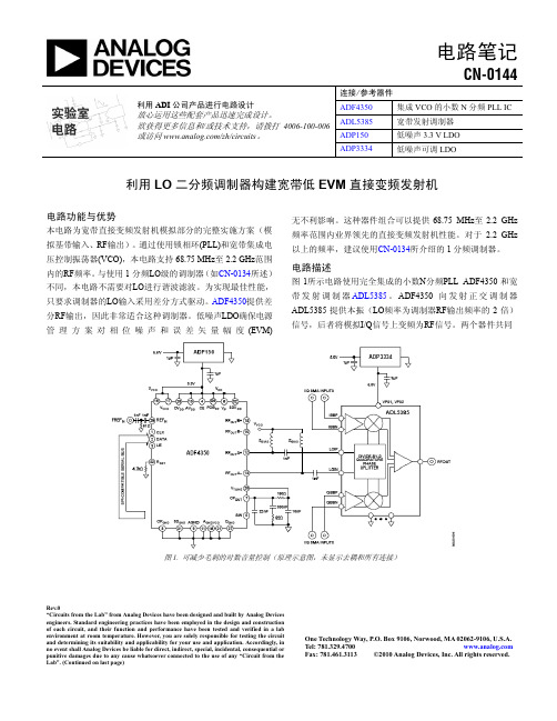
电路笔记CN-0144连接/参考器件ADF4350 集成VCO的小数N分频PLL ICADL5385 宽带发射调制器ADP150 低噪声3.3 V LDO利用ADI公司产品进行电路设计放心运用这些配套产品迅速完成设计。
欲获得更多信息和/或技术支持,请拨打4006-100-006或访问/zh/circuits。
ADP3334 低噪声可调LDORev.0“Circuits from the Lab” from Analog Devices have been designed and built by Analog Devicesengineers. Standard engineering practices have been employed in the design and constructionof each circuit, and their function and performance have been tested and verified in a labenvironment at room temperature. However, you are solely responsible for testing the circuitand determining its suitability and applicability for your use and application. Accordingly, inno event shall Analog Devices be liable for direct, indirect, special, incidental, consequential orOne Technology Way, P.O. Box 9106, Norwood, MA 02062-9106, U.S.A.Tel: Fax: 781.461.3113©2010 Analog Devices, Inc. All rights reserved.利用LO二分频调制器构建宽带低EVM直接变频发射机电路功能与优势本电路为宽带直接变频发射机模拟部分的完整实施方案(模拟基带输入、RF输出)。
基于ADF4360-1的2.4G频率合成器设计摘要:该文通过高性能、低功耗的8位ATmega8微处理器产生控制信号,利用美国ADI公司生产的锁相环芯片ADF4360-1,设计了一个稳定的2.4GHz本振信号源电路模块,可广泛应用于电视,仪器,通信等领域。
文中详细介绍了系统中核心芯片的性能、结构以及应用方法,设计出了完整的硬件电路并对电路的各个参数进行了评估,结果基本上符合要求。
关键词:ATmega8 ADF4360-1锁相环频率合成本振信号源在现代无线电通信及相关领域中,为确保通信的稳定和可靠,对通信设备的频率准确度和稳定度提出了越来越高的要求。
与LC振荡电路“跑频”严重相比,晶体振荡电路具有可微调的稳定频率,但变化范围小,频率值不高。
频率合成技术是指将一个或少量的高稳定度、高准确度的标准频率作为参考频率,经过相应的信号处理过程,从而获得大量离散的具有同一稳定度和准确度的信号频率。
主要有三种合成方法:直接模拟合成、锁相环合成以及直接数字合成。
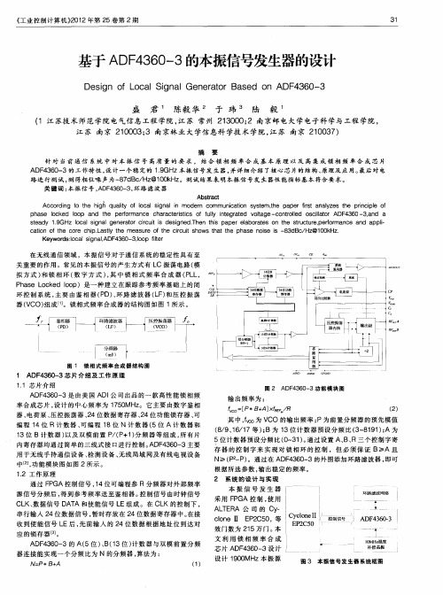
1 锁相式频率合成器的基本原理锁相环路(PLL)具有较为突出的优点:频率在一定范围内可调;数字化接口;能实现快速准确的跳频通信;抗干扰能力强。
锁相环频率合成器通过锁相环完成频率的加减乘除运算,是一种建立在相位负反馈基础上的闭环控制系统,对相位噪声和杂散具有很好的抑制作用。
原理图如图1所示,主要由鉴相器、环路滤波器和压控振荡器组成。
外部晶振提供的参考频率信号与压控振荡器的输出频率经程序N分频后在鉴相器内进行相位比较,产生误差控制电压,再经环路滤波器滤除误差信号中的噪声和高频分量,最后输出的直流脉冲电压控制压控振荡器产生所需的振荡频率。
通过锁相式频率合成实现的频率源应用广泛于通信、电视等电子设计领域,重点用于以下三方面:接收机本地振荡;发射机载波信号;信号发生器。
ADI公司生产的ADF4360-1内置可编程分频器,具有电荷泵电流编程功能,可应用于无线射频通信系统,是一款性价比很高的电荷泵锁存芯片。

基于DSP的微波信号源控制张庆彪;郭高凤;李恩【摘要】In order to realize the miniaturization and portability of signal source, using DSP TMS320LF2407A with pulse width modulation (PWM) function of the pins to implement the control of microwave signal source. According to mathemati-cal relationship and clock relations, the ADF4156 is controlled by outputting three synchronous clock control signals CLOCK, DATA and LE, so as to control the sweeping frequency of microwave signal source. The experiments about that control signal test using oscillometer and signal source test using spectrum analyzer are performed, whose corresponding relation of the con-trol signal in time domain, the frequency signal's power in the frequency spectrum analyzer and the signal movement process in the whole frequency range can be gained. Test results show that the signal source's sweeping frequency can be implemented by output control signal. It has characteristics of adjustable sweeping frequency speed and flexible button.%为了实现信号源的小型化,便携性,采用DSP芯片TMS320LF2407A利用具有脉宽调制(PWM)功能的引脚,根据芯片资料中控制信号的数学关系式和时钟关系,编程实现输出3路同步时钟控制信号CLOCK,DATA,LE控制AD公司频率合成芯片ADF4156的方法来控制微波信号源的点频扫频等动作.做了示波器测试控制信号,频谱仪测试信号源实验,可以清晰地看到控制信号在时域上的对应关系以及频谱仪中所设置频率信号的功率以及信号在整个频段的移动过程.结果表明输出的控制信号能够精确地使信号源实现点频和扫频功能,具有控制时钟,扫频速度可调,按键控制灵活的特点.【期刊名称】《现代电子技术》【年(卷),期】2011(034)018【总页数】3页(P15-17)【关键词】DSP脉宽调制;PWM;微波信号源;锁相环频率合成【作者】张庆彪;郭高凤;李恩【作者单位】电子科技大学,四川成都611731;电子科技大学,四川成都611731;电子科技大学,四川成都611731【正文语种】中文【中图分类】TN919-340 引言微波信号源采用锁相环频率合成器设计,工作频率范围为4~6 GHz。
Integrated Synthesizer and VCOADF4360-0 Rev.0Information furnished by Analog Devices is believed to be accurate and reliable.However, no responsibility is assumed by Analog Devices for its use, nor for anyinfringements of patents or other rights of third parties that may result from its use. Specifications subject to change without notice. No license is granted by implication or otherwise under any patent or patent rights of Analog Devices. Trademarks and registered trademarks are the property of their respective owners.One Technology Way, P.O. Box 9106, Norwood, MA 02062-9106, U.S.A. Tel: Fax: 781.326.8703© 2004 Analog Devices, Inc. All rights reserved.FEATURESOutput frequency range: 2400 MHz to 2725 MHz Divide-by-2 output3.0 V to 3.6 V power supply1.8 V logic compatibilityInteger-N synthesizerProgrammable dual-modulus prescaler 16/17, 32/33 Programmable output power level3-wire serial interfaceAnalog and digital lock detectHardware and software power-down mode APPLICATIONSWireless handsets (DECT, GSM, PCS, DCS, WCDMA) Test equipmentWireless LANsCATV equipment GENERAL DESCRIPTIONThe ADF4360-0 is a fully integrated integer-N synthesizer and voltage controlled oscillator (VCO). The ADF4360-0 is designed for a center frequency of 2600 MHz. In addition, a divide-by-2 option is available, whereby the user gets an RF output of be-tween 1200 MHz and 1360 MHz.Control of all the on-chip registers is through a simple 3-wire interface. The device operates with a power supply ranging from 3.0 V to 3.6 V and can be powered down when not in use.FUNCTIONAL BLOCK DIAGRAMVCO REFTUNEC CC NOUT AOUT BFigure 1.ADF4360-0Rev. 0 | Page 2 of 20TABLE OF CONTENTSSpecifications.....................................................................................3 Timing Characteristics.....................................................................5 Absolute Maximum Ratings............................................................6 Transistor Count...........................................................................6 ESD Caution..................................................................................6 Pin Configuration and Function Descriptions.............................7 Typical Performance Characteristics.............................................8 Circuit Description...........................................................................9 Reference Input Section...............................................................9 Prescaler (P/P + 1)........................................................................9 A and B Counters.........................................................................9 R Counter......................................................................................9 PFD and Charge Pump................................................................9 MUXOUT and Lock Detect......................................................10 Input Shift Register.....................................................................10 VCO.............................................................................................10 Output Stage................................................................................11 Latch Structure...........................................................................12 Control Latch..............................................................................16 N Counter Latch.........................................................................17 R Counter Latch.........................................................................17 Applications.....................................................................................18 Fixed Frequency LO...................................................................18 Power-Up.....................................................................................18 Interfacing...................................................................................18 PCB Design Guidelines for Chip Scale Package...........................19 Output Matching........................................................................19 Outline Dimensions.......................................................................20 Ordering Guide.. (20)REVISION HISTORY7/04—Revision 0: Initial VersionADF4360-0Rev. 0 | Page 3 of 20SPECIFICATIONS 1AV DD = DV DD = V VCO = 3.3 V ± 10%; AGND = DGND = 0 V; T A = T MIN to T MAX , unless otherwise noted. Table 1.Parameter B Version Unit Conditions/Comments REF IN CHARACTERISTICS REF IN Input Frequency 10/250 MHz min/max For f < 10 MHz, use dc-coupledCMOS compatible square wave, slew rate > 21 V/µs.REF IN Input Sensitivity 0.7/AV DD V p-p min/max AC-coupled. 0 to AV DD V max CMOS compatible. REF IN Input Capacitance 5.0 pF max REF IN Input Current ±100 µA max PHASE DETECTORPhase Detector Frequency 28 MHz max CHARGE PUMPI CP Sink/Source 3With R SET = 4.7 kΩ. High Value 2.5 mA typ Low Value 0.312 mA typ R SET Range 2.7/10 kΩ I CP Three-State Leakage Current 0.2 nA typ Sink and Source Current Matching 2 % typ 1.25 V ≤ V CP ≤ 2.5 V. I CP vs. V CP 1.5 % typ 1.25 V ≤ V CP ≤ 2.5 V. I CP vs. Temperature 2 % typ V CP = 2.0 V. LOGIC INPUTS V INH , Input High Voltage 1.5 V min V INL , Input Low Voltage 0.6 V max I INH /I INL , Input Current ±1 µA max C IN , Input Capacitance 3.0 pF max LOGIC OUTPUTS V OH , Output High Voltage DV DD – 0.4 V min CMOS output chosen. I OH , Output High Current 500 µA max V OL , Output Low Voltage 0.4 V max I OL = 500 µA. POWER SUPPLIES AV DD 3.0/3.6 V min/V max DV DD AV DD V VCO AV DD AI DD 410 mA typDI DD 4 2.5 mA typ I VCO 4, 519.0 mA typ I CORE = 10 mA.I RFOUT 43.5 to 11.0 mA typ RF output stage is programmable.Low Power Sleep Mode 47 µA typ RF OUTPUT CHARACTERISTICS 5 VCO Output Frequency 2400/2725 MHz min/max I CORE = 15 mA. VCO Sensitivity 56 MHz/V typ Lock Time 6250 µs typ To within 10 Hz of final frequency. Frequency Pushing (Open Loop) 1 MHz/V typ Frequency Pulling (Open Loop) 15 kHz typ Into 2.00 VSWR load. Harmonic Content (Second) −30 dBc typ Harmonic Content (Third) −39 dBc typOutput Power 5, 7−13/−6.5 dBm typ Programmable in 3 dB steps. See Table 7. Output Power Variation ±3 dB typ For tuned loads, see Output Matching section. VCO Tuning Range 1.25/2.50 V min/max VCO Tuning Port Leakage Current 0.2 nA typADF4360-0Rev. 0 | Page 4 of 20Parameter B Version Unit Conditions/CommentsNOISE CHARACTERISTICS 5VCO Phase Noise Performance 8−111 dBc/Hz typ @ 100 kHz offset from carrier. −133 dBc/Hz typ @ 1 MHz offset from carrier. −140 dBc/Hz typ @ 3 MHz offset from carrier. −145 dBc/Hz typ @ 10 MHz offset from carrier.Synthesizer Phase Noise Floor 9−172 dBc/Hz typ @ 25 kHz PFD frequency. −163 dBc/Hz typ @ 200 kHz PFD frequency. −147 dBc/Hz typ @ 8 MHz PFD frequency. In-Band Phase Noise 10, 11−80 dBc/Hz typ @ 1 kHz offset from carrier.RMS Integrated Phase Error 121.4 Degrees typ 100 Hz to 100 kHz.Spurious Signals due to PFD Frequency 11, 13−75 dBc typ Level of Unlocked Signal with MTLD Enabled −45 dBm typ1 Operating temperature range is: –40°C to +85°C.2Guaranteed by design. Sample tested to ensure compliance. 3I CP is internally modified to maintain constant loop gain over the frequency range. 4T A = 25°C; AV DD = DV DD = V VCO = 3.3 V; P = 32. 5These characteristics are guaranteed for VCO core power = 10 mA. 6Jumping from 2.4 GHz to 2.725 GHz. PFD frequency = 200 kHz; loop bandwidth = 10 kHz. 7Using 50 Ω resistors to V VCO , into a 50 Ω load. For tuned loads, see Output Matching. 8The noise of the VCO is measured in open-loop conditions. 9The synthesizer phase noise floor is estimated by measuring the in-band phase noise at the output of the VCO and subtracting 20 log N (where N is the N divider value). 10The phase noise is measured with the EVAL-ADF4360-xEB1 Evaluation Board and the HP8562E Spectrum Analyzer. The spectrum analyzer provides the REFIN for the synthesizer; offset frequency = 1 kHz. 11f REFIN = 10 MHz; f PFD = 200 kHz; N = 2600; Loop B/W = 10 kHz. 12f REFIN = 10 MHz; f PFD = 1 MHz; N = 2600; Loop B/W = 25 kHz. 13The spurious signals are measured with the EVAL-ADF4360-xEB1 Evaluation Board and the HP8562E Spectrum Analyzer. The spectrum analyzer provides the REFIN for the synthesizer; f REFOUT = 10 MHz @ 0 dBm.ADF4360-0Rev. 0 | Page 5 of 20TIMING CHARACTERISTICSAV DD = DV DD = V VCO = 3.3 V ± 10%; AGND = DGND = 0 V; 1.8 V and 3 V logic levels used; T A = T MIN to T MAX , unless otherwise noted. Table 2.Parameter Limit at T MIN to T MAX (B Version) Unit Test Conditions/Comments t 1 20 ns min LE Setup Timet 2 10 ns min DATA to CLOCK Setup Time t 3 10 ns min DATA to CLOCK Hold Time t 4 25 ns min CLOCK High Duration t 5 25 ns min CLOCK Low Duration t 6 10 ns min CLOCK to LE Setup Time t 720ns minLE Pulse WidthCLOCKDATALELEFigure 2. Timing DiagramADF4360-0Rev. 0 | Page 6 of 20ABSOLUTE MAXIMUM RATINGST A = 25°C, unless otherwise noted. Table 3.Parameter Rating AV DD to GND 1−0.3 V to +3.9 V AV DD to DV DD −0.3 V to +0.3 V V VCO to GND −0.3 V to +3.9 V V VCO to AV DD −0.3 V to +0.3 V Digital I/O Voltage to GND −0.3 V to V DD + 0.3 V Analog I/O Voltage to GND −0.3 V to V DD + 0.3 VREF IN to GND −0.3 V to V DD + 0.3 VOperating Temperature Range −40°C to + 85°CStorage Temperature Range −65°C to +150°CMaximum Junction Temperature 150°CCSP θJA Thermal Impedance Paddle Soldered 50°C/W Paddle Not Soldered 88°C/WLead Temperature, Soldering Vapor Phase (60 sec) 215°C Infrared (15 sec) 220°C1GND = AGND = DGND = 0 V.Stresses above those listed under Absolute Maximum Ratingsmay cause permanent damage to the device. This is a stress rat-ing only; functional operation of the device at these or any other conditions above those listed in the operational sections of this specification is not implied. Exposure to absolute maxi-mum rating conditions for extended periods may affect device reliability. This device is a high performance RF integrated circuit with an ESD rating of <1 kV and it is ESD sensitive. Proper precautions should be taken for handling and assembly.TRANSISTOR COUNT 12543 (CMOS) and 700 (Bipolar)ESD CAUTIONESD (electrostatic discharge) sensitive device. Electrostatic charges as high as 4000 V readily accumulate on the human body and test equipment and can discharge without detection. Although this product features proprietary ESD protection circuitry, permanent damage may occur on devices subjected to high energy electrostatic discharges. Therefore, proper ESD precautions are recommended to avoid performance degradation or loss of functionality.ADF4360-0Rev. 0 | Page 7 of 20PIN CONFIGURATION AND FUNCTION DESCRIPTIONSCPGND AV DD AGND RF OUT A RF OUT B V VCO DATA CLK REF IN DGND C N R SETV T U N E A G N D A G N D A G N D A G N D C C C PC EA G N DD V D DM U X O U TL E04644-0-002Figure 3. Pin ConfigurationADF4360-0Rev. 0 | Page 8 of 20TYPICAL PERFORMANCE CHARACTERISTICS–150–160–170–140–130–120–110–100–90–80–70–40–50–60–30–20–1001k10M1M100k 10kFREQUENCY OFFSET (Hz)O U T P U T P O W E R (d B )Figure 4. Open-Loop VCO Phase Noise04644-0-007–145–150–140–135–130–125–120–115–110–105–90–95–100–85–80–75–7010010M 1M100k10k 1000FREQUENCY OFFSET (Hz)O U T P U T P O W E R (d B )Figure 5. VCO Phase Noise, 2600 MHz, 200 kHz PFD, 10 kHz Loop Bandwidth04644-0-008–145–150–140–135–130–125–120–115–110–105–90–95–100–85–80–75–7010010M 1M100k10k 1000FREQUENCY OFFSET (Hz)O U T P U T P O W E R (d B )Figure 6. VCO Phase Noise, 1300 MHz,Divide-by-2 Enabled 200 kHz PFD, 10 kHz Loop BandwidthO U T P U T P O W E R (d B )–90–80–70–60–50–40–30–20–100–2kHz–1kHz2600MHz1kHz2kHzFigure 7. Close-In Phase Noise at 2600 MHz (200 kHz Channel Spacing)O U T P U T P O W E R (d B )–90–80–70–60–50–40–30–20–100Figure 8. Reference Spurs at 2600 MHz(200 kHz Channel Spacing, 10 kHz Loop Bandwidth)O U T P U T P O W E R (d B )–90–80–70–60–50–40–30–20–100–1MHz –0.5MHz 2250MHz 0.5MHz 1MHzFigure 9. Reference Spurs at 2600 MHz(1 MHz Channel Spacing, 25 kHz Loop Bandwidth)ADF4360-0Rev. 0 | Page 9 of 20CIRCUIT DESCRIPTIONREFERENCE INPUT SECTIONThe reference input stage is shown in Figure 10. SW1 and SW2 are normally closed switches. SW3 is normally open. When power-down is initiated, SW3 is closed, and SW1 and SW2 are opened. This ensures that there is no loading of the REF IN pin on power-down.04414-0-010POWER-DOWNFigure 10. Reference Input StagePRESCALER (P/P + 1)The dual-modulus prescaler (P/P + 1), along with the A and B counters, enables the large division ratio, N , to be realized (N = BP + A ). The dual-modulus prescaler, operating at CML levels, takes the clock from the VCO and divides it down to a manage-able frequency for the CMOS A and B counters. The prescaler is programmable. It can be set in software to 8/9, 16/17, or 32/33 and is based on a synchronous 4/5 core. There is a minimum divide ratio possible for fully contiguous output frequencies; this minimum is determined by P , the prescaler value, and is given by (P 2 − P ).A ANDB COUNTERSThe A and B CMOS counters combine with the dual-modulus prescaler to allow a wide range division ratio in the PLL feed-back counter. The counters are specified to work when the pre-scaler output is 300 MHz or less. Thus, with a VCO frequency of 2.5 GHz, a prescaler value of 16/17 is valid, but a value of 8/9 is not valid.Pulse Swallow FunctionThe A and B counters, in conjunction with the dual-modulus prescaler, make it possible to generate output frequencies that are spaced only by the reference frequency divided by R . The VCO frequency equation is()R f A B P f REFIN VCO /×]+×[=where:f VCO is the output frequency of the VCO.P is the preset modulus of the dual-modulus prescaler (8/9, 16/17, and so on).B is the preset divide ratio of the binary 13-bit counter (3 to 8191). A is the preset divide ratio of the binary 5-bit swallow counter (0 to 31). f REFIN is the external reference frequency oscillator.Figure 11. A and B CountersR COUNTERThe 14-bit R counter allows the input reference frequency to be divided down to produce the reference clock to the phase frequency detector (PFD). Division ratios from 1 to 16,383 are allowed.PFD AND CHARGE PUMPThe PFD takes inputs from the R counter and N counter (N = BP + A ) and produces an output proportional to the phase and frequency difference between them. Figure 12 is a simplified schematic. The PFD includes a programmable delay element that controls the width of the antibacklash pulse. This pulse ensures that there is no dead zone in the PFD transfer function and minimizes phase noise and reference spurs. Two bits in the R counter latch, ABP2 and ABP1, control the width of the pulse (see Table 9).2VFigure 12. PFD Simplified Schematic and Timing (In Lock)ADF4360-0Rev. 0 | Page 10 of 20MUXOUT AND LOCK DETECTThe output multiplexer on the ADF4360 family allows the user to access various internal points on the chip. The state of MUXOUT is controlled by M3, M2, and M1 in the function latch. The full truth table is shown in Table 7. Figure 13 shows the MUXOUT section in block diagram form.Lock DetectMUXOUT can be programmed for two types of lock detect: digital and analog. Digital lock detect is active high. When LDP in the R counter latch is set to 0, digital lock detect is set high when the phase error on three consecutive phase detector cycles is less than 15 ns.With LDP set to 1, five consecutive cycles of less than 15 ns phase error are required to set the lock detect. It stays set high until a phase error of greater than 25 ns is detected on any sub-sequent PD cycle.The N-channel open-drain analog lock detect should be oper-ated with an external pull-up resistor of 10 kΩ nominal. When a lock has been detected, this output is high with narrow low-going pulses.R COUNTER OUTPUT N COUNTER OUTPUTDGNDMUXOUTDV ANALOG LOCK DETECT 04414-0-013Figure 13. MUXOUT CircuitINPUT SHIFT REGISTERThe ADF4360 family’s digital section includes a 24-bit input shift register, a 14-bit R counter, and an 18-bit N counter, comprised of a 5-bit A counter and a 13-bit B counter. Data is clocked into the 24-bit shift register on each rising edge of CLK. The data is clocked in MSB first. Data is transferred from the shift register to one of four latches on the rising edge of LE. The destination latch is determined by the state of the two control bits (C2, C1) in the shift register. These are the two LSBs, DB1 and DB0, as shown in Figure 2.The truth table for these bits is shown in Table 5. Table 6 shows a summary of how the latches are programmed. Note that the test modes latch is used for factory testing and should not be programmed by the user.Table 5. C2 and C1 Truth TableControl BitsC2 C10 0 Control Latch 0 1 R Counter1 0 N Counter (A and B) 11Test Modes LatchVCOThe VCO core in the ADF4360 family uses eight overlapping bands, as shown in Figure 14, to allow a wide frequency range to be covered without a large VCO sensitivity (K V ) and resultant poor phase noise and spurious performance.The correct band is chosen automatically by the band select logic at power-up or whenever the N counter latch is updated. It is important that the correct write sequence be followed at power-up. This sequence is 1. R counter latch 2. Control latch 3. N counter latchDuring band select, which takes five PFD cycles, the VCO V TUNE is disconnected from the output of the loop filter and connected to an internal reference voltage.04644-0-0040.50.70.91.11.31.51.92.12.31.72.5V O L T A G E (V )FREQUENCY (MHz)22002400260028003000Figure 14. Frequency vs. V TUNE , ADF4360-0The R counter output is used as the clock for the band select logic and should not exceed 1 MHz. A programmable divider is provided at the R counter input to allow division by 1, 2, 4, or 8 and is con-trolled by Bits BSC1 and BSC2 in the R counter latch. Where the required PFD frequency exceeds 1 MHz, the divide ratio should be set to allow enough time for correct band selection.After band select, normal PLL action resumes. The nominal value of K V is 56 MHz/V or 28 MHz/V , if divide-by-2 operation has been selected (by programming DIV2 (DB22) high in the N counter latch). The ADF4360 family contains linearization cir-cuitry to minimize any variation of the product of I CP and K V .The operating current in the VCO core is programmable in four steps: 5 mA, 10 mA, 15 mA, and 20 mA. This is controlled by Bits PC1 and PC2 in the control latch. If the outputs are used individually, the optimum output stage consists of a shunt inductor to V DD.Another feature of the ADF4360 family is that the supply current to the RF output stage is shut down until the part achieves lock as measured by the digital lock detect circuitry. This is enabled by the Mute-Till-Lock Detect (MTLD) bit in the control latch.OUTPUT STAGEThe RF OUT A and RF OUT B pins of the ADF4360 family are con-nected to the collectors of an NPN differential pair driven by buffered outputs of the VCO, as shown in Figure 15. To allowthe user to optimize the power dissipation versus the output power requirements, the tail current of the differential pair is programmable via Bits PL1 and PL2 in the control latch. Four current levels may be set: +3.5 mA, +5 mA, +7.5 mA, and+11 mA. These levels give output power levels of −13 dBm,−11 dBm, −8.5 dBm, and −6.5 dBm, respectively, using a 50 Ω resistor to V DD and ac coupling into a 50 Ω load. Alternatively, both outputs can be combined in a 1 + 1:1 transformer or a 180° microstrip coupler (see the Output Matching section).RF A RF B Figure 15. Output Stage ADF4360-0LATCH STRUCTURETable 6 shows the three on-chip latches for the ADF4360 family. The two LSBs decide which latch is programmed. Table 6. Latch StructureCONTROL LATCHN COUNTER LATCHR COUNTER LATCHTable 9. R Counter LatchCONTROL LATCHWith (C2, C1) = (0, 0), the control latch is programmed. Table 7 shows the input data format for programming the control latch. Prescaler ValueIn the ADF4360 family, P2 and P1 in the control latch set the prescaler values.Power-DownDB21 (PD2) and DB20 (PD1) provide programmable power-down modes.In the programmed asynchronous power-down, the device powers down immediately after latching a 1 into Bit PD1, with the condition that PD2 has been loaded with a 0. In the pro-grammed synchronous power-down, the device power-down is gated by the charge pump to prevent unwanted frequency jumps. Once the power-down is enabled by writing a 1 intoBit PD1 (on the condition that a 1 has also been loaded to PD2), the device goes into power-down on the second rising edge of the R counter output, after LE goes high. When the CE pin is low, the device is immediately disabled regardless of the state of PD1 or PD2.When a power-down is activated (either synchronous or asynchronous mode), the following events occur:•All active dc current paths are removed.•The R, N, and timeout counters are forced to their load state conditions.•The charge pump is forced into three-state mode.•The digital lock detect circuitry is reset.•The RF outputs are debiased to a high impedance state. •The reference input buffer circuitry is disabled.•The input register remains active and capable of loading and latching data. Charge Pump CurrentsCPI3, CPI2, and CPI1 in the ADF4360 family determine Current Setting 1.CPI6, CPI5, and CPI4 determine Current Setting 2. See the truth table in Table 7.Output Power LevelBits PL1 and PL2 set the output power level of the VCO. See the truth table in Table 7.Mute-Till-Lock DetectDB11 of the control latch in the ADF4360 family is the Mute-Till-Lock Detect bit. This function, when enabled, ensures that the RF outputs are not switched on until the PLL is locked.CP GainDB10 of the control latch in the ADF4360 family is the Charge Pump Gain bit. When it is programmed to a 1, Current Setting 2 is used. When it is programmed to a 0, Current Setting 1 is used. Charge Pump Three-StateThis bit puts the charge pump into three-state mode when programmed to a 1. It should be set to 0 for normal operation. Phase Detector PolarityThe PDP bit in the ADF4360 family sets the phase detector polarity. The positive setting enabled by programming a 1 is used when using the on-chip VCO with a passive loop filter or with an active non-inverting filter. It can also be set to 0. This is required, if an active inverting loop filter is used.MUXOUT ControlThe on-chip multiplexer is controlled by M3, M2, and M1. See the truth table in Table 7.Counter ResetDB4 is the counter reset bit for the ADF4360 family. When this is 1, the R counter and the A, B counters are reset. For normal operation, this bit should be 0.Core Power LevelPC1 and PC2 set the power level in the VCO core. The recom-mended setting is 10 mA. See the truth table in Table 7.N COUNTER LATCHWith (C2, C1) = (1, 0), the N counter latch is programmed. Table 8 shows the input data format for programming theN counter latch.A Counter LatchA5 to A1 program the 5-bit A counter. The divide range is 0 (00000) to 31 (11111).Reserved BitsDB7 is a spare bit and has been designated as Reserved. It should be programmed to 0.B Counter LatchB13 to B1 program the B counter. The divide range is 3 (00.....0011) to 8191 (11....111).Overall Divide RangeThe overall divide range is defined by ((P × B) + A), where P is the prescaler value.CP GainDB21 of the N counter latch in the ADF4360 family is the charge pump gain bit. When this is programmed to 1, Current Setting 2 is used. When programmed to 0, Current Setting 1 is used. This bit can also be programmed through DB10 of the control latch. The bit always reflects the latest value written to it, whether this is through the control latch or the N counter latch.Divide-by-2DB22 is the divide-by-2 bit. When set to 1, the output divide-by-2 function is chosen. When it is set to 0, normal operation occurs. Divide-by-2 SelectDB23 is the divide-by-2 select bit. When programmed to 1, the divide-by-2 output is selected as the prescaler input. When set to 0, the fundamental is used as the prescaler input. For exam-ple, using the output divide-by-2 feature and a PFD frequency of 200 kHz, the user needs a value of N = 13,000 to generate 1,500 MHz. With the divide-by-2 select bit high, the user may keep N = 6,500. R COUNTER LATCHWith (C2, C1) = (0, 1), the R counter latch is programmed. Table 9 shows the input data format for programming theR counter latch.R CounterR1 to R14 set the counter divide ratio. The divide range is 1 (00......001) to 16383 (111......111).Antibacklash Pulse WidthDB16 and DB17 set the antibacklash pulse width.Lock Detect PrecisionDB18 is the lock detect precision bit. This bit sets the number of reference cycles with less than 15 ns phase error for entering the locked state. With LDP at 1, five cycles are taken; with LDP at 0, three cycles are taken.Test Mode BitDB19 is the test mode bit (TMB) and should be set to 0. With TMB = 0, the contents of the test mode latch are ignored and normal operation occurs as determined by the contents of the control latch, R counter latch, and N counter latch. Note that test modes are for factory testing only and should not be pro-grammed by the user.Band Select ClockThese bits set a divider for the band select logic clock input. The output of the R counter is by default the value used to clock the band select logic, but, if this value is too high (>1 MHz), a divider can be switched on to divide the R counter output to a smaller value (see Table 9).Reserved BitsDB23 to DB22 are spare bits that have been designated as Reserved. They should be programmed to 0.APPLICATIONSFIXED FREQUENCY LOFigure 16 shows the ADF4360-0 used as a fixed frequency LO at 2.6 GHz. The low-pass filter was designed using ADIsimPLL for a channel spacing of 8 MHz and an open-loop bandwidth of 40 kHz. The maximum PFD frequency of the ADF4360-0 is 8 MHz. Since using a larger PFD frequency allows users to use a smaller N, the in-band phase noise is reduced to as low as possible, –100 dBc/Hz. The 40 kHz bandwidth is chosen to be just greater than the point at which the open-loop phase noise of the VCO is –100 dBc/Hz, thus giving the best possible integrated noise. The typical rms phase noise (100 Hz to 100 kHz) of the LO in this configuration is 0.35°. The reference frequency is from a 16 MHz TCXO from Fox; thus, an R value of 2 is programmed. Taking into account the high PFD frequency and its effect on the band select logic, the band select clock divider is enabled. In this case, a value of 8 is chosen. A very simple pull-up resistor and dc blocking capacitor complete the RF output stage.LOCKFigure 16. Fixed Frequency LOPOWER-UPAfter power-up, the part needs three writes for normal opera-tion. The correct sequence is to the R counter latch, followed by the control latch, and N counter latch.INTERFACINGThe ADF4360 family has a simple SPI® compatible serial inter-face for writing to the device. CLK, DATA, and LE control the data transfer. When LE goes high, the 24 bits that have been clocked into the appropriate register on each rising edge of CLK are transferred to the appropriate latch. See Figure 2 for the timing diagram and Table 5 for the latch truth table.The maximum allowable serial clock rate is 20 MHz. This means that the maximum update rate possible is 833 kHz or one update every 1.2 µs. This is more than adequate for systems that have typical lock times in hundreds of microseconds.ADuC812 InterfaceFigure 17 shows the interface between the ADF4360 family and the ADuC812 MicroConverter®. Since the ADuC812 is based on an 8051 core, this interface can be used with any 8051 based microcontroller. The MicroConverter is set up for SPI master mode with CPHA = 0. To initiate the operation, the I/O port driving LE is brought low. Each latch of the ADF4360 family needs a 24-bit word, which is accomplished by writing three 8-bit bytes from the MicroConverter to the device. When the third byte has been written, the LE input should be brought high to complete the transfer.Figure 17. ADuC812 to ADF4360-x InterfaceI/O port lines on the ADuC812 are also used to control power-down (CE input) and detect lock (MUXOUT configured as lock detect and polled by the port input). When operating in the described mode, the maximum SCLOCK rate of the ADuC812 is 4 MHz. This means that the maximum rate at which the out-put frequency can be changed is 166 kHz.ADSP-2181 InterfaceFigure 18 shows the interface between the ADF4360 family and the ADSP-21xx digital signal processor. The ADF4360 family needs a 24-bit serial word for each latch write. The easiest way to accomplish this using the ADSP-21xx family is to use the autobuffered transmit mode of operation with alternate fram-ing. This provides a means for transmitting an entire block of serial data before an interrupt is generated.Figure 18. ADSP-21xx to ADF4360-x InterfaceSet up the word length for 8 bits and use three memory loca-tions for each 24-bit word. To program each 24-bit latch, store the 8-bit bytes, enable the autobuffered mode, and write to the transmit register of the DSP . This last operation initiates the autobuffer transfer.。
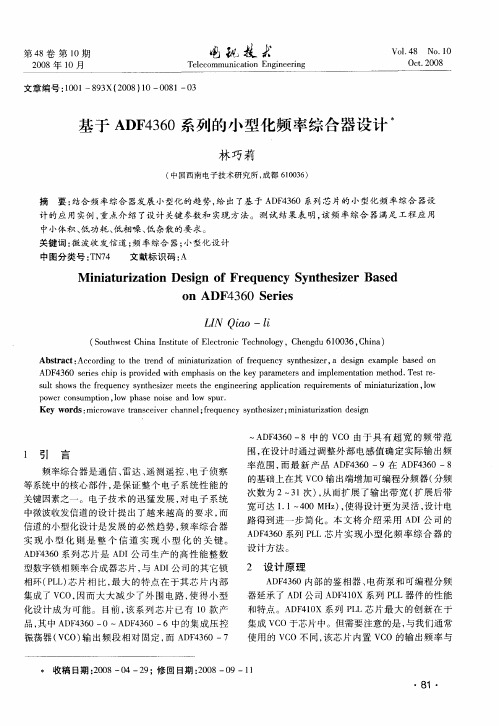
基于ADF4360系列的小型化频率综合器设计
林巧莉
【期刊名称】《电讯技术》
【年(卷),期】2008(48)10
【摘要】结合频率综合器发展小型化的趋势,给出了基于ADF4360系列芯片的小型化频率综合器设计的应用实例,重点介绍了设计关键参数和实现方法.测试结果表明,该频率综合器满足工程应用中小体积、低功耗、低相噪、低杂散的要求.
【总页数】3页(P81-83)
【作者】林巧莉
【作者单位】中国西南电子技术研究所,成都,610036
【正文语种】中文
【中图分类】TN74
【相关文献】
1.堡盟推出新的Clever Level系列小型化设计物位开关 [J], ;
2.一种小型化频率综合器的设计 [J], 白振强;庞建涛;席安安
3.C波段多功能、小型化、低成本频率综合器的设计与实现 [J], 糜光璞
4.频率综合器的小型化设计 [J], 陈强
5.基于MAX10系列FPGA的小型化波控系统的设计与实现 [J], 李化雷;宣浩因版权原因,仅展示原文概要,查看原文内容请购买。
基于ADF4360-1的本振源设计时间:2009-12-16来源:现代电子技术作者:邹玲,石小磊湖北工业大学关键字:4360ADF0 引言在无线通信领域,本振信号性能的优劣是影响混频器输出频谱纯度的主要因素。
频率合成技术是指由一个稳定、准确的标准参考频率,经过一系列的处理过程,产生大量离散的具有同一稳定度和准确度的信号频率。
锁相式频率合成器是一种建立在相位负反馈基础上的闭环控制系统,主要由鉴相器、环路滤波器和压控振荡器组成。
通过锁相频率合成实现的频率源在通信、CATV等领域得到了广泛应用,很多现代电子设备和系统的功能实现都直接依赖于频率源的性能。
ADI公司生产的ADF4360-1是电流型电荷泵数字锁相式频率综合器芯片,具有很高的性价比。
1 ADF4360-1的工作原理及主要性能ADF4360-1主要由数字鉴相器、电荷泵、分频器、计数器及双模前置P/(P+1)分频器等组成。
如图1所示。
1.1 工作原理从ADF4360-1外部输入的信号有标准频率源信号和控制信号,14位可编程参考R分频器对外部频率源信号分频后得到参考频率送至鉴相器。
控制信号由时钟信号CLK、数据信号DATA和使能信号LE组成。
在CLK的控制下,串行输入24位数据信号,暂时存放在24位数据寄存器中。
在接收到使能信号LE后,先前输入的24位数据根据地址位到达对应的锁存器。
ADF4360-1的主分频比N由双模预分频器(P/P+1)、可编程5位A计数器及13位B分频器实现,算法为N=B×P+A,输出频率为:fout=(B×P+A)×fref/R,通过设置A,B,R三个控制字寄存器的控制字来实现对锁相环的控制。
该芯片外围只需添加环路滤波器,根据输出频率大小选择合适的参数,即可输出较稳定的频率。
1.2 主要性能ADF4360-1是美国ADI公司生产的一款高性能锁相频率合成芯片,主要可应用于无线射频通信系统基站(GSM,WCDMA)、手机以及通信检测设备中,为上下变频提供本振信号。