Noise performance of single-electron depressing synapses for neuronal synchrony detection
- 格式:pdf
- 大小:464.86 KB
- 文档页数:6

练习1I、在下列每个句子的空白处填上适当的冠词(如果必要的话),然后将句子译成汉语:1. There has been __an___ ever greater interest in this subject.2. The power rating is the maximum power the resistor can safely dissipate without too great __a_ rise in temperature.3. Its primary disadvantage is __an___ increase in noise.4. __The___ successful design of the equipment requires ___a__ detailed knowledge of the performance specifications.5. In __the___ Bohr model of the hydrogen atom, ___a__ single electron revolves around ___a__ single proton in a circle of radius R.6. The unit of frequency is ___the__ hertz.7. If __a___ voltage is applied across ___a__ circuit, ___an__ electric current will flow in __the___ circuit.8. ____ Fig. 5-1 shows _____ Oersted’s experiment.9. We should use ___an__ 18-volt battery here.10. ___A__ machine is __a___ device for transmitting force to accomplish ___a__ definite purpose.11. ___The__ hydraulic press will be considered in _____ Chapter 14.12.___The__ study of fluids in motion is one of _ the____ more difficult branches of mechanics because of __the___ diversity of phenomena that may occur.13. It is easy to determine __the___ value of __the___ parameter μ.14. By _____ Eq. (2-1) we have _the____ following relation.15. It is necessay to use __an___ S-shaped tube here.16. The authors work at __the___ University of Texas at _____ Arlinton.17. This is __an___ R-bit transformer.18. ___An__ XOR gate must be used here.II、将下列句子译成英语,注意正确地使用冠词:1、这是一个h参数(parameter)。

AAbrupt junction 突变结Accelerated testing 加速实验Acceptor 受主Acceptor atom 受主原子Accumulation 积累、堆积Accumulating contact 积累接触Accumulation region 积累区Accumulation layer 积累层Active region 有源区Active component 有源元Active device 有源器件Activation 激活Activation energy 激活能Active region 有源(放大)区Admittance 导纳Allowed band 允带Alloy-junction device合金结器件Aluminum(Aluminium)铝Aluminum - oxide 铝氧化物Aluminum passivation 铝钝化Ambipolar 双极的Ambient temperature 环境温度Amorphous 无定形的,非晶体的Amplifier 功放扩音器放大器Analogue(Analog)comparator 模拟比较器Angstrom 埃Anneal 退火Anisotropic 各向异性的Anode 阳极Arsenic (AS)砷Auger 俄歇Auger process 俄歇过程Avalanche 雪崩Avalanche breakdown 雪崩击穿Avalanche excitation雪崩激发BBackground carrier 本底载流子Background doping 本底掺杂Backward 反向Backward bias 反向偏置Ballasting resistor 整流电阻Ball bond 球形键合Band 能带Band gap 能带间隙Barrier 势垒Barrier layer 势垒层Barrier width 势垒宽度Base 基极Base contact 基区接触Base stretching 基区扩展效应Base transit time 基区渡越时间Base transport efficiency基区输运系数Base-width modulation基区宽度调制Basis vector 基矢Bias 偏置Bilateral switch 双向开关Binary code 二进制代码Binary compound semiconductor 二元化合物半导体Bipolar 双极性的Bipolar Junction Transistor (BJT)双极晶体管Bloch 布洛赫Blocking band 阻挡能带Blocking contact 阻挡接触Body - centered 体心立方Body-centred cubic structure 体立心结构Boltzmann 波尔兹曼Bond 键、键合Bonding electron 价电子Bonding pad 键合点Bootstrap circuit 自举电路Bootstrapped emitter follower 自举射极跟随器Boron 硼Borosilicate glass 硼硅玻璃Boundary condition 边界条件Bound electron 束缚电子Breadboard 模拟板、实验板Break down 击穿Break over 转折Brillouin 布里渊Brillouin zone 布里渊区Built-in 内建的Build-in electric field 内建电场Bulk 体/体内Bulk absorption 体吸收Bulk generation 体产生Bulk recombination 体复合Burn - in 老化Burn out 烧毁Buried channel 埋沟Buried diffusion region 隐埋扩散区CCan 外壳Capacitance 电容Capture cross section 俘获截面Capture carrier 俘获载流子Carrier 载流子、载波Carry bit 进位位Carry-in bit 进位输入Carry-out bit 进位输出Cascade 级联Case 管壳Cathode 阴极Center 中心Ceramic 陶瓷(的)Channel 沟道Channel breakdown 沟道击穿Channel current 沟道电流Channel doping 沟道掺杂Channel shortening 沟道缩短Channel width 沟道宽度Characteristic impedance 特征阻抗Charge 电荷、充电Charge-compensation effects 电荷补偿效应Charge conservation 电荷守恒Charge neutrality condition 电中性条件Charge drive/exchange/sharing/transfer/storage 电荷驱动/交换/共享/转移/存储Chemmical etching 化学腐蚀法Chemically-Polish 化学抛光Chemmically-Mechanically Polish (CMP)化学机械抛光Chip 芯片Chip yield 芯片成品率Clamped 箝位Clamping diode 箝位二极管Cleavage plane 解理面Clock rate 时钟频率Clock generator 时钟发生器Clock flip-flop 时钟触发器Close-packed structure 密堆积结构Close-loop gain 闭环增益Collector 集电极Collision 碰撞Compensated OP-AMP 补偿运放Common-base/collector/emitter connection 共基极/集电极/发射极连接Common-gate/drain/source connection 共栅/漏/源连接Common-mode gain 共模增益Common-mode input 共模输入Common-mode rejection ratio (CMRR)共模抑制比Compatibility 兼容性Compensation 补偿Compensated impurities 补偿杂质Compensated semiconductor 补偿半导体Complementary Darlington circuit 互补达林顿电路Complementary Metal-Oxide-Semiconductor Field-Effect-Transistor(CMOS)互补金属氧化物半导体场效应晶体管Complementary error function 余误差函数Computer-aided design (CAD)/test(CAT)/manufacture(CAM)计算机辅助设计/ 测试/制造Compound Semiconductor 化合物半导体Conductance 电导Conduction band (edge)导带(底)Conduction level/state 导带态Conductor 导体Conductivity 电导率Configuration 组态Conlomb 库仑Conpled Configuration Devices 结构组态Constants 物理常数Constant energy surface 等能面Constant-source diffusion恒定源扩散Contact 接触Contamination 治污Continuity equation 连续性方程Contact hole 接触孔Contact potential 接触电势Continuity condition 连续性条件Contra doping 反掺杂Controlled 受控的Converter 转换器Conveyer 传输器Copper interconnection system 铜互连系统Couping 耦合Covalent 共阶的Crossover 跨交Critical 临界的Crossunder 穿交Crucible坩埚Crystal defect/face/orientation/lattice 晶体缺陷/晶面/晶向/晶格Current density 电流密度Curvature 曲率Cut off 截止Current drift/dirve/sharing 电流漂移/驱动/共享Current Sense 电流取样Curvature 弯曲Custom integrated circuit 定制集成电路Cylindrical 柱面的Czochralshicrystal 直立单晶Czochralski technique 切克劳斯基技术(Cz法直拉晶体J)DDangling bonds 悬挂键Dark current 暗电流Dead time 空载时间Debye length 德拜长度De.broglie 德布洛意Decderate 减速Decibel (dB)分贝Decode 译码Deep acceptor level 深受主能级Deep donor level 深施主能级Deep impurity level 深度杂质能级Deep trap 深陷阱Defeat 缺陷Degenerate semiconductor 简并半导体Degeneracy 简并度Degradation 退化Degree Celsius(centigrade)/Kelvin 摄氏/开氏温度Delay 延迟Density 密度Density of states 态密度Depletion 耗尽Depletion approximation 耗尽近似Depletion contact 耗尽接触Depletion depth 耗尽深度Depletion effect 耗尽效应Depletion layer 耗尽层Depletion MOS 耗尽MOSDepletion region 耗尽区Deposited film 淀积薄膜Deposition process 淀积工艺Design rules 设计规则Die 芯片(复数dice)Diode 二极管Dielectric 介电的Dielectric isolation 介质隔离Difference-mode input 差模输入Differential amplifier 差分放大器Differential capacitance 微分电容Diffused junction 扩散结Diffusion 扩散Diffusion coefficient 扩散系数Diffusion constant 扩散常数Diffusivity 扩散率Diffusion capacitance/barrier/current/furnace 扩散电容/势垒/电流/炉Digital circuit 数字电路Dipole domain 偶极畴Dipole layer 偶极层Direct-coupling 直接耦合Direct-gap semiconductor 直接带隙半导体Direct transition 直接跃迁Discharge 放电Discrete component 分立元件Dissipation 耗散Distribution 分布Distributed capacitance 分布电容Distributed model 分布模型Displacement 位移Dislocation 位错Domain 畴Donor 施主Donor exhaustion 施主耗尽Dopant 掺杂剂Doped semiconductor 掺杂半导体Doping concentration 掺杂浓度Double-diffusive MOS(DMOS)双扩散MOS.Drift 漂移Drift field 漂移电场Drift mobility 迁移率Dry etching 干法腐蚀Dry/wet oxidation 干/湿法氧化Dose 剂量Duty cycle 工作周期Dual-in-line package (DIP)双列直插式封装Dynamics 动态Dynamic characteristics 动态属性Dynamic impedance 动态阻抗EEarly effect 厄利效应Early failure 早期失效Effective mass 有效质量Einstein relation(ship)爱因斯坦关系Electric Erase Programmable Read Only Memory(E2PROM)一次性电可擦除只读存储器Electrode 电极Electrominggratim 电迁移Electron affinity 电子亲和势Electronic -grade 电子能Electron-beam photo-resist exposure 光致抗蚀剂的电子束曝光Electron gas 电子气Electron-grade water 电子级纯水Electron trapping center 电子俘获中心Electron Volt (eV)电子伏Electrostatic 静电的Element 元素/元件/配件Elemental semiconductor 元素半导体Ellipse 椭圆Ellipsoid 椭球Emitter 发射极Emitter-coupled logic 发射极耦合逻辑Emitter-coupled pair 发射极耦合对Emitter follower 射随器Empty band 空带Emitter crowding effect 发射极集边(拥挤)效应Endurance test =life test 寿命测试Energy state 能态Energy momentum diagram 能量-动量(E-K)图Enhancement mode 增强型模式Enhancement MOS 增强性MOS Entefic (低)共溶的Environmental test 环境测试Epitaxial 外延的Epitaxial layer 外延层Epitaxial slice 外延片Expitaxy 外延Equivalent curcuit 等效电路Equilibrium majority /minority carriers 平衡多数/少数载流子Erasable Programmable ROM (EPROM)可搽取(编程)存储器Error function complement (erfc)余误差函数Etch 刻蚀Etchant 刻蚀剂Etching mask 抗蚀剂掩模Excess carrier 过剩载流子Excitation energy 激发能Excited state 激发态Exciton 激子Extrapolation 外推法Extrinsic 非本征的Extrinsic semiconductor 杂质半导体FFace - centered 面心立方Fall time 下降时间Fan-in 扇入Fan-out 扇出Fast recovery 快恢复Fast surface states 快界面态Feedback 反馈Fermi level 费米能级Fermi-Dirac Distribution 费米-狄拉克分布Femi potential 费米势Fick equation 菲克方程(扩散)Field effect transistor 场效应晶体管Field oxide 场氧化层Filled band 满带Film 薄膜Flash memory 闪烁存储器Flat band 平带Flat pack 扁平封装Flicker noise 闪烁(变)噪声Flip-flop toggle 触发器翻转Floating gate 浮栅Fluoride etch 氟化氢刻蚀Forbidden band 禁带Forward bias 正向偏置Forward blocking /conducting正向阻断/导通Frequency deviation noise频率漂移噪声Frequency response 频率响应Function 函数GGain 增益Gallium-Arsenide(GaAs)砷化钾Gamy ray r 射线Gate 门、栅、控制极Gate oxide 栅氧化层Gauss(ian)高斯Gaussian distribution profile 高斯掺杂分布Generation-recombination 产生-复合Geometries 几何尺寸Germanium(Ge)锗Graded 缓变的Graded (gradual)channel 缓变沟道Graded junction 缓变结Grain 晶粒Gradient 梯度Grown junction 生长结Guard ring 保护环Gummel-Poom model 葛谋-潘模型Gunn - effect 狄氏效应HHardened device 辐射加固器件Heat of formation 形成热Heat sink 散热器、热沉Heavy/light hole band 重/轻空穴带Heavy saturation 重掺杂Hell - effect 霍尔效应Heterojunction 异质结Heterojunction structure 异质结结构Heterojunction Bipolar Transistor(HBT)异质结双极型晶体High field property 高场特性High-performance MOS.(H-MOS)高性能MOS. Hormalized 归一化Horizontal epitaxial reactor 卧式外延反应器Hot carrior 热载流子Hybrid integration 混合集成IImage - force 镜象力Impact ionization 碰撞电离Impedance 阻抗Imperfect structure 不完整结构Implantation dose 注入剂量Implanted ion 注入离子Impurity 杂质Impurity scattering 杂质散射Incremental resistance 电阻增量(微分电阻)In-contact mask 接触式掩模Indium tin oxide (ITO)铟锡氧化物Induced channel 感应沟道Infrared 红外的Injection 注入Input offset voltage 输入失调电压Insulator 绝缘体Insulated Gate FET(IGFET)绝缘栅FET Integrated injection logic集成注入逻辑Integration 集成、积分Interconnection 互连Interconnection time delay 互连延时Interdigitated structure 交互式结构Interface 界面Interference 干涉International system of unions国际单位制Internally scattering 谷间散射Interpolation 内插法Intrinsic 本征的Intrinsic semiconductor 本征半导体Inverse operation 反向工作Inversion 反型Inverter 倒相器Ion 离子Ion beam 离子束Ion etching 离子刻蚀Ion implantation 离子注入Ionization 电离Ionization energy 电离能Irradiation 辐照Isolation land 隔离岛Isotropic 各向同性JJunction FET(JFET)结型场效应管Junction isolation 结隔离Junction spacing 结间距Junction side-wall 结侧壁LLatch up 闭锁Lateral 横向的Lattice 晶格Layout 版图Lattice binding/cell/constant/defect/distortion 晶格结合力/晶胞/晶格/晶格常熟/晶格缺陷/晶格畸变Leakage current (泄)漏电流Level shifting 电平移动Life time 寿命linearity 线性度Linked bond 共价键Liquid Nitrogen 液氮Liquid-phase epitaxial growth technique 液相外延生长技术Lithography 光刻Light Emitting Diode(LED)发光二极管Load line or Variable 负载线Locating and Wiring 布局布线Longitudinal 纵向的Logic swing 逻辑摆幅Lorentz 洛沦兹Lumped model 集总模型MMajority carrier 多数载流子Mask 掩膜板,光刻板Mask level 掩模序号Mask set 掩模组Mass - action law质量守恒定律Master-slave D flip-flop主从D触发器Matching 匹配Maxwell 麦克斯韦Mean free path 平均自由程Meandered emitter junction梳状发射极结Mean time before failure (MTBF)平均工作时间Megeto - resistance 磁阻Mesa 台面MESFET-Metal Semiconductor金属半导体FETMetallization 金属化Microelectronic technique 微电子技术Microelectronics 微电子学Millen indices 密勒指数Minority carrier 少数载流子Misfit 失配Mismatching 失配Mobile ions 可动离子Mobility 迁移率Module 模块Modulate 调制Molecular crystal分子晶体Monolithic IC 单片IC MOSFET金属氧化物半导体场效应晶体管Mos. Transistor(MOST )MOS. 晶体管Multiplication 倍增Modulator 调制Multi-chip IC 多芯片ICMulti-chip module(MCM)多芯片模块Multiplication coefficient倍增因子NNaked chip 未封装的芯片(裸片)Negative feedback 负反馈Negative resistance 负阻Nesting 套刻Negative-temperature-coefficient 负温度系数Noise margin 噪声容限Nonequilibrium 非平衡Nonrolatile 非挥发(易失)性Normally off/on 常闭/开Numerical analysis 数值分析OOccupied band 满带Officienay 功率Offset 偏移、失调On standby 待命状态Ohmic contact 欧姆接触Open circuit 开路Operating point 工作点Operating bias 工作偏置Operational amplifier (OPAMP)运算放大器Optical photon =photon 光子Optical quenching光猝灭Optical transition 光跃迁Optical-coupled isolator光耦合隔离器Organic semiconductor有机半导体Orientation 晶向、定向Outline 外形Out-of-contact mask非接触式掩模Output characteristic 输出特性Output voltage swing 输出电压摆幅Overcompensation 过补偿Over-current protection 过流保护Over shoot 过冲Over-voltage protection 过压保护Overlap 交迭Overload 过载Oscillator 振荡器Oxide 氧化物Oxidation 氧化Oxide passivation 氧化层钝化PPackage 封装Pad 压焊点Parameter 参数Parasitic effect 寄生效应Parasitic oscillation 寄生振荡Passination 钝化Passive component 无源元件Passive device 无源器件Passive surface 钝化界面Parasitic transistor 寄生晶体管Peak-point voltage 峰点电压Peak voltage 峰值电压Permanent-storage circuit 永久存储电路Period 周期Periodic table 周期表Permeable - base 可渗透基区Phase-lock loop 锁相环Phase drift 相移Phonon spectra 声子谱Photo conduction 光电导Photo diode 光电二极管Photoelectric cell 光电池Photoelectric effect 光电效应Photoenic devices 光子器件Photolithographic process 光刻工艺(photo)resist (光敏)抗腐蚀剂Pin 管脚Pinch off 夹断Pinning of Fermi level 费米能级的钉扎(效应)Planar process 平面工艺Planar transistor 平面晶体管Plasma 等离子体Plezoelectric effect 压电效应Poisson equation 泊松方程Point contact 点接触Polarity 极性Polycrystal 多晶Polymer semiconductor聚合物半导体Poly-silicon 多晶硅Potential (电)势Potential barrier 势垒Potential well 势阱Power dissipation 功耗Power transistor 功率晶体管Preamplifier 前置放大器Primary flat 主平面Principal axes 主轴Print-circuit board(PCB)印制电路板Probability 几率Probe 探针Process 工艺Propagation delay 传输延时Pseudopotential method 膺势发Punch through 穿通Pulse triggering/modulating 脉冲触发/调制Pulse Widen Modulator(PWM)脉冲宽度调制punchthrough 穿通Push-pull stage 推挽级QQuality factor 品质因子Quantization 量子化Quantum 量子Quantum efficiency量子效应Quantum mechanics 量子力学Quasi - Fermi-level准费米能级Quartz 石英RRadiation conductivity 辐射电导率Radiation damage 辐射损伤Radiation flux density 辐射通量密度Radiation hardening 辐射加固Radiation protection 辐射保护Radiative - recombination辐照复合Radioactive 放射性Reach through 穿通Reactive sputtering source 反应溅射源Read diode 里德二极管Recombination 复合Recovery diode 恢复二极管Reciprocal lattice 倒核子Recovery time 恢复时间Rectifier 整流器(管)Rectifying contact 整流接触Reference 基准点基准参考点Refractive index 折射率Register 寄存器Registration 对准Regulate 控制调整Relaxation lifetime 驰豫时间Reliability 可*性Resonance 谐振Resistance 电阻Resistor 电阻器Resistivity 电阻率Regulator 稳压管(器)Relaxation 驰豫Resonant frequency共射频率Response time 响应时间Reverse 反向的Reverse bias 反向偏置SSampling circuit 取样电路Sapphire 蓝宝石(Al2O3)Satellite valley 卫星谷Saturated current range电流饱和区Saturation region 饱和区Saturation 饱和的Scaled down 按比例缩小Scattering 散射Schockley diode 肖克莱二极管Schottky 肖特基Schottky barrier 肖特基势垒Schottky contact 肖特基接触Schrodingen 薛定厄Scribing grid 划片格Secondary flat 次平面Seed crystal 籽晶Segregation 分凝Selectivity 选择性Self aligned 自对准的Self diffusion 自扩散Semiconductor 半导体Semiconductor-controlled rectifier 可控硅Sendsitivity 灵敏度Serial 串行/串联Series inductance 串联电感Settle time 建立时间Sheet resistance 薄层电阻Shield 屏蔽Short circuit 短路Shot noise 散粒噪声Shunt 分流Sidewall capacitance 边墙电容Signal 信号Silica glass 石英玻璃Silicon 硅Silicon carbide 碳化硅Silicon dioxide (SiO2)二氧化硅Silicon Nitride(Si3N4)氮化硅Silicon On Insulator 绝缘硅Siliver whiskers 银须Simple cubic 简立方Single crystal 单晶Sink 沉Skin effect 趋肤效应Snap time 急变时间Sneak path 潜行通路Sulethreshold 亚阈的Solar battery/cell 太阳能电池Solid circuit 固体电路Solid Solubility 固溶度Sonband 子带Source 源极Source follower 源随器Space charge 空间电荷Specific heat(PT)热Speed-power product 速度功耗乘积Spherical 球面的Spin 自旋Split 分裂Spontaneous emission 自发发射Spreading resistance扩展电阻Sputter 溅射Stacking fault 层错Static characteristic 静态特性Stimulated emission 受激发射Stimulated recombination 受激复合Storage time 存储时间Stress 应力Straggle 偏差Sublimation 升华Substrate 衬底Substitutional 替位式的Superlattice 超晶格Supply 电源Surface 表面Surge capacity 浪涌能力Subscript 下标Switching time 开关时间Switch 开关TTailing 扩展Terminal 终端Tensor 张量Tensorial 张量的Thermal activation 热激发Thermal conductivity 热导率Thermal equilibrium 热平衡Thermal Oxidation 热氧化Thermal resistance 热阻Thermal sink 热沉Thermal velocity 热运动Thermoelectricpovoer 温差电动势率Thick-film technique 厚膜技术Thin-film hybrid IC薄膜混合集成电路Thin-Film Transistor(TFT)薄膜晶体Threshlod 阈值Thyistor 晶闸管Transconductance 跨导Transfer characteristic 转移特性Transfer electron 转移电子Transfer function 传输函数Transient 瞬态的Transistor aging(stress)晶体管老化Transit time 渡越时间Transition 跃迁Transition-metal silica 过度金属硅化物Transition probability 跃迁几率Transition region 过渡区Transport 输运Transverse 横向的Trap 陷阱Trapping 俘获Trapped charge 陷阱电荷Triangle generator 三角波发生器Triboelectricity 摩擦电Trigger 触发Trim 调配调整Triple diffusion 三重扩散Truth table 真值表Tolerahce 容差Tunnel(ing)隧道(穿)Tunnel current 隧道电流Turn over 转折Turn - off time 关断时间UUltraviolet 紫外的Unijunction 单结的Unipolar 单极的Unit cell 原(元)胞Unity-gain frequency 单位增益频率Unilateral-switch单向开关VVacancy 空位Vacuum 真空Valence(value)band 价带Value band edge 价带顶Valence bond 价键Vapour phase 汽相Varactor 变容管Varistor 变阻器Vibration 振动Voltage 电压WWafer 晶片Wave equation 波动方程Wave guide 波导Wave number 波数Wave-particle duality 波粒二相性Wear-out 烧毁Wire routing 布线Work function 功函数Worst-case device 最坏情况器件Yield 成品率Zener breakdown 齐纳击穿。

Noise Before we study the RF circuit, we will introduce some important parameters. One of them is noise.The radio channel is free space. Random processes are an integral part of communications.If an ideal signal is binary signal shown in this figure , which is corrupted by noise, the final signal can be represented like in that figure.Noise can be defined as the random fluctuation of electrical power that interferes with the desired signal and inhibit communication.. It is usually random and varied. It cannot be avoided completely, but its effects can be reduced by various means, such as reducing the signal bandwidth, increasing the transmitter power, and using low noise amplifiers for weak signals.Noise in communication systems originates both in the channel and in the communication equipment. There are many possible sources of noise. It is helpful to divide noise into two types: external noise which is a property of the channel and internal noise which originated within the communication equipment.In this class, we will focus on the internal noise.Both passive components (resistor) and active devices (diode, transistor, tube ) can be the noise source. These noises are produced by the random motion of eletrons. These noises can be expressed by fluctuation noise.Noises arising in electron tubes, semiconductor diodes, bipolar transistors, or field effect transistors come from a variety of mechanisms.For diodes, a random emission of electrons and holes produces noise,In a bipolar transistor, there is in addition partition noise. This represents the fluctuation in the path that charge carriers take between the base and the collector after leaving the emitter. There is in addition 1/f , or flicker noise that is caused by surface recombination of base minority carrier at the base-emitter junction.Noise parameters1. Voltage average of fluctuation noisedt t v T v Tn T n )(1lim0⎰∞→-=2. Root mean square value (RMS)--∞→-=-=∆⎰2202])([1)(n T n n T nv dt v t v T Lim t vdt t v T Lim t v T n T n)(1)(022⎰∞→-=1. Resistance thermal noiseThe fluctuation noise of resistor is caused by the random motion of electrons in a conductor due to heat.It might seem that we could transmit at any level of signal power and simply introduce a suitable amount of amplification at the receiver end. Unfortunately, this is not the case due to the fact that the signal will be competing with an ever present environment of random signals or noise.(f s fSo the noise power available from a conductor is a function of its temperature:n T f kT N ∆=T N =noise power in wattsk =Boltzmann ‘s constant , 231038.1-⨯ joules/Kelvin(J/K)T =absolute temperature in kelvins (K) ;this can be found by adding 273 to the celciustemperature.n f ∆=noise power bandwidth in Hertz.Noise VoltageOften we are more interested in the noise voltage than in the power involved.R v P 2=Rv P 2=R v P 2=-2nv N R LRThe noise voltage in a circuit must depend on the resistances involved.Fig 1 shows a resistor N R that serves as a noise source connected across another resistorL R which is a load. The noise voltage is represented as a voltage source -2nv in series with anoiseless resistance N R .Assumed a matched load,one-half the noise voltage appear across the road, and the rest is across the resistor that generates the noise.R f kT R N vv n T n n ∆===4)2(22 For example, a simple resistor will create a noise voltage n v due to the random thermal motion of its electrons and this can be shown to have an rms voltage that satisfiesf kTR v n ∆=-42Where T (in Kelvin) is the absolute temperature, f ∆ (in hertz)is the bandwidth of the measurement, R(in ohms) is the resistance and k is the Boltzmann constant. Z providing R isinterpreted as the resistive part of the impedance. From a modeling viewpoint, the noise source can be regarded as an ideal voltage source of magnitude n v in series with a noise free impedance. Alternatively ,It can be regarded as an ideal current source of magnitude n i in parallel with the impedance (f kTG in∆=-42).RG 1=This equation is based on the assumption that power transfer is maximum. That is the source (the resistance generating the noise) and the load (the amplifier or other device that receives the noise0 are assumed to be matched in impedance._2n v _2nI R G RLosslessy reactance can not product thermal noise. In the resonance circuit, the noise is produced by lossy resistance.3. equivalent noise bandwidthIf the noise power density is )(f S⎰=21)(f f df f S P2)()()(f A f S f S i o =The equivalent noise bandwidth is calculated by the noise power equal. It depends on the rectangular area. The width is n f ∆, the height is )(o o f SIt is equal to the area of )(f S o that the width is n f ∆n f ∆ is equivalent bandwidthdf f A f S df f A f S v i i n222)()()()(⎰⎰∞+∞+-==)()(022f A df f A B L ⎰+∞=)(f A : power transmission function 0f : frequency in the middleFor series circuits or parallel circuits, It can be found by taking the square root of the sum of the squares root of the individual voltages or currentsMathematically, we can say, for voltage source in series+++=232221N N N Nt V V V VAnd similarly, for current sources in parallel+++=232221N N N Nt I I I I)(f S o nf ∆When a circuit contains several resistors, the total noise power can be calculated by suitable combination of the resistors . Two resistors in series each produce a mean-squared voltage. Since the individual noise voltage sources are uncorrelated ,the total mean-squared voltage is the sum of the mean-squared voltage of each of the two resistors .Similarly two conductance in parallel each produce a mean-squared noise current that may be added when the two conductances are combined, since the noise currents are uncorrelated.It should be emphasized that two noise voltage cannot be added together ,only the mean-squared values can be added.2. Antenna thermal noiseEquivalent circuit consists of radiation resistance A R and reactance A X .Radiation resistance represents the power of antenna receiving or radiation signaling.n A A n f R kT V ∆=-423. Transistor noiseThe main noises in the transistor include thermal noise , shot noise, distribution noise, flicker noise. The thermal and shot noise are white noises, the others are color noise.3.1 Thermal noiseThermal noise always exists in the base resistance 'bb r .The emitter and collector have seldom resistance.3.2 Shot noiseShot noise is due to random variations in DC current flow in active devices such as tubes, transistors, and semiconductor diodes. These variations are caused by the fact that current is a flow of carrier (electrons or holes), each of which carries a finite amount of charge. Current can thus be considered as a series of pulses, each consisting of the charge carried by one electron. The name “shot noise ” describes the random arrival of electrons arriving at the anode of a vacuum tube, like individual pellets of shot form a shotgunIn the bipolar transistor , the carrier charges that are injected into the base level can injected to the collector and emitter. It can be represented by the current fluctuation of emitter current. Shot noise is usually represented by a current source.Shot noise arise from random variations of a DC current ,0I and is especially associated with current carrying active devices. Shot noise is most apparent in a current source with zero-shunt source admittance.Then the DC current istqn I ∆=q is the charge of an electron shot noise powerf qRI N s ∆=02The corresponding shot noise current :f qI i ∆=-022It is a Gaussian white process. The noise current is given by the equation:f qI qI i o n∆==-222Whereq =magnitude of the charge on an electron, equal to 19106.1-⨯coulombI =average current0I =DC bias current in the devicef ∆= bandwidth over which the noise is observed ,in hertz Shot noise has random amplitude and flat spectrum.em bb b e b e cb c r g r r r r r r 0'0'')1(αα==-==n b bnf kTr v∆=-42n E enf qI i ∆=-223.3 partition noise (distribution noise)It occurs only in devices where a single current separated into two or more paths. An example of such a device is a dipolar junction transistor , where the emitter current is the sum of the collector and base currents. As the charge carriers divided into one stream or the other, a random element in the current is producedn C cnf qI I∆-=•-)1(2022ααaf jf /10+=•ααstate base common of t coefficien amplifier current is α3.4 flicker noise (f1) The noise power varies inversely with frequency. There is proportionately more energy at the low-frequency end of the spectrum than with white noise. It can have some influences in the low frequency. Its frequency spectrum is inversed proportion to the frequency. It is found in tubes but is a more serious problem in semiconductors and in carbon resistors. It is not fully understood, but it is believed to be caused by variations in carrier density.fWLC K V OX n 12=-K: process-dependent constantIn the base level, noise is thermal noise , In the emitter, is shot noise, in the collector is distribution noise.bc --2cn ir12Fnf4 Diode noiseFor diode, we only consider the shot noise. It has not distribution noise and thermal noise is very small.5 field effect transmitterThere are four kinds of noise 1) shot noise in the gate leveln G ngf qI i∆=-222) Channel resistance thermal noise_2ngn f ndf kTg is ∆=-42n f n f g kT V s∆=-)1(4213) Equivalent resistance noise between source and gate leveln n f kTR V∆=-4224) flicker noise (f1) The noise power varies inversely with frequency. There is proportionately more energy at the low-frequency end of the spectrum than with white noise. It can have some influences in the low frequency. Its frequency spectrum is inversed proportion to the frequency. It is found in tubes but is a more serious problem in semiconductors and in carbon resistors. It is not fully understood, but it is believed to be caused by variations in carrier density.fWLC K V OX n 12=-K: process-dependent constantInput-referred noiseThe internal noise of a noisy two port circuit can be modeled by two input noise generators: 1) a serial voltage source -2nv 2) a parallel current source -2n i 3)a noiseless circuit_2v-2nv : an equivalent output noise power to the input by shorting the input port -2ni : an equivalent output noise power to the input by leaving the input portThis is an example:_2nDiiv +-+-:22,2,2,L Dn R n on R iv vL•+=---By shorting the input , and leaving the -2niL m iLi m i o v R g v R v g v v A ===The RMS of output noise voltage --⨯=222,nvon v A v22,22,222,2,22,2)()(mD n L m R n L m LDn R n vo n ngiR g vR g RivAvv LL------+=•+==≈22,mD n gi-BY leaving the input open2222222,))(()(L m i nvi non R g Z i A Z i v---==2222,2,2)(iL m LD n R n nZ R g R ivi L•+=---2222,2)(iL m L Dn nZ R g R ii •=--For )3/2(42m nDg kT i=-)3/(82m ng kT v =- )3/(822i m nZ g kT i =-In general, the noise in an electronic circuit can be modeled by removing the noise sources from within the circuit and replacing them by equivalent current and voltage sources at the input.The main reason for studying and calculating noise power or voltage is the effect that noise has on the desired signal. It is not really the amount of noise that concerns us but rather the amount of noise compared to the level of the desired signal. It is the ratio of signal to noise powerthat is important, rather than the noise power alone.The signal-to noise ratio is one of the most important parameters of any communication system.The SNR is defined as the ratio of the signal power to the total noise power.The crucial quantity in assessing circuit performance is the signal-to-noise ratio (SNR), defined bypowernoise power signal N S SNR ==It is usually expressed in decibels:NSP P dB SNR log10)(= In a radio receiver, SNR will directly relate to the quality of the demodulated signal. The change in SNR through an RF circuit is normally measured in term of its noiseThere is another represent method about noise figurei o i o i o o i S S N N N S N S F //=••=pi oA N N F •=i o p S S A /=pi oA N N F •=p A : the power gain of the amplifierp i o A N N •=1: the output noise power that is the amplified source noise through theamplifier2o N : the noise power of this amplifier 201o o N N N +=.0121N N F o += The average noise figure⎰⎰=dff A df f A f F AV F pp )()()()( Noise figure is occasionally called noise factor. For a noiseless circuit, F=1, This is because both the input signal and the input noise are amplified/attenuated) by the same factor and noadditional noise is introduced.In reality, the finite noise of a system degrades the SNR , yielding F>1.-2-2+-f kTR vS R S∆=--42in SNR is the ratio of the input signal power to the noise generated by the sourceresistance,S R-=22SR inin VV SNR22222])([v sn n R inv out A R i v v v A SNR s----------------++=fkTR R I V VR I V VR I V V F S S n n R S n n R S n n R SSS∆++=++=++=------------------------------------------------4)(1)(1)(222222 v A is a voltage gain from P to out VThe output signal power:222ins in in L vo Z R Z V R A P +=In the output port, the external noise power caused by S R is :222'inS in R L v o Z R Z V R A N S +•=-The noise power of equivalent of input noise:------------------------------+++=22'')(inS in S n in S in n L vo Z R Z R I Z R Z V R A N 2222'''])([inS in S n n R L vooZ R Z R I V V R A N N N S+++=+=---------------])([])([2222222222------------------------------++=++++==S n n R ininS inS n n R L v ins inin L vo o R I V V V Z R Z R I V V R A Z R Z V R A N PSNR SSfkTR A v f kTR A R I V f kTR A f kTR R I V F S v outn S v Sn n s vS S n n ∆=∆++∆=∆++=-------------------------4141])(4[4)(122,2222The noise figure can be calculated by rated power and rated power gain:The rated power is the maximum power of output by source. So the input resistance i R must be matched with the internal resistance s R of the amplifiers i R R =The input rated power isThe input rated noise power isn sns s nni f kT R f kTR R V P ∆=∆==-4442'At the output port , L o R R = output matches.Rated power gain is the power gain that input and output match.ss si R V P 42'=pHn nono so ni si A f kT P P P P P F ∆=='''''// For q : dismatch coefficientq P P ⋅='''''''''//////noso ni si o no o so i ni i si no so ni si P P P P q P q P q P q P P P P P F ===Equivalent noise temperatureIt is another way of specifying the noise performance of a device. It has nothing to do with the actual operating temperature of the circuit. For a linear network, if it produce white noise, we can present this internal noise in the input port, A resistance that have e T temperature will replace the noise., and the network is noiseless. e T is an equivalent noise temperature.The rated input noise power is n e ni f kT P ∆='' ,It is amplified and the output rated noisepower pH ni no A P P '''2=The original noise power n ni f kT P ∆=' ,Its output power :''1ni pH no P A P =T T f kT A kT A P P P P P P P F e n pH e pH no no no no no no no +=∆+=+=+==111'1'2'1'2'1'1' T F T e )1(-=The total output noise is:n e pH no no no f T T A P P P ∆+=+=)('2'1'RRNoise Figure of cascaded stageWhen two or more stages are connected in cascade, as in the receiver, the noise figure of the first stage is the most important in determining the noise performance of the entire system because noise generated in the first stage is amplified in all succeeding stages. Noise produced in later stages is amplified and noise generated in the last stage is amplified least of all.It is possible to derive an equation that relates the total noise figure to the gain and noise figure of each stage.''/siso pH P P A =2o P svThe first stage has a gain 1A and noise figure 1NF , and the second-stage gain and noise figure are 2A and 2NFThe noise power input to the first stage isn i N f kT P ∆=The output power of the first stage is:111pH Ni No A P F P =The output power produced by the first stage amplifier is :11111)1(pH n pH n No n A f kT NF A f kT P P ∆-=∆-=222)1(pH n n A f kT NF P ∆-=Thus the total noise power at the output of the two-stage system is :22212)1(pH n pH No No A f kT NF A P P ∆-+==2No P 22211)1(pH n pH pH Ni A f kT NF A A P NF ∆-+=12121pH n pH No T A NF NF f kT A P NF -+=∆=Friis ’ formula can be generalized to any number of stages:+-+-+-+=3214213121111A A A NF A A NF A NF NF NF TSensitivity and selectivityThe sensitivity of a receiver is normally defined in term of the minimum detectable signal (MDS) that the system can detect with acceptable signal-to-noise ratio.min,min ,/out R in out inSNR P P SNR SNR F S ==))()((min ,min ,min ,out out R in SNR F f KT SNR F P P S ∆=••=)(log 10)()/(|min ,min ,dB SNR f dB F Hz dBm kT dBm P out in +∆++=K T 290=Dynamic rangeDR is generally defined as the ratio of the maximum input level that the circuit can tolerate to the minimum input level at which the circuit provides a reasonable signal quality.)(log 10)()/(174|min ,min ,dB SNR f dB F Hz dBm dBm P out in +∆++-=。

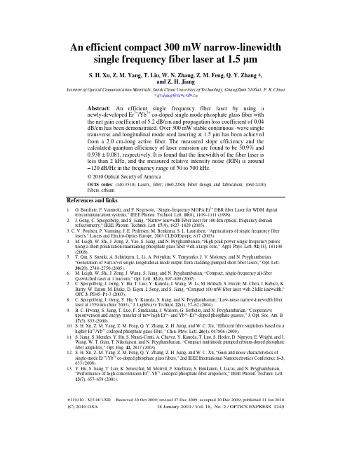
An efficient compact 300 mW narrow-linewidth single frequency fiber laser at 1.5 µmS. H. Xu, Z. M. Yang, T. Liu, W. N. Zhang, Z. M. Feng, Q. Y. Zhang *,and Z. H. JiangInstitute of Optical Communication Materials, South China University of Technology, GuangZhou 510641, P. R. China* qyzhang@Abstract: An efficient single frequency fiber laser by using anewly-developed Er3+/Yb3+ co-doped single mode phosphate glass fiber withthe net gain coefficient of 5.2 dB/cm and propagation loss coefficient of 0.04dB/cm has been demonstrated. Over 300 mW stable continuous -wave singletransverse and longitudinal mode seed lasering at 1.5 µm has been achievedfrom a 2.0 cm-long active fiber. The measured slope efficiency and thecalculated quantum efficiency of laser emission are found to be 30.9% and0.938 ± 0.081, respectively. It is found that the linewidth of the fiber laser isless than 2 kHz, and the measured relative intensity noise (RIN) is around−120 dB/Hz in the frequency range of 50 to 500 kHz.© 2010 Optical Society of AmericaOCIS codes: (140.3510) Lasers, fiber; (060.2280) Fiber design and fabrication; (060.2410)Fibers, erbiumReferences and links1. G. Bonfrate, F. Vaninetti, and F. Negrisolo, “Single-frequency MOPA Er3+ DBR fiber Laser for WDM digitaltelecommunication systems,” IEEE Photon. Technol. Lett. 10(8), 1109–1111 (1998).2. J. Geng, C. Spiegelberg, and S. Jiang, “Narrow linewidth Fiber laser for 100-km optical. frequency domainreflectometry,” IEEE Photon. Technol. Lett. 17(9), 1827–1829 (2005).3. C. V. Poulsen, P. Varming, J. E. Pedersen, M. Beukema, S. L. Lauridsen, “Applications of single frequency fiberlasers,” Lasers and Electro-Optics Europe, 2003 CLEO/Europe, 617 (2003)4. M. Leigh, W. Shi, J. Zong, Z. Yao, S. Jiang, and N. Peyghambarian, “High peak power single frequency pulsesusing a short polarization-maintaining phosphate glass fiber with a large core,” Appl. Phys. Lett. 92(18), 181108 (2008).5. T. Qiu, S. Suzuki, A. Schülzgen, L. Li, A. Polynkin, V. Temyanko, J. V. Moloney, and N. Peyghambarian,“Generation of watt-level single-longitudinal-mode output from cladding-pumped short fiber lasers,” Opt. Lett.30(20), 2748–2750 (2005).6. M. Leigh, W. Shi, J. Zong, J. Wang, S. Jiang, and N. Peyghambarian, “Compact, single-frequency all-fiberQ-switched laser at 1 microm,” Opt. Lett. 32(8), 897–899 (2007).7. C. Spiegelberg, J. Geng, Y. Hu, T. Luo, Y. Kaneda, J. Wang, W. Li, M. Brutsch, S. Hocde, M. Chen, J. Babico, K.Barry, W. Eaton, M. Blake, D. Eigen, I. Song, and S. Jiang, “Compact 100 mW fiber laser with 2 kHz linewidth,”OFC 3, PD45–P1-3 (2003).8. C. Spiegelberg, J. Geng, Y. Hu, Y. Kaneda, S. Jiang, and N. Peyghambarian, “Low-noise narrow-linewidth fiberlaser at 1550 nm (June 2003),” J. Lightwave Technol. 22(1), 57–62 (2004).9. B. C. Hwang, S. Jiang, T. Luo, F. Smekatala, J. Watson, G. Sorbello, and N. Peyghambarian, “Cooperativeupconversion and energy transfer of new high Er3+- and Yb3+–Er3+-doped phosphate glasses,” J. Opt. Soc. Am. B 17(5), 833 (2000).10. S. H. Xu, Z. M. Yang, Z. M. Feng, Q. Y. Zhang, Z. H. Jiang, and W. C. Xu, “Efficient fibre smplifiers based on ahighly Er3+/Yb3+ codoped phosphate glass-fibre,” Chin. Phys. Lett. 26(4), 047806 (2009).11. S. Jiang, S. Mendes, Y. Hu, S. Nunzi-Conti, A. Chavez, Y. Kaneda, T. Luo, S. Hodce, D. Nguyen, E. Wright, and J.Wang, W. T. Gian, T. Nikolajsen, and N. Peyghambarian, “Compact multimode pumped erbium-doped phosphate fiber amplifers,” Opt. Eng. 42, 2817 (2003).12. S. H. Xu, Z. M. Yang, Z. M. Feng, Q. Y. Zhang, Z. H. Jiang, and W. C. Xu, “Gain and noise characteristics ofsingle-mode Er3+/Yb3+ co-doped phosphate glass fibers,” 2nd IEEE International Nanoelectronics Conference 1–3, 633 (2008)13. Y. Hu, S. Jiang, T. Luo, K. Seneschal, M. Morrell, F. Smehtala, S. Honkanen, J. Lucas, and N. Peyghambarian,“Performance of high-concentration Er3+-Yb3+-codoped phosphate fiber amplifiers,” IEEE Photon. Technol. Lett.13(7), 657–659 (2001).#119310 - $15.00 USD Received 30 Oct 2009; revised 27 Dec 2009; accepted 30 Dec 2009; published 11 Jan 2010 (C) 2010 OSA18 January 2010 / Vol. 18, No. 2 / OPTICS EXPRESS 124914. C. Jacinto, S. L. Oliveira, T. Catundab, A. Andrade, J. Myers, and M. Myers, “Upconversion effect on fluorescencequantum efficiency and heat generation in Nd3+-doped materials,” Opt. Express 13(6), 2040–2046 (2005).15. M. Karasek, “Optimum design of Er3+-Yb3+ codoped fibers for large-signal high-pump-power applications,” IEEEJ. Quantum Electron. 33(10), 1699–1705 (1997).16. T. Liu, Z. M. Yang, and S. H. Xu, “3-Dimensional heat analysis in short-length Er3+/Yb3+ co-doped phosphate fiberlaser with upconversion,” Opt. Express 17(1), 235–247 (2009).17. W. L. Barnes, P. R. Morkel, L. Reekie, and D. N. Payne, “High-quantum-efficiency Er(3+) fiber lasers pumped at980 nm,” Opt. Lett. 14(18), 1002–1004 (1989).1. IntroductionSingle frequency fiber laser has been the subject of intense research in the last two decades for applications, such as high resolution sensing, coherent telecommunication, optical frequency domain reflectometry, and as a seed laser for LIDAR [1–3]. Of these short resonance cavity configuration, such as distributed Bragg reflector (DBR), is beneficial to single frequency laser emission for mode-hop free, narrower linewidth, lower noise, and all in a compact all- fiber design [4–8]. Recently, Spiegelberg et al have reported DBR laser emission around 1550 nm in Er3+/Yb3+ co-doped phosphate glass fibers [7,8]. Single frequency laser with the output power of over 200 mW and the linewidth of < 2 kHz has been achieved from a 2-cm-length phosphate glass fiber by the authors. However, the effective length of the resonator is designed to be 5 cm, which easily leads to multi-longitude emissions. In order to select one longitudinal mode, the linear cavity should be shortened further or a composite fiber grating should be adopted. Shortening the resonance cavity will limit the laser output power and thus higher concentrations of rare-earth ions should be doped into the glass fiber core. Furthermore, the upconversion effects will be more serious with the increase of the concentrations of rare-earth ions [9], and a great deal of heat generated will decrease the quantum efficiency further. Therefore, developing the Er3+/Yb3+ co-doped phosphate glass fiber with high gain coefficient and low propagation loss and low heat accumulation are key points to achieve efficient single frequency lasers.Recently, we have reported that a homemade 3.0 cm Er3+/Yb3+-codoped phosphate glass fiber could provide an internal gain up to 36 dB [10]. Here we report a more efficient and compact single frequency fiber laser with high output power and narrow linewidth based on our newly-developed Er3+/Yb3+-codoped phosphate single mode glass fibers and the 3D short-cavity heat flow model.2. Active fiber and single frequency fiber laser designRE ions were doped uniformly in the core region with concentrations of 3.0mol% for Er3+, and 5.0mol% for Yb3+, respectively. The fluorescence lifetime of the 4I13/2-4I15/2 transition of Er3+ ions is 8.1 ms in a phosphate fiber 4 mm in length. The absorption and emission cross sections are 5.96 × 10⁻²¹ cm2, and 7.17 × 10⁻²¹ cm2 at 1534 nm, respectively. The refractive index of the core and cladding glass are measured to be 1.535 and 1.522 via a prism coupler (Metricon Model 2010) at 1310 nm, respectively. The phosphate glass fiber designed has a core diameter of 5.4 µm with a numerical aperture (NA) of 0.206 at 1.5 µm. The Er3+/Yb3+-codoped phosphate glass fiber was fabricated using a fiber-drawing tower (TDR-2, Japan) based on the rod-in-tube technique [10]. The cross section of the phosphate glass fiber is detected via an amplified CCD viewer, as shown in the inset of Fig. 1. The core-to-cladding offset is less than 0.4 µm. The mode-field diameter at 1550 nm is estimated to be 6.24 µm and the cut-off wavelength was calculated to be 1470 nm. The average propagation loss measured by the cut-back method is lower than 0.04 dB/cm at 1310nm, which is the lowest value reported in this kind of fiber [7,8,10–13]. The gain and noise figure characteristics of the Er3+/Yb3+-codoped phosphate glass fiber have been demonstrated, as shown in Fig. 1. A net gain per unit length of up to 5.2 dB/cm at 1535 nm was obtained from a 40-mm-length Er3+/Yb3+-codoped phosphate glass fiber, which is the highest gain coefficient reported in this kind of fiber [7,8,10–13]. The obtained noise figures of different signal wavelengths from 1525 nm to 1565 nm were less than 5.5 dB.#119310 - $15.00 USD Received 30 Oct 2009; revised 27 Dec 2009; accepted 30 Dec 2009; published 11 Jan 2010 (C) 2010 OSA18 January 2010 / Vol. 18, No. 2 / OPTICS EXPRESS 12501520153015401550156015700510152025G a i n (d B )Wavelength (nm)N o i s e F i g u r e (d B )Fig. 1. Gain and noise figure characteristics of the Er 3+/Yb 3+ codoped phosphate glass fiber.Inset: the cross section of the phosphate glass fiber. Pump power P p = 330.8 mW,signal input power P in = −30 dBm, fiber length 40 mm.A laser cavity is established by one spectrally narrow band fiber Bragg grating (NB-FBG) and one dielectric mirror that is butt-coupled to the one end facet ofa short piece of Er 3+/Yb 3+-codoped phosphate fiber, as shown in Fig. 2. The NB-FBG with a 3-dB linewidth of 0.06 nm and a center-wavelength reflectivity 50.5% has been fabricated. The reflectivity ofFig. 2. Experimental setup of compact short Er 3+/Yb 3+ co-doped phosphate fiber laser.the dielectric mirror is larger than 99.5% at the signal wavelength of 1535 nm and smaller than 5% at the pump wavelength of 976 nm, which can diminish the pump light back to the pump laser diodes (LDs) and thus reduces the instability of the pump source. In order to improve the pump/signal coupling efficiency further, the NB-FBG had been irradiated in the Corning HI 1060 FLEX fiber with a mode-field diameter of 6.3µm at 1550 nm and 4.0µm at 976 nm. The NB-FBG was fused splicing with the 2-cm long phosphate fiber. The effective length of the resonator includes the 2.0 cm active fiber and a half of the 1.5 cm NB-FBG irradiated area. It is less than 3 cm, giving a longitudinal mode spacing of 3.4 GHz. The NB-FBG has a reflection bandwidth of less than 7.5 GHz, supporting only one longitudinal mode. The laser cavity was assembled into a copper tube, which was temperature-controlled by a cooling system with the resolution of 0.05°C. With a proper temperature control, the laser will operate in a single frequency without mode hop and mode competition phenomena. Two high power 976 nm FBG-stabilized pump lasers (PL1 and PL2) with orthogonal polarization output were combined through a polarization beam combiner (PBC). The pump lasers are coupled into the laser cavity through a 980/1550 nm WDM. The emission spectrum and the optical power of fiber laser is (C) 2010 OSA 18 January 2010 / Vol. 18, No. 2 / OPTICS EXPRESS 1251#119310 - $15.00 USD Received 30 Oct 2009; revised 27 Dec 2009; accepted 30 Dec 2009; published 11 Jan 2010measured by an optical spectrum analyser (OSA, Anritsu MS9710C) and a power meter (PM, Ophir NovaII), respectively.3. Single-frequency fiber laser performanceFigure 3 shows the laser output power at 1.5 µm from the Er 3+/Yb 3+-codoped phosphate glass fiber versus the pump power. The lasing threshold is around 80 mW. When the pump power is above the threshold, the laser output power is linearly enhanced with increasing the pump power. A maximum output power of 306 mW has been achieved from the 2.0 cm phosphate fiber at the pump power of 1072 mW, which is, to the best of our knowledge, the highest output power from this kind of fiber lasers reported to date. [7-12] The slope efficiency of the laser emission is measured to be 30.9% and the experimental quantum efficiency of the laser emission related to the absorbed pump power is estimated to be 58% since only 84% of the pump power is coupled into the phosphate fibre core due to the coupling loss, scattering, and pump leakage. It should be pointed out that the pump power illustrated in Fig. 3 is the nominal power before coupling into the WDM. No output power saturation phenomenon is observed, indicating that the output power will rise further with increasing the pump power. The center wavelength of laser emission spectrum of 1534.75 nm and the side mode suppression ratio (SMSR) of > 65 dB has been measured by the OSA. The transient fluctuations of the output power at 250 mW have been investigated as shown in the inset of Fig. 3. The output power fluctuations of < ± 0.18% of the average power were observed, which is caused by the small fluctuations in the pump laser power. Meanwhile, we have measured the long-term stability of the output power over 40 h. If the ambient temperature is held 23°C, the output power fluctuations were less than ± 0.5% over the entire period of time.02004006008001000 F i b e r L a s e r O u t p u t P o w e r (m W ) Pump Power (mW)Fig. 3. Output power of the single frequency fiber laser versus pump power. Inset: the transientfluctuations of the fiber laser output power.In order to assess the performance of Er 3+/Yb 3+ co-doped glass fiber and intend to further increase the laser output power, it is necessary to evaluate the quantum efficiency φ without and with laser action, the former is fluorescence quantum efficiency and the latter is defined as the fraction of emitted photons by the absorbed photons. Without laser action the fluorescence quantum efficiency (the ratio between its radiative and total rates) is given as φ = τ/τrad [14], and the value is gotten to be ~0.903. The fractional thermal loading η can be determined by the quantum efficiency φ as η = 1−φ (λex / <λem >) and the value is 0.431. With laser emission the quantum efficiency φ in fiber laser can be expressed as [15]:(C) 2010 OSA 18 January 2010 / Vol. 18, No. 2 / OPTICS EXPRESS 1252#119310 - $15.00 USD Received 30 Oct 2009; revised 27 Dec 2009; accepted 30 Dec 2009; published 11 Jan 20101/p s s ah P T h P νϕν= where T 1 is the transmission coefficient of the output coupler. P s is the output power of signal light. νp and νs are the pump and signal frequency, respectively. P a is the fraction of the pump power absorbed which is determined theoretically based on the space-dependent rate equations for the Er 3+ and Yb 3+ population densities [16]. Figure 4 show the quantum efficiency in different pump power above the threshold value. The average quantum efficiency is found to be 0.938 ± 0.081 in our laser system, which is nearly the same as the Er 3+ doped fiber laser reported by Barnes [17]. The results show that an efficient energy-transfer exists in the Er 3+/Yb 3+ codoped phosphate glass fiber.Q u a n t u m E f f i c i e n c y Pump Power (mW)Fig. 4 Quantum efficiency vs pump power above the threshold value.The single frequency operation was verified by a scanning Fabry–Pérot spectrum analyzer that had a free spectral range of 300 MHz and a finesse of 300. In order to further investigate the laser spectral characteristics, the linewidth ofthe fiber laser was measured by the self-homodyne method using a 48.8-km-fiber delay. Figure 5 shows the homodyne signalR F P o w e r (d B m )Frequency (kHz)Fig. 5. The lineshape of the homodyne signal measured with 48.8 km fiber-delay and the laserlinewidth is approximately 1.6 kHz FWHM.spectrum of the fiber laser measured by a radio frequency (RF) electrical spectrum analyzer (ESA, Aglient N9320A). It is 32 kHz with −20 dB from the peak, which indicates the laser linewidth is approximately 1.6 kHz FWHM. The rise at the zero frequency is caused by the RF (C) 2010 OSA 18 January 2010 / Vol. 18, No. 2 / OPTICS EXPRESS 1253#119310 - $15.00 USD Received 30 Oct 2009; revised 27 Dec 2009; accepted 30 Dec 2009; published 11 Jan 2010spectrum analyzer. The fall at low frequencies below 2 kHz is caused by the low-frequency filter in the photoreceiver. 0100200300400500-160-140-120-100-80-60R I N (d B /H z )Frequency (kHz)Fig. 6. The relative intensity noise (RIN) of the fiber laser.The relative intensity noise (RIN) of the fiber laser has been measured and is shown in Fig.6. The RIN at the low frequencies of < 50 kHz decreases from −86 dB/Hz to −120 dB/Hz with increasing the frequency and is stabilized at approximately −120 dB/Hz for frequencies above 50 kHz. The peak of RIN is observed at the several kHz, which is mainly caused by the ambient acoustics and vibration. The peak of the relaxation oscillation frequency of the fiber laser hasn’t been observed at the frequencies of < 500kHz.4. ConclusionsIn summary, we have demonstrated a 300 mW narrow linewidth fiber laser at 1.5 µm from an 2.0-cm short-length Er 3+/Yb 3+ heavily doped phosphate fiber. The fiber laser operates at a single frequency with the linewidth less than 2 kHz and the slope efficiency is 30.9%. The relative intensity noise (RIN) of the fiber laser is found to be −120 dB/Hz for frequencies above 50 kHz. The results indicate that the Er 3+/Yb 3+-codoped phosphate single mode glass fiber might be a promising candidate as an efficient narrow-linewidth single frequency fiber laser.AcknowledgementThe authors would like to acknowledge support from the NSFC (Grant Nos. U0934001 and 60977060).(C) 2010 OSA 18 January 2010 / Vol. 18, No. 2 / OPTICS EXPRESS 1254#119310 - $15.00 USD Received 30 Oct 2009; revised 27 Dec 2009; accepted 30 Dec 2009; published 11 Jan 2010。
电子倍增CCD(EMCCD)性能参数测试摘要:介绍了电子倍增CCD工作原理及噪声特性,并据此设计了电子倍增CCD 的参数测试方法。
通过对电子倍增CCD相机进行测试,并运用Matlab对数据进行分析处理,得到了电子倍增CCD的一些重要的性能参数(包括读出噪声,转换增益,满阱,倍增增益,暗电流以及时钟感生噪声)。
最后,我们分析了参数的正确性。
关键字:电子倍增CCD;噪声特性引言电子倍增CCD(EMCCD)技术,有时也被称作“片上增益”技术,是一种全新的微弱光信号增强探测技术。
自Andor Technology Ltd于2001年首次将其应用在iXon系列高端超高灵敏相机以来,EMCCD技术受到了广泛关注。
EMCCD具有低噪声、高灵敏度、高动态范围等特点,因此在微光夜视中也具有较大优势。
但是在微光成像领域,尤其是探测极微弱目标时,对电子倍增CCD的性能指标要求极其严格,需要获取电子倍增CCD的一些重要性能参数,以此判断该器件是否满足整个成像系统的工作要求。
另外,在研制电子倍增CCD 成像系统的过程中,特别是在调试阶段,需要经常测试有关指标,以此判断系统是否达到预期目标。
本项目研究的电子倍增CCD性能参数测试方法,可广泛应用于微光成像系统测试领域,具有十分重要的实用价值。
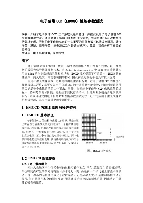
1.EMCCD的基本原理与噪声特性1.1 EMCCD基本原理电子倍增CCD的结构与普通CCD相似,只是在读出寄存器与输出放大器之间增加了一个特殊的倍增寄存器,如右图。
倍增寄存器的结构与读出寄存器类似,但是其中一相电极被一对电极取代,第一个电极加直流电压,第二个电极由高电压时钟驱动。
两个电极间的电势差形成强电场,使转移到该电极下的信号电荷与硅晶格发生碰撞电离,激发出新电子,实现了信号电荷的倍增。
图1.1EMCCD基本结构1.2 EMCCD性能参数1.2.1光子散粒噪音光注入光敏区产生信号电荷的过程可看作独立、均匀、连续发生的随机过程。
单位时间内产生的信号电荷数目并非绝对不变,而是在一个平均值上作微小的波动。
毕业设计(论文)外文文献翻译翻译(1)题目相控阵和雷达技术的突破翻译(2)题目发射KU-波段的相控阵天线在FSS通信系统中的应用学院电子信息学院专业英文译文1:相控阵和雷达技术的突破【摘要】许多人认为雷达是一个成熟的领域,不会发生任何新的变化,这种看法存在很久了,没有比这个看法更错误的了。
当我1950年参与到雷达领域的时候,我也有过同样的看法,例如,我认为麻省理工学院的雷达丛书已经是包罗万象了,不需要增加任何新的内容。
然而我是多么的错啊,从那时起雷达技术领域中已经发生了许多令人眼花缭乱的发展,雷达一直受益于Moore s定律和许多新的技术上的成果,例如,MMIC GaAs T/R组件和相控阵组件。
现在雷达技术发展得更快了,在这篇文章里,我将给出某些最近突破的例子。
【关键词】雷达;有源相控阵;MMIC;MEMS;T/R组件;相控阵;AESA;电扫;GaAs;GaN;SiC;CMOS;数字波束形成;自适应阵列;旁瓣对消器;超宽带天线;金属材料;电子管;真空电子器件;回旋管;磁控管;速调管;行波管;微波功率组件;MPM;功率放大组件;SBX;GBR—P0:SEA-BASED X-波段雷达24层楼高的SEA-BASED X-波段相控阵雷达是一个世界奇迹。
1:GaAs MMIC T/R模块(单片微波集成电路)在过去的十年成功和广泛的应用了MMIC和AESA(有源电子扫描阵)2:低成本¥19K AESA谁说AESA是非常昂贵的,在DARPA(Defense Advanced Research Projects Agency美国国防部先进研究项目局)的低资金¥19K资助下使35GHZ相控阵成为可能。
DARPA 已经资助发展了¥10 X-band,10’smW,单T/R芯片模块。
3:低成本的MEMS(微机电系统)相控阵即使我们只有一个低损耗的移相器,那么就能够用在一个模块上安装很多的移相而MEMS提供了这个可能。
微电子学与固体电子学专业英语词汇Abrupt junction 突变结Accelerated testing 加速实验Acceptor 受主Acceptor atom 受主原子Accumulation 积累、堆积Accumulating contact 积累接触Accumulation region 积累区Accumulation layer 积累层Active region 有源区Active component 有源元Active device 有源器件Activation 激活Activation energy 激活能Active region 有源(放大)区Admittance 导纳Allowed band 允带Alloy-junction device合金结器件Aluminum(Aluminium)铝Aluminum - oxide 铝氧化物Aluminum passivation 铝钝化Ambipolar 双极的Ambient temperature 环境温度Amorphous 无定形的,非晶体的Amplifier 功放扩音器放大器Analogue(Analog)comparator 模拟比较器Angstrom 埃Anneal 退火Anisotropic 各向异性的Anode 阳极Arsenic (AS)砷Auger 俄歇Auger process 俄歇过程Avalanche 雪崩Avalanche breakdown 雪崩击穿Avalanche excitation雪崩激发Background carrier 本底载流子Background doping 本底掺杂Backward 反向Backward bias 反向偏置Ballasting resistor 整流电阻Ball bond 球形键合Band 能带Band gap 能带间隙Barrier 势垒Barrier layer 势垒层Barrier width 势垒宽度Base 基极Base contact 基区接触Base stretching 基区扩展效应Base transit time 基区渡越时间Base transport efficiency基区输运系数Base-width modulation基区宽度调制Basis vector 基矢Bias 偏置Bilateral switch 双向开关Binary code 二进制代码Binary compound semiconductor 二元化合物半导体Bipolar 双极性的Bipolar Junction Transistor (BJT)双极晶体管Bloch 布洛赫Blocking band 阻挡能带Blocking contact 阻挡接触Body - centered 体心立方Body-centred cubic structure 体立心结构Boltzmann 波尔兹曼Bond 键、键合Bonding electron 价电子Bonding pad 键合点Bootstrap circuit 自举电路Bootstrapped emitter follower 自举射极跟随器Boron 硼Borosilicate glass 硼硅玻璃Boundary condition 边界条件Bound electron 束缚电子Breadboard 模拟板、实验板Break down 击穿Break over 转折Brillouin 布里渊Brillouin zone 布里渊区Built-in 内建的Build-in electric field 内建电场Bulk 体/体内Bulk absorption 体吸收Bulk generation 体产生Bulk recombination 体复合Burn - in 老化Burn out 烧毁Buried channel 埋沟Buried diffusion region 隐埋扩散区Can 外壳Capacitance 电容Capture cross section 俘获截面Capture carrier 俘获载流子Carrier 载流子、载波Carry bit 进位位Carry-in bit 进位输入Carry-out bit 进位输出Cascade 级联Case 管壳Cathode 阴极Center 中心Ceramic 陶瓷(的)Channel 沟道Channel breakdown 沟道击穿Channel current 沟道电流Channel doping 沟道掺杂Channel shortening 沟道缩短Channel width 沟道宽度Characteristic impedance 特征阻抗Charge 电荷、充电Charge-compensation effects 电荷补偿效应Charge conservation 电荷守恒Charge neutrality condition 电中性条件Chargedrive/exchange/sharing/transfer/storage 电荷驱动/交换/共享/转移/存储Chemmical etching 化学腐蚀法Chemically-Polish 化学抛光Chemmically-Mechanically Polish (CMP)化学机械抛光Chip 芯片Chip yield 芯片成品率Clamped 箝位Clamping diode 箝位二极管Cleavage plane 解理面Clock rate 时钟频率Clock generator 时钟发生器Clock flip-flop 时钟触发器Close-packed structure 密堆积结构Close-loop gain 闭环增益Collector 集电极Collision 碰撞Compensated OP-AMP 补偿运放Common-base/collector/emitter connection 共基极/集电极/发射极连接Common-gate/drain/source connection 共栅/漏/源连接Common-mode gain 共模增益Common-mode input 共模输入Common-mode rejection ratio (CMRR)共模抑制比Compatibility 兼容性Compensation 补偿Compensated impurities 补偿杂质Compensated semiconductor 补偿半导体Complementary Darlington circuit 互补达林顿电路Complementary Metal-Oxide-Semiconductor Field-Effect-Transistor(CMOS)互补金属氧化物半导体场效应晶体管Complementary error function 余误差函数Computer-aided design (CAD)/test(CAT)/manufacture(CAM)计算机辅助设计/ 测试/制造Compound Semiconductor化合物半导体Conductance 电导Conduction band (edge)导带(底)Conduction level/state 导带态Conductor 导体Conductivity 电导率Configuration 组态Conlomb 库仑Conpled Configuration Devices 结构组态Constants 物理常数Constant energy surface 等能面Constant-source diffusion恒定源扩散Contact 接触Contamination 治污Continuity equation 连续性方程Contact hole 接触孔Contact potential 接触电势Continuity condition 连续性条件Contra doping 反掺杂Controlled 受控的Converter 转换器Conveyer 传输器Copper interconnection system 铜互连系统Couping 耦合Covalent 共阶的Crossover 跨交Critical 临界的Crossunder 穿交Crucible坩埚Crystal defect/face/orientation/lattice 晶体缺陷/晶面/晶向/晶格Current density 电流密度Curvature 曲率Cut off 截止Currentdrift/dirve/sharing 电流漂移/驱动/共享Current Sense 电流取样Curvature 弯曲Custom integrated circuit 定制集成电路Cylindrical 柱面的Czochralshicrystal 直立单晶Czochralski technique 切克劳斯基技术(Cz法直拉晶体J)Dangling bonds 悬挂键Dark current 暗电流Dead time 空载时间Debye length 德拜长度De.broglie 德布洛意Decderate 减速Decibel (dB)分贝Decode 译码Deep acceptor level 深受主能级Deep donor level 深施主能级Deep impurity level 深度杂质能级Deep trap 深陷阱Defeat 缺陷Degenerate semiconductor 简并半导体Degeneracy 简并度Degradation 退化Degree Celsius(centigrade)/Kelvin 摄氏/开氏温度Delay 延迟Density 密度Density of states 态密度Depletion 耗尽Depletion approximation 耗尽近似Depletion contact 耗尽接触Depletion depth 耗尽深度Depletion effect 耗尽效应Depletion layer 耗尽层Depletion MOS 耗尽MOS Depletion region 耗尽区Deposited film 淀积薄膜Deposition process 淀积工艺Design rules 设计规则Die 芯片(复数dice)Diode 二极管Dielectric 介电的Dielectric isolation 介质隔离Difference-mode input 差模输入Differential amplifier 差分放大器Differential capacitance 微分电容Diffused junction 扩散结Diffusion 扩散Diffusion coefficient 扩散系数Diffusion constant 扩散常数Diffusivity 扩散率Diffusion capacitance/barrier/current/furnace 扩散电容/势垒/电流/炉Digital circuit 数字电路Dipole domain 偶极畴Dipole layer 偶极层Direct-coupling 直接耦合Direct-gap semiconductor 直接带隙半导体Direct transition 直接跃迁Discharge 放电Discrete component 分立元件Dissipation 耗散Distribution 分布Distributed capacitance 分布电容Distributed model 分布模型Displacement 位移Dislocation 位错Domain 畴Donor 施主Donor exhaustion 施主耗尽Dopant 掺杂剂Doped semiconductor 掺杂半导体Doping concentration 掺杂浓度Double-diffusive MOS(DMOS)双扩散MOS.Drift 漂移Drift field 漂移电场Drift mobility 迁移率Dry etching 干法腐蚀Dry/wet oxidation 干/湿法氧化Dose 剂量Duty cycle 工作周期Dual-in-line package (DIP)双列直插式封装Dynamics 动态Dynamic characteristics 动态属性Dynamic impedance 动态阻抗Early effect 厄利效应Early failure 早期失效Effective mass 有效质量Einstein relation(ship)爱因斯坦关系Electric Erase Programmable Read Only Memory(E2PROM)一次性电可擦除只读存储器Electrode 电极Electrominggratim 电迁移Electron affinity 电子亲和势Electronic -grade 电子能Electron-beam photo-resist exposure 光致抗蚀剂的电子束曝光Electron gas 电子气Electron-grade water 电子级纯水Electron trapping center 电子俘获中心Electron Volt (eV)电子伏Electrostatic 静电的Element 元素/元件/配件Elemental semiconductor 元素半导体Ellipse 椭圆Ellipsoid 椭球Emitter 发射极Emitter-coupled logic 发射极耦合逻辑Emitter-coupled pair 发射极耦合对Emitter follower 射随器Empty band 空带Emitter crowding effect 发射极集边(拥挤)效应Endurance test =life test 寿命测试Energy state 能态Energy momentum diagram 能量-动量(E-K)图Enhancement mode 增强型模式Enhancement MOS 增强性MOS Entefic (低)共溶的Environmental test 环境测试Epitaxial 外延的Epitaxial layer 外延层Epitaxial slice 外延片Expitaxy 外延Equivalent curcuit 等效电路Equilibrium majority /minority carriers 平衡多数/少数载流子Erasable Programmable ROM (EPROM)可搽取(编程)存储器Error function complement (erfc)余误差函数Etch 刻蚀Etchant 刻蚀剂Etching mask 抗蚀剂掩模Excess carrier 过剩载流子Excitation energy 激发能Excited state 激发态Exciton 激子Extrapolation 外推法Extrinsic 非本征的Extrinsic semiconductor 杂质半导体Face - centered 面心立方Fall time 下降时间Fan-in 扇入Fan-out 扇出Fast recovery 快恢复Fast surface states 快界面态Feedback 反馈Fermi level 费米能级Fermi-Dirac Distribution 费米-狄拉克分布Femi potential 费米势Fick equation 菲克方程(扩散)Field effect transistor 场效应晶体管Field oxide 场氧化层Filled band 满带Film 薄膜Flash memory 闪烁存储器Flat band 平带Flat pack 扁平封装Flicker noise 闪烁(变)噪声Flip-flop toggle 触发器翻转Floating gate 浮栅Fluoride etch 氟化氢刻蚀Forbidden band 禁带Forward bias 正向偏置Forward blocking /conducting正向阻断/导通Frequency deviation noise频率漂移噪声Frequency response 频率响应Function 函数Gain 增益Gallium-Arsenide(GaAs)砷化钾Gamy ray r 射线Gate 门、栅、控制极Gate oxide 栅氧化层Gauss(ian)高斯Gaussian distribution profile 高斯掺杂分布Generation-recombination 产生-复合Geometries 几何尺寸Germanium(Ge)锗Graded 缓变的Graded (gradual)channel 缓变沟道Graded junction 缓变结Grain 晶粒Gradient 梯度Grown junction 生长结Guard ring 保护环Gummel-Poom model 葛谋-潘模型Gunn - effect 狄氏效应Hardened device 辐射加固器件Heat of formation 形成热Heat sink 散热器、热沉Heavy/light hole band 重/轻空穴带Heavy saturation 重掺杂Hell - effect 霍尔效应Heterojunction 异质结Heterojunction structure 异质结结构Heterojunction Bipolar Transistor(HBT)异质结双极型晶体High field property 高场特性High-performance MOS.(H-MOS)高性能MOS. Hormalized 归一化Horizontal epitaxial reactor 卧式外延反应器Hot carrior 热载流子Hybrid integration 混合集成Image - force 镜象力Impact ionization 碰撞电离Impedance 阻抗Imperfect structure 不完整结构Implantation dose 注入剂量Implanted ion 注入离子Impurity 杂质Impurity scattering 杂质散射Incremental resistance 电阻增量(微分电阻)In-contact mask 接触式掩模Indium tin oxide (ITO)铟锡氧化物Induced channel 感应沟道Infrared 红外的Injection 注入Input offset voltage 输入失调电压Insulator 绝缘体Insulated Gate FET(IGFET)绝缘栅FET Integrated injection logic集成注入逻辑Integration 集成、积分Interconnection 互连Interconnection time delay 互连延时Interdigitated structure 交互式结构Interface 界面Interference 干涉International system of unions国际单位制Internally scattering 谷间散射Interpolation 内插法Intrinsic 本征的Intrinsic semiconductor 本征半导体Inverse operation 反向工作Inversion 反型Inverter 倒相器Ion 离子Ion beam 离子束Ion etching 离子刻蚀Ion implantation 离子注入Ionization 电离Ionization energy 电离能Irradiation 辐照Isolation land 隔离岛Isotropic 各向同性Junction FET(JFET)结型场效应管Junction isolation 结隔离Junction spacing 结间距Junction side-wall 结侧壁Latch up 闭锁Lateral 横向的Lattice 晶格Layout 版图Lattice binding/cell/constant/defect/distortion 晶格结合力/晶胞/晶格/晶格常熟/晶格缺陷/晶格畸变Leakage current (泄)漏电流Level shifting 电平移动Life time 寿命linearity 线性度Linked bond 共价键Liquid Nitrogen 液氮Liquid-phase epitaxial growth technique 液相外延生长技术Lithography 光刻Light Emitting Diode(LED)发光二极管Load line or Variable 负载线Locating and Wiring 布局布线Longitudinal 纵向的Logic swing 逻辑摆幅Lorentz 洛沦兹Lumped model 集总模型Majority carrier 多数载流子Mask 掩膜板,光刻板Mask level 掩模序号Mask set 掩模组Mass - action law质量守恒定律Master-slave D flip-flop主从D触发器Matching 匹配Maxwell 麦克斯韦Mean free path 平均自由程Meandered emitter junction梳状发射极结Mean time before failure (MTBF)平均工作时间Megeto - resistance 磁阻Mesa 台面MESFET-Metal Semiconductor金属半导体FET Metallization 金属化Microelectronic technique 微电子技术Microelectronics 微电子学Millen indices 密勒指数Minority carrier 少数载流子Misfit 失配Mismatching 失配Mobile ions 可动离子Mobility 迁移率Module 模块Modulate 调制Molecular crystal分子晶体Monolithic IC 单片IC MOSFET金属氧化物半导体场效应晶体管Mos. Transistor(MOST )MOS. 晶体管Multiplication 倍增Modulator 调制Multi-chip IC 多芯片IC Multi-chip module(MCM)多芯片模块Multiplication coefficient倍增因子Naked chip 未封装的芯片(裸片)Negative feedback 负反馈Negative resistance 负阻Nesting 套刻Negative-temperature-coefficient 负温度系数Noise margin 噪声容限Nonequilibrium 非平衡Nonrolatile 非挥发(易失)性Normally off/on 常闭/开Numerical analysis 数值分析Occupied band 满带Officienay 功率Offset 偏移、失调On standby 待命状态Ohmic contact 欧姆接触Open circuit 开路Operating point 工作点Operating bias 工作偏置Operational amplifier (OPAMP)运算放大器Optical photon =photon 光子Optical quenching光猝灭Optical transition 光跃迁Optical-coupled isolator光耦合隔离器Organic semiconductor有机半导体Orientation 晶向、定向Outline 外形Out-of-contact mask非接触式掩模Output characteristic 输出特性Output voltage swing 输出电压摆幅Overcompensation 过补偿Over-current protection 过流保护Over shoot 过冲Over-voltage protection 过压保护Overlap 交迭Overload 过载Oscillator 振荡器Oxide 氧化物Oxidation 氧化Oxidepassivation 氧化层钝化Package 封装Pad 压焊点Parameter 参数Parasitic effect 寄生效应Parasitic oscillation 寄生振荡Passination 钝化Passive component 无源元件Passive device 无源器件Passive surface 钝化界面Parasitic transistor 寄生晶体管Peak-point voltage 峰点电压Peak voltage 峰值电压Permanent-storage circuit 永久存储电路Period 周期Periodic table 周期表Permeable - base 可渗透基区Phase-lock loop 锁相环Phase drift 相移Phonon spectra 声子谱Photo conduction 光电导Photo diode 光电二极管Photoelectric cell 光电池Photoelectric effect 光电效应Photoenic devices 光子器件Photolithographic process 光刻工艺(photo)resist (光敏)抗腐蚀剂Pin 管脚Pinch off 夹断Pinning of Fermi level 费米能级的钉扎(效应)Planar process 平面工艺Planar transistor 平面晶体管Plasma 等离子体Plezoelectric effect 压电效应Poisson equation 泊松方程Point contact 点接触Polarity 极性Polycrystal 多晶Polymer semiconductor聚合物半导体Poly-silicon 多晶硅Potential (电)势Potential barrier 势垒Potential well 势阱Power dissipation 功耗Power transistor 功率晶体管Preamplifier 前置放大器Primary flat 主平面Principal axes 主轴Print-circuit board(PCB)印制电路板Probability 几率Probe 探针Process 工艺Propagation delay 传输延时Pseudopotential method 膺势发Punch through 穿通Pulse triggering/modulating 脉冲触发/调制Pulse Widen Modulator(PWM)脉冲宽度调制punchthrough 穿通Push-pull stage 推挽级Quality factor 品质因子Quantization 量子化Quantum 量子Quantum efficiency量子效应Quantum mechanics 量子力学Quasi - Fermi-level准费米能级Quartz 石英Radiation conductivity 辐射电导率Radiation damage 辐射损伤Radiation flux density 辐射通量密度Radiation hardening 辐射加固Radiation protection 辐射保护Radiative - recombination辐照复合Radioactive 放射性Reach through 穿通Reactive sputtering source 反应溅射源Read diode 里德二极管Recombination 复合Recovery diode 恢复二极管Reciprocal lattice 倒核子Recovery time 恢复时间Rectifier 整流器(管)Rectifying contact 整流接触Reference 基准点基准参考点Refractive index 折射率Register 寄存器Registration 对准Regulate 控制调整Relaxation lifetime 驰豫时间Reliability 可*性Resonance 谐振Resistance 电阻Resistor 电阻器Resistivity 电阻率Regulator 稳压管(器)Relaxation 驰豫Resonant frequency共射频率Response time 响应时间Reverse 反向的Reverse bias 反向偏置Sampling circuit 取样电路Sapphire 蓝宝石(Al2O3)Satellite valley 卫星谷Saturated current range 电流饱和区Saturation region 饱和区Saturation 饱和的Scaled down 按比例缩小Scattering 散射Schockley diode 肖克莱二极管Schottky 肖特基Schottky barrier 肖特基势垒Schottky contact 肖特基接触Schrodingen 薛定厄Scribing grid 划片格Secondary flat 次平面Seed crystal 籽晶Segregation 分凝Selectivity 选择性Self aligned 自对准的Self diffusion 自扩散Semiconductor 半导体Semiconductor-controlled rectifier 可控硅Sendsitivity 灵敏度Serial 串行/串联Series inductance 串联电感Settle time 建立时间Sheet resistance 薄层电阻Shield 屏蔽Short circuit 短路Shot noise 散粒噪声Shunt 分流Sidewall capacitance 边墙电容Signal 信号Silica glass 石英玻璃Silicon 硅Silicon carbide 碳化硅Silicon dioxide (SiO2)二氧化硅Silicon Nitride(Si3N4)氮化硅Silicon On Insulator 绝缘硅Siliver whiskers 银须Simple cubic 简立方Single crystal 单晶Sink 沉Skin effect 趋肤效应Snap time 急变时间Sneak path 潜行通路Sulethreshold 亚阈的Solar battery/cell 太阳能电池Solid circuit 固体电路Solid Solubility 固溶度Sonband 子带Source 源极Source follower 源随器Space charge 空间电荷Specific heat(PT)热Speed-power product 速度功耗乘积Spherical 球面的Spin 自旋Split 分裂Spontaneous emission 自发发射Spreading resistance 扩展电阻Sputter 溅射Stacking fault 层错Static characteristic 静态特性Stimulated emission 受激发射Stimulated recombination 受激复合Storage time 存储时间Stress 应力Straggle 偏差Sublimation 升华Substrate 衬底Substitutional 替位式的Superlattice 超晶格Supply 电源Surface 表面Surge capacity 浪涌能力Subscript 下标Switching time 开关时间Switch 开关Tailing 扩展Terminal 终端Tensor 张量Tensorial 张量的Thermal activation 热激发Thermal conductivity 热导率Thermal equilibrium 热平衡Thermal Oxidation 热氧化Thermal resistance 热阻Thermal sink 热沉Thermal velocity 热运动Thermoelectricpovoer 温差电动势率Thick-film technique 厚膜技术Thin-film hybrid IC薄膜混合集成电路Thin-Film Transistor(TFT)薄膜晶体Threshlod 阈值Thyistor 晶闸管Transconductance 跨导Transfer characteristic 转移特性Transfer electron 转移电子Transfer function 传输函数Transient 瞬态的Transistor aging(stress)晶体管老化Transit time 渡越时间Transition 跃迁Transition-metal silica 过度金属硅化物Transition probability 跃迁几率Transition region 过渡区Transport 输运Transverse 横向的Trap 陷阱Trapping 俘获Trapped charge 陷阱电荷Triangle generator 三角波发生器Triboelectricity 摩擦电Trigger 触发Trim 调配调整Triple diffusion 三重扩散Truth table 真值表Tolerahce 容差Tunnel (ing)隧道(穿)Tunnel current 隧道电流Turn over 转折Turn - off time 关断时间Ultraviolet 紫外的Unijunction 单结的Unipolar 单极的Unit cell 原(元)胞Unity-gain frequency 单位增益频率Unilateral-switch单向开关Vacancy 空位Vacuum 真空Valence(value)band 价带Value band edge 价带顶Valence bond 价键Vapour phase 汽相Varactor 变容管Varistor 变阻器Vibration 振动Voltage 电压Wafer 晶片Wave equation 波动方程Wave guide 波导Wave number 波数Wave-particle duality 波粒二相性Wear-out 烧毁Wire routing 布线Work function 功函数Worst-case device 最坏情况器件Yield 成品率Zener breakdown 齐纳击穿。