Five-Mode Frequency Spectra of x3-Dependent
- 格式:pdf
- 大小:703.33 KB
- 文档页数:6
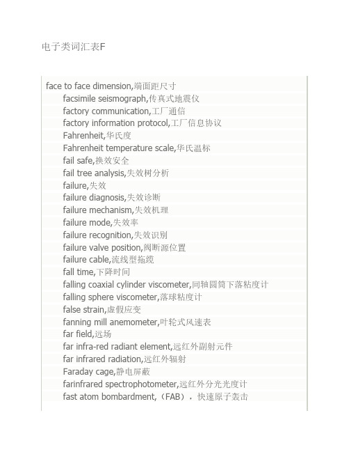
电子类词汇表Fface to face dimension,端面距尺寸 facsimile seismograph,传真式地震仪 factory communication,工厂通信 factory information protocol,工厂信息协议 Fahrenheit,华氏度 Fahrenheit temperature scale,华氏温标 fail safe,换效安全 fail tree analysis,失效树分析 failure,失效 failure diagnosis,失效诊断 failure mechanism,失效机理 failure mode,失效率 failure recognition,失效识别 failure valve position,阀断源位置 failure cable,流线型拖缆 fall time,下降时间 falling coaxial cylinder viscometer,同轴圆筒下落粘度计 falling sphere viscometer,落球粘度计 false strain,虚假应变 fanning mill anemometer,叶轮式风速表 far field,远场 far infra-red radiant element,远红外副射元件 far infrared radiation,远红外辐射 Faraday cage,静电屏蔽 farinfrared spectrophotometer,远红外分光光度计 fast atom bombardment,(FAB),快速原子轰击 faster-than-real-time simulation,超实时仿真 fatigue,疲劳 fatigue characteristic,疲劳特性 fatigue failure,疲劳破裂 fatibue life,疲劳寿命 fatigue limit,疲劳极限 fatigue strain gauge,疲劳应变计 fatigue testing machine,疲劳试验机 fault,故障 feasibility,可行性 feasibility study,可行性研究 feasible cooordination,可行协调 feasible region,可行域 feature detection,特征检测 feedback,反馈 feedback compensation,反馈补偿 feedback control,反馈控制 feedback controller,反馈控制器 feedback elements,反馈元件 feedback gain,反馈增益 feedback loop,反馈回路 feedback path,反馈通路 feedback signal,反馈信号 feedforward,前馈 feedforward compensation,前馈补偿 feedforward control,前馈控制下 feedforward path,前馈通路 feedover,馈越 ferrodynamic galvanometer,铁磁电动系振动子 ferrodynamic instrument,铁磁电动系仪表 ferrograph,铁磁示波器 FET gas transducer[sensor],场效应(管)湿度传感器 fiber communication,光纤通信 fiducial error,引用误差 fiducial value,引用值;基值 field,字段;现场 field balancing,现场平衡 field balancing equipment,现场平衡设备 field coil,励磁线圈 field controller,磁场控制器 field data,现场数据 field desorption(FD),场解吸 field emission electron image,场发射电子象 field emission gun,场发射电子枪 field emission microscope,场发射显微镜 field ion emission microscope,场离子发射显微镜 field ionization source;FI source,场电离源 field test,现场试验 field of view,视场 field rdliability test,现场可靠性试验 field stop,视场光栏 field sweeping,场扫描 field-frequency lock,场频锁 fieldbus,现场总线 fieldbus control system(FCS),现场总线控制系统 filament image,灯丝象 filar suspended galvanometer,悬丝式检流计 file,文件;文卷 file maintenance,文卷维护 fill factor,占空因子;填充率 filled system thermometer,压力式温度计 filled thermal system,充灌式感温系统 film recording thermograph,照相温度(表) film sample,薄膜样品 film varstor,膜式电压敏电阻器 filter,滤光计;过滤器;滤波器;滤光板;滤线板 filter device,滤光装置 filtered electron image,过滤电子象 filtered electron lens,过滤电子透镜 final controlling element,终端控制元件;执行器 final state,终态 final controlling element,终端控制元件;执行器 final state,终态 final temperature,终了温度终止温度 Fineman nephoscope,法因曼测云器 finte automaton,有限自动机 fire behaviour,着火性能 fire integrity,整体着火性 fire resistance,耐火性 fire stability,对火稳定性 firmware,固件fish finder,鱼探仪 fitting,管件 five-component borehole magnetometer,井中五分量磁测井仪 fixed core,定铁芯 fixed(measuring)instrument,固定式(测量)仪表 fixed points method of calibration,定点法标定 fixed resistance input type volt ratio box,定阻输入式分压箱 fixed resistance output type volt ratio box,定阻输出式分压箱 fixed set point control,定值控制 fixed set point control system,定值控制系统 rixed-based natural frequency,固定基础固有频率 flag,标记 flame emission spectrometry,火焰发射光谱法 flame ionization detector(FID),火焰离子化检测器 flame photometric detector(FPD),火焰光度检测器 flame proof enclsoure(Ex d),隔爆外壳(Ex d) flame temperature detector,火焰温度检测器 flange pressure tappings,法兰取压口 flanged ends,法兰连接端 flangeless ends,无法兰连接端 flangeless valve,无法兰阀 flashing,闪阀 flaw echo,缺陷反射波 flaw resolution,缺陷分辨力 flaw sensitivity,缺陷灵敏度 flexible disk,软磁盘 flexible manufacturing system,柔性制造系统 flexible rotor,柔性转子 flexural critical speed,挠曲临界转速 flexural principl mode,挠曲主振型 flicker,闪烁 float,浮子 float and cable level measuring device,浮标和缆索式液闰测量装置 float barograph,浮子气压计 float level measuring device,浮子液位测量装置 float level reguator,浮子型液位调节阀 float level transducer[sensor],浮子-干簧管液位传感器 float tide gauge,浮子式验潮仪 floating accelerometer,重力式测波仪 floating ball,浮置输入 floating output,浮置输出 floppy disk drive,软磁盘机 flow chart,流程图表 flow coefficient,流量系数 flow conditioner[straightener],流动调整器[整直器] flow control,流量控制 flow corrector,流量修正器 flow diagram,流程图 flow elbow,流量弯管 flow measurement calibration device,流量测量校准装置 flow measuring device,流量测量装置 flow nozzle,流量喷嘴 flow profile,流动剖面 flow rate of mobile phase,流动相流速 flow sihnal,流量信号 flow stabilizer,流量稳定器 flow switch,流量开关 flow to close,流关 flow to open,流开 flow transducer[sensor],流量传感器 flowmeter,流量计 flow-rate,流量 flow-rate range,流量范围 fluctuation,波动(度) fluid damping galvanometer,液体阻尼振动子 fluidic flowmeter,射流流量计 fluorescence,荧光修正 fluorescence detector,荧光检测器 fluorescence effect,荧光效应 fluorescent image,荧光象 flurescent magnetic partcle,荧光磁粉 fluorescent magnetic particle inspection machine,荧光磁粉探伤机 fluorescent penetrant festing method,荧光渗透探伤法 fluorine plastic,氟塑料 fluorine rubber(viton),氟橡胶 fluorometer,荧光计 flush mounted(pressure)gauge,,嵌装压力表 flutter,颤振 flux constant,磁通常数 flux meter,磁通表 flux of radiation,辐射通量 fluxgate compass,磁通门罗盘 fluxgate magnetometer,磁通门磁力仪;磁通门磁强计 fluxmeter,磁通表 fluxmeter calibrator,磁通表校验仪 focal distance,焦距 focal plane,焦平面 focal point,焦点 focus,焦点 focus size,焦点尺寸 focus-to-film distance,焦距 focusing,聚焦 focusing type probe,聚焦探头 fog-gauge,雾量器 foil strain gauge,箔式应变计 folding chart[paper],折叠式记录纸 follow-up control,随动控制 follow-up pointer,从动针 food analyzer,食品分析仪 force,力 force-balance acceleration transducer,力平衡式加速度传感器 force-balance accelerometer,力平衡式加速度计 force convection,强近对流 force standard machine,力标准机 force transducer[sensor],力传感器 forced vibration,强迫振动;受迫振动 foregraound,前台 foreground processing,前台处理 foreground program,前台程序 form factor,波形因数 Fortin barometer,福丁气压表 forward channel,正向信道 Foundation Fieldbus(FF),基金会现场总线;FF总线 four-terminal standard resistor,四端(钮)标准电阻器 Fourier transform,傅里叶变换 Fouier transform ion cyclotron resonance mass spertrometer (FT-ICR-MS), 傅立叶变换离子回旋共振质谱计 Fourier transform infrared spectrometry,傅立叶变换红外光谱法 Fourier transform spectrometer,傅里叶变换光谱仪 fracture toughness,断裂韧性 fragment ion,碎片离子 fragmentation,碎裂过程 frqgmentation pattern,碎裂图型 frame,帧 framework,框架 free falling STD profilinge system,自返式温盐深剖面仪 free field,自由声场 free field correction curves,自由场修正曲线 free-field frequency response of microphone,传声器自由声场频率响应 free feild reciprocity calibration,自由声场互易校准 free-field sensitivity of microphone,传声器自由声场灵敏度 free induction decay signal;FID signal,自由感应衰减信号 free oscillating period,自由振动周期 free swing of pendulum,摆锤空击 free vehicle respirometer,活动式海底生物呼吸测量器 free vibration,自由振动 freezing heat,凝固热 freezing point,凝固点 frequency,频率 frequency-amplitude characteristic,幅频特性 frequency analysis,频率分析 frequency analyzer,频率分析仪 frequency band,频带 frequency distrbution,频率分布 frequency division multiplexing,频分多路传输 frequency domain,频域 frequency domain analysis,频域分析 frequency domain method,频域法 frequency domain model reduction method,频域模型降价法 frequency index,频率指数 frequency measurement by comparison with time scale,时标比较法测频 frequency measurement by digital meter,用数字频率计测频 frequency measurement by Lissajou's figure,用李沙育图形测频 frequency measurement by stroboscope,闪光测频 frequency measurement by vibrationg reed indicator,用舌簧频率计测频 frequency meter,频率表 frequency modulation(FM),频率周制,调频 frequency of the natural hydraulic mode,液压固有频率 frequency output,频率输出 frequency-phase characteristic,相频特性 frequency response,频率响应 frequency response characteristics,频率响应特性(图) frequency reponse locus,频率响应轨迹图 frequency response of microphone,传声器频率响应 frequency response range,频率响应范围 frequency resonse tracer,频率响应显示仪 frequency shift keying(FSK),频移键控 frequency shift magnetometer,频移磁强计frequency sounding instrument,频率测深仪 frequency spectra induced polarization instrument,频谱激电仪 frequency stabilization,频率稳定 frequency sweeping,频率扫描 frequency-temperature coefficient,频率-温度系数 Fresnal diffraction string,费涅尔衍射条纹 friction bezel ring,压紧盖环 friction error,轻敲位移 friction velocity,磨擦速度 front end processor,前端处理机 frontal chromatography,迎头色谱法 frost point hygrometer,霜点湿度计(表) full bridge measurement,全桥测量 full capacity trim,全容量阀内件 full-load test,满载试验 full scale flow-rate,满标度流量 full-screen editing,全屏莫编辑 full-screen processing(FSP),全屏幕处理 full-wave logger,声波全波列测井仪 fully developed velocity distrbution,充分发展的速度分布 fully insulated current transormer,全绝缘电流互感器 fully rough trbulent flow,充分混杂紊流 function,功能 function analysis,功能分析 function block,功能块 function key,功能键 function module,功能模块 function type optic-fibre temperature transducer,功能型光纤温度传感器 functional block,功能块 functional decomposition,功能分解 functional insulation,功能绝缘 functional similarity,功能相似 functional simulation,功能仿真 fundamental frequency,基本频率 fundamental method of measurement,基础测量法 fundamental natural mode of vibration,基本固有振型 fundamental period,基本周期 fundamental wave,基波 funnel-shaped mud viscometer,漏斗式泥浆粘度计 furnace for reproduction of fixed points,定点炉 furnace for verification use,检定炉 fuzzy control,模糊控制 fuzzy controller,模糊控制器 fuzzy decision,模糊决策 fuzzy game,模糊对策 fuzzy information,模糊信息 fuzzy logic,模糊逻辑。

Digital Zero-Height SiSonic TM Microphone With Multiple Performance ModesThe SPH0641LM4H-1 is a miniature, high-performance, low power, bottom port silicon digital microphone with a single bit PDM output. Using Knowles’ proven high performance SiSonic TM MEMS technology, the SPH0641LM4H-1 consists of an acoustic sensor, a low noise input buffer, and a sigma-delta modulator. These devices are suitable for applications such as cellphones, smart phones, laptop computers, sensors, digital still cameras, portable music recorders, and other portable electronic devices where excellent wideband audio performance and RF immunity are required. In addition, the SPH0641LM4H-1 offers multiple performance modes Features:∙High SNR of 64dB∙Low Current Consumption of 230uA in Low-Power Mode∙Flat Frequency Response∙RF Shielded∙Zero-Height Mic TM∙Supports Dual Multiplexed Channels ∙Standard SMD Reflow∙Omnidirectional∙Multiple performance modes (Sleep, Low-Power, Standard Performance) ∙Sensitivity Matching∙Small Size1.ABSOLUTE MAXIMUM RATINGSStresses exceeding these “Absolute Maximum Ratings” may cause permanent damage to the device. These are stress ratings only. Functional operation at these or any other conditions beyond those indicated under “Acoustic& Electrical Specifications” is not implied. Exposure beyond tho se indicated under “Acoustic & Electrical Specifications” for extended periods may affect device reliability.2. ACOUSTIC & ELECTRICAL SPECIFICATIONSTEST CONDITIONS: 23 ±2°C, 55±20% R.H., V DD=1.8 V, f CLOCK=2.4 MHz, SELECT pin grounded, no load, unless otherwise indicatedStandard Performance Mode TEST CONDITIONS: f = 2.4 MHz, V=1.8 V, unless otherwise indicatedLow-Power ModeMicrophone Interface Specifications2 Ivaries with C LOAD according to: ΔI DD = 0.5*V DD*ΔC LOAD*f CLOCK.DD3 Typical and Maximum specifications are measured at standard test conditions.4 Valid microphones states are: Powered Down Mode (mic off), Sleep Mode (low current, DATA = high-Z, fast startup), Low-Power Mode (low clock speed) and Standard Performance Mode (normal operation).5 Time from f< 250 kHz to I SLEEP specification is met when transitioning from Active Mode to Sleep Mode.CLOCK6 Time from f≥ 351 kHz to all applicable specifications are met when transitioning from Sleep Mode to Active Mode.CLOCK7 tis dependent on C LOAD.HOLD3.MICROPHONE STATE DIAGRAM4.FREQUENCY RESPONSE CURVE5. INTERFACE CIRCUITNote: Bypass capacitors near each Mic V DD PIN are recommented to provide maximum SNRperformance. It should not contain Class 2 dielectrics. Detailed information on acoustic, mechanical, and system integration can be found in the latest SiSonic TM Design Guide application note.6. TIMING DIAGRAMV DD V DD SELECT Mic (High)DATA CLOCK Mic (Low)SELECTt EDGEDATA (SELECT = V t DDt DV t DZ CLOCKDATAV IHILt DVt DZHigh ZMic (Low) Data High ZMic (High) Data V OHV OLt EDGEV OHV OL1/F CLOCKt DDt HOLDt HOLD7.MECHANICAL SPECIFINotes: Pick Area only extends to 0.25 mm of any edge or hole unless otherwise specified.Dimensions are in millimeters unless otherwise specified.Tolerance is ±0.15mm unless otherwise specified8.EXAMPLE LAND PATTERN9.EXAMPLE SOLDER STENCIL PATTERNNotes: Dimensions are in millimeters unless otherwise specified.Detailed information on AP size considerations can be found in the latest SiSonic TM Design Guide application note.Further optimizations based on application should be performed.10. PACKAGING & MARKING DETAILAlpha Character A:“S ”: Knowles SiSonic TM Production “E ”: Knowles Engineering Samples “P”: Knowles Prototype Samples “JIN NUMBER”:Unique Job Identification Number for product traceabilityNotes: Dimensions are in millimeters unless otherwise specified.Vacuum pickup only in the pick area indicated in Mechanical Specifications. Tape & reel per EIA-481.Labels applied directly to reel and external package.Shelf life: Twelve (12) months when devices are to be stored in factory supplied, unopened ESD moisture sensitive bag under maximum environmental conditions of 30°C, 70% R.H.Pin 111. RECOMMENDED REFLOW PROFILENotes: Based on IPC/JDEC J-STD-020 Revision C.All temperatures refer to topside of the package, measured on the package body surface.T e m p e r a t u r eTime 25°C to PeakRamp-downRamp-upT SMINT SMAX T L T Pt Lt Pt S PreheatTime25°C12.ADDITIONAL NOTES(A)MSL (moisture sensitivity level) Class 1.(B)Maximum of 3 reflow cycles is recommended.(C)In order to minimize device damage:∙Do not board wash or clean after the reflow process.∙Do not brush board with or without solvents after the reflow process.∙Do not directly expose to ultrasonic processing, welding, or cleaning.∙Do not insert any object in port hole of device at any time.∙Do not apply over 30 psi of air pressure into the port hole.∙Do not pull a vacuum over port hole of the microphone.∙Do not apply a vacuum when repacking into sealed bags at a rate faster than 0.5 atm/sec.13.MATERIALS STATEMENTMeets the requirements of the European RoHS directive 2011/65/EC as amended.Meets the requirements of the industry standard IEC 61249-2-21:2003 for halogenated substances and Knowles Green Materials Standards Policy section on Halogen-Free.Ozone depleting substances are not used in the product or the processes used to make the product, including compounds listed in Annex A, B, and C of the “Montreal Protocol on Substances That Deplete the Ozone Layer.”14.RELIABILITY SPECIFICATIONSNote: After reliability tests are performed, the sensitivity of the microphones shall not deviate more than 3 dB from its initial value.After 3 reflow cycles, the sensitivity of the microphones shall not deviate more than 1 dB from its initial value.15.SPECIFICATION REVISIONSInformation contained herein is subject to change without notice. It may be used by a party at their own discretion and risk. We do not guarantee any results or assume any liability in connection with its use. This publication is not to be taken as a license to operate under any existing patents.Mouser ElectronicsAuthorized DistributorClick to View Pricing, Inventory, Delivery & Lifecycle Information:K nowles:SPH0641LM4H-1SPH1668LM4-1。

SPECIFICA TIONSPXI-592224-Bit, Flexible Resolution PXI OscilloscopeContents Definitions (2)Conditions (2)Vertical (2)Analog Input (2)Impedance and Coupling (3)V oltage Levels (3)Accuracy (3)Bandwidth and Transient Response (4)Spectral Characteristics (6)Skew, Input Bias Current (9)Settling Time (10)Horizontal (11)Sample Clock (11)Onboard Clock (Internal VCXO) (11)Phase-Locked Loop (PLL) Reference Clock (12)Trigger (13)Reference (Stop) Trigger (13)External Trigger (14)PFI 0 and PFI 1 (Programmable Function Interface, AUX Front Panel Connectors) (14)Waveform Specifications (15)Calibration (16)Software (16)Driver Software (16)Application Software (16)Interactive Soft Front Panel and Configuration (16)TClk Specifications (17)Power (17)Physical (18)Environment (18)Operating Environment (18)Storage Environment (18)Shock and Vibration (19)Compliance and Certifications (19)Safety (19)Electromagnetic Compatibility (19)CE Compliance (20)Online Product Certification (20)Environmental Management (20)DefinitionsWarranted specifications describe the performance of a model under stated operating conditions and are covered by the model warranty. Warranted specifications account for measurement uncertainties, temperature drift, and aging. Warranted specifications are ensured by design, or verified during production and calibration.The following characteristic specifications describe values that are relevant to the use of the model under stated operating conditions but are not covered by the model warranty.•Typical specifications describe the performance met by a majority of models.•Nominal specifications describe an attribute that is based on design, conformance testing, or supplemental testing.•Measured (meas) specifications describe the measured performance of a representative model.Specifications are Typical unless otherwise noted.ConditionsSpecifications are valid under the following conditions unless otherwise noted.•Full operating temperature range•All impedance selections•All sample rates•Source impedance ≤50 ΩSpecifications are valid under the following conditions unless otherwise noted:•Ambient temperatures of 15 °C to 35 °CVerticalAnalog InputNumber of channels Software-selectable: two simultaneouslysampling, single-ended or unbalanceddifferential channels or one differential channel Connector BNC2| | PXI-5922 SpecificationsImpedance and CouplingInput impedance Software-selectable: 50 Ω ±2.0% or 1 MΩ±2.0% in parallel with a nominal capacitanceof 60 pFInput coupling AC, DC, GNDVoltage LevelsFull-scale (FS) input range±1 V (2 V pk-pk)±5 V (10 V pk-pk)Maximum input overload50 Ω7 V rms with |Peaks| ≤10 V1 MΩ|Peaks| ≤42 VAccuracyDC accuracy, Warranted12 V pk-pk range±(0.05%) of input + 50 μV)10 V pk-pk range±(0.05%) of input + 100 μV)DC drift, nominal22 V pk-pk range±(.002% of input + 5 μV per °C)10 V pk-pk range±(.002% of input + 10 μV per °C)1 1 MΩ input impedance; within ±5 °C of self-calibration temperature; ppm = parts per million (1 ×10 -6 ).2 1 MΩ input impedance.PXI-5922 Specifications| © National Instruments| 3AC amplitude accuracy 0.06% at 1 kHz 3Crosstalk 4At 100 kHz ≤-110 dB At 1 MHz ≤-100 dB At 6 MHz≤-80 dBCommon-mode rejection ratio (CMRR)50 dB up to 1 kHz 5Figure 1. PXI-5922 CMRR with Differential T erminal Configuration, Measured100 k1 M 10 M10 k 1001 k –40–50–60–70–80–90–100C M R R (d B)Frequency (Hz)Bandwidth and Transient ResponseAlias-free bandwidth0.4 × Sample Rate63 1 MΩ input impedance; within ±5 °C of self-calibration temperature.4CH 0 to/from CH 1, External Trigger to CH 0 or CH 1.5Unbalanced differential input terminal configuration.6Input frequencies ≥ 0.6 × Sample Rate .4 | | PXI-5922 SpecificationsTable 2. Alias Protection 6 (Continued)AC coupling cutoff (-3 dB)90 Hz7Figure 2. 100 kS/s Frequency Response, MeasuredFrequency (Hz)20 k 30 k 10 k40 k0.2–0.2–0.100.1P h a s e (d e g r e e s )Frequency (Hz)10 k20 k 30 k 40 k50 k0.2–0.2–0.100.1A m p l i t u d e (d B )6Input frequencies ≥ 0.6 × Sample Rate .7Referenced to DC; input frequencies up to 0.4 × Sample Rate .PXI-5922 Specifications | © National Instruments | 5Figure 3. 1 MS/s Frequency Response, MeasuredFrequency (Hz)0200 k 300 k 100 k400 k0.2–0.2–0.100.1P h a s e (d e g r e e s )Frequency (Hz)100 k200 k 300 k 400 k500 k0.2–0.2–0.100.1A m p l i t u d e (d B )Figure 4. 10 MS/s Frequency Response, MeasuredFrequency (Hz)2 M3 M 1 M4 M1–1–0.500.5P h a s e (d e g r e e s )Frequency (Hz)1 M2 M3 M4 M5 M0.2–0.2–0.100.1A m p l i t u d e (d B )Spectral Characteristics88-1 dBFS input signal; Sample Rate is 10 × input frequency; within ±2 °C of self-calibration temperature.6 | | PXI-5922 SpecificationsFigure 5. PXI-5922 Dynamic Performance with 10 kHz Input Signal, Measured,1 M Ω,10 V pk-pk Range, 500 kS/s, Unbalanced Differential, 10,000-Point FFT with 10 Averages–200–40–60–80–100–120–140–160255075100125150175200225250A m p l i t u d e (dB F S )Frequency (kHz)Figure 6. PXI-5922 Dynamic Performance with 10 kHz Input Signal, Measured, 1 M Ω,2 V pk-pk Range, 100 kS/s, Unbalanced Differential, 10,000-Point FFT with 10 Averages50454035302520151050–20–40–60–80–100–120–140–160A m p l i t u d e (dB F S )Frequency (kHz)PXI-5922 Specifications | © National Instruments | 7Table 5. Total Harmonic Distortion (THD)910Table 7. Signal-to-Noise Ratio (SNR) without Harmonics119-1 dBFS input signal; includes the second through the fifth harmonics; within ±2 °C of self-calibration temperature .10-1 dBFS input signal; input frequency is 0.1 × Sample rate; within ±2 °C of self-calibration temperature; calculated from THD and RMS noise.11-1 dBFS input signal; input frequency is 0.1 × Sample rate; within ±2 °C of self-calibration temperature; calculated from SINAD and THD.8| | PXI-5922 SpecificationsTable 8. RMS Noise, Warranted 12Figure 7.PXI-5922 Noise Density, MeasuredN o i s e D e n s i t y (d B F S /H z )Frequency (Hz)Skew, Input Bias CurrentChannel-to-channel skew 13≤500 psInput bias current 14≤500 nA, Warranted12100 Hz to 0.4 × Sample rate ; DC coupling; input 50 Ω terminated.13 1 MHz input, 5 MS/s sample rate.14Within ±5 °C of self-calibration temperature.PXI-5922 Specifications | © National Instruments | 9Settling Time15Figure 8.PXI-5922 Step Response Using Different Filter T ypes, Measured 172.0 µ1.8 µ1.6 µ1.4 µ1.2 µ1.0 µ800 n 600 n 400 n 200 n 03.53.02.52.01.51.00.50.0–0.5Time (seconds)A m p l i t u d e (V )15For a 3 V step from 0 V DC, excluding noise; time referenced to 1.5 V (50%) trigger; applies to 15 MS/s sample rate only.16To set or change the filter type, use the Flex FIR Antialias Filter Type property or the NISCOPE_ATTR_FLEX_FIR_ANTIALIAS_FILTER_TYPE attribute.17Time (t= 0) represents the actual time the edge arrived at the BNC connector on the NI 5922.10 | | PXI-5922 SpecificationsFigure 9. PXI-5922 Frequency Response Using Different Filter Types, Measured100–90–80–70–60–50–40–30–20–10–100A m p l i t u d e (dB )Frequency (Hz)HorizontalSample ClockSourcesInternal onboard clock (internal VCXO)18Onboard Clock (Internal VCXO)Sample rate range, real-time sampling (single shot)1950 kS/s to 15 MS/sPhase noise density (5 MHz input signal)At 10 kHz <-133 dBc/Hz At 100 kHz <-145 dBc/HzSample clock jitter 20≤3 ps rms (100 Hz to 1 MHz)Timebase frequency120 MHz 18Internal Sample clock is locked to the Reference clock or derived from the onboard VCXO.19Available rates are (60 MS/s) /n where n is an integer value from 4 to 1200. The Sample clock period is n/(60MS/s).20Includes the effects of the converter aperture uncertainty and the clock circuitry jitter; excludes trigger jitter.Timebase accuracyNot phase-locked to Reference clock±50 ppm, WarrantedPhase-locked to Reference clock Equal to the Reference clock accuracy Sample clock delay range±1 Sample clock periodSample clock delay resolution400 psPhase-Locked Loop (PLL) Reference ClockReference clock sources PXI_CLK 10 (backplane connector)CLK IN (front panel SMB connector) Frequency range 1 MHz to 20 MHz in 1 MHz increments21;must be accurate to ±50 ppmDuty cycle tolerance45% to 55%Exported Reference clock destinations CLK OUT (front panel SMB connector)PFI <0..1> (front panel 9-pin mini-circularDIN connector)PXI_TRIG <0..6> (backplane connector) CLK IN (Reference Clock Input, Front Panel Connector)Input voltage range Square wave: 0.2 V pk-pk to 1 V pk-pk Maximum input overload7 V rms with |Peaks| ≤ 10 VImpedance50 ΩCoupling ACCLK OUT (Reference Clock Output, Front Panel Connector) Output impedance50 ΩLogic type 5 V CMOSMaximum drive current±50 mA21The default value is 10 MHz.T riggerReference (Stop) TriggerTrigger types EdgeWindowHysteresisDigitalImmediateSoftwareTrigger sources CH 0CH 1TRIGPXI_Trig <0..6>PFI <0..1>PXI Star TriggerRTSI <0..6>SoftwareTime resolution Sample clock periodRearm time144 × Sample clock period22Holdoff Up to (232 - 1) × Sample clock period Related InformationRefer to the NI High-Speed Digitizers Help for more information about the sources available for each trigger type.Analog TriggerTrigger types EdgeWindowHysteresisSources23CH 0 (front panel BNC connector)CH 1 (front panel BNC connector)TRIG (front panel BNC connector)Trigger level range100% FS22Holdoff set to 0.23TRIG is an analog edge trigger only.Edge trigger sensitivityCH 0, CH 12% FSTRIG (external trigger)0.3 V pk-pk up to 1 MHzJitter Sample clock periodDigital TriggerTrigger type DigitalSources PXI_TRIG <0..6> (backplane connector)PFI <0..1> (front panel 9-pin DIN connectorPXI Star Trigger (backplane connector) External T riggerSource TRIG (front panel BNC connector) Impedance100 kΩ in parallel with 52 pF, nominal Input voltage range±2.5 VCoupling DCLevel accuracy±0.3 V up to 100 kHzMaximum input overload|Peaks| ≤42 VPFI 0 and PFI 1 (Programmable Function Interface, AUX Front Panel Connectors)Connector9-pin mini-circular DINDirection BidirectionalAs an Input (T rigger)Destinations Start trigger (acquisition arm)Reference (stop) triggerArm Reference triggerAdvance triggerInput impedance150 kΩ , nominalV IH 2.0 VV IL0.8 VMaximum input overload-0.5 V, 5.5 VMaximum frequency25 MHzAs an Output (Event)Sources Start trigger (acquisition arm)Reference (stop) triggerEnd of RecordDone (end of acquisition)Output impedance50 ΩLogic type 3.3 V CMOSMaximum drive current±24 mAMaximum frequency20 MHzWaveform SpecificationsOnboard memory size8 MB/channel 2 MS/channel32 MB/channel8 MS/channel256 MB/channel64 MS/channelMinimum record length 1 SampleNumber of pretrigger samples0 up to full Record Length for both single-record mode and multiple-record mode Number of posttrigger samples0 up to full Record Length for both single-record mode and multiple-record mode Maximum number of records in onboard memory248 MB/channel13,10732 MB/channel52,428256 MB/channel100,000Allocated onboard memory per record(Record Length × 4 bytes/S) + 400 bytes,rounded up to next multiple of 128 bytes or640 bytes, whichever is greater 24It is possible to exceed these numbers if you fetch records while acquiring data. For more information, refer to the NI High-Speed Digitizers Help.CalibrationSelf-calibration Self-calibration is done on software command.The calibration corrects for gain and offset forall input ranges, input bias current, andnonlinearities in the ADCs.External calibration (factory calibration)The external calibration calibrates the VCXOand the voltage reference. Appropriateconstants are stored in nonvolatile memory. Interval for external calibration 2 yearsWarm-up time15 minutesSoftwareDriver SoftwareDriver support for this device was first available in NI-SCOPE 2.8.NI-SCOPE is an IVI-compliant driver that allows you to configure, control, and calibrate the PXI-5922. NI-SCOPE provides application programming interfaces for many development environments.Application SoftwareNI-SCOPE provides programming interfaces, documentation, and examples for the following application development environments:•LabVIEW•LabWindows™/CVI™•Measurement Studio•Microsoft Visual C/C++•.NET (C# and )Interactive Soft Front Panel and ConfigurationWhen you install NI-SCOPE on a 64-bit system, you can monitor, control, and record measurements from the PXI-5922 using InstrumentStudio.InstrumentStudio is a software-based front panel application that allows you to perform interactive measurements on several different device types in a single program.Note InstrumentStudio is supported only on 64-bit systems. If you are using a 32-bit system, use the NI-SCOPE–specific soft front panel instead of InstrumentStudio. Interactive control of the PXI-5922 was first available via InstrumentStudio inNI-SCOPE 18.0 and via the NI-SCOPE SFP in NI-SCOPE 2.2. InstrumentStudio and the NI-SCOPE SFP are included on the NI-SCOPE media.NI Measurement & Automation Explorer (MAX) also provides interactive configuration and test tools for the PXI-5922. MAX is included on the driver media.TClk SpecificationsYou can use the NI TClk synchronization method and the NI-TClk driver to align the Sample clocks on any number of supported devices, in one or more chassis. For more information about TClk synchronization, refer to the NI-TClk Synchronization Help, which is located within the NI High-Speed Digitizers Help. For other configurations, including multichassis systems, contact NI Technical Support at /support.Intermodule SMC Synchronization Using NI-TClk for Identical ModulesSpecifications are valid under the following conditions:•Any number of PXI modules installed in one NI PXI-1042 chassis.•All parameters set to identical values for each SMC-based module.•Sample clock set to 15 MS/s and all filters disabled.Skew25500 psAverage skew after manual adjustment<10 psSample clock delay/adjustment resolution≤5 psRelated InformationFor information about manual adjustment, refer to the Synchronization Repeatability Optimization topic in the NI-TClk Synchronization Help within the NI High-Speed Digitizers Help.For additional help with the adjustment process, contact NI Technical support at / support.PowerCurrent draw+3.3 VDC 2.0 A+5 VDC 1.4 A+12 VDC330 mA-12 VDC280 mATotal power20.9 W25Caused by clock and analog path delay differences. No manual adjustment performed.PhysicalDimensions3U, one-slot, PXI/cPCI module21.6 cm × 2.0 cm × 13.0 cm(8.5 in × 0.8 in × 5.1 in)Weight336 g (11.8 oz)EnvironmentMaximum altitude2,000 m (at 25 °C ambient temperature) Pollution Degree2Indoor use only.Note To ensure that the PXI-5922 cools effectively, follow the guidelines in theMaintain Forced-Air Cooling Note to Users included in the kit or available at/manuals. The PXI-5922 is intended for indoor use only. Operating EnvironmentAmbient temperature range0 °C to 55 °C in all NI PXI chassis except thefollowing: 0 °C to +45 °C when installed in anNI PXI-1000/B or PXI-101x chassis. (Tested inaccordance with IEC 60068-2-1 andIEC 60068-2-2.)Relative humidity range10% to 90%, noncondensing (Tested inaccordance with IEC 60068-2-56.) Storage EnvironmentAmbient temperature range-40 °C to 71 °C (Tested in accordancewith IEC 60068-2-1 and IEC 60068-2-2.) Relative humidity range5% to 95%, noncondensing (Tested inaccordance with IEC 60068-2-56.)Shock and VibrationOperational shock30 g peak, half-sine, 11 ms pulse (Tested inaccordance with IEC 60068-2-27. Test profiledeveloped in accordance withMIL-PRF-28800F.)Storage Shock50 g, half-sine, 11 ms pulse (Tested inaccordance with IEC 60068-2-27.Test profiledeveloped in accordance withMIL-PRF-28800F.)Random vibrationOperating 5 Hz to 500 Hz, 0.31 g rms (Tested inaccordance with IEC 60068-2-64.) Nonoperating 5 Hz to 500 Hz, 2.46 g rms (Tested inaccordance with IEC 60068-2-64. Test profileexceeds the requirements of MIL-PRF-28800F,Class 3.)Compliance and CertificationsSafetyThis product is designed to meet the requirements of the following electrical equipment safety standards for measurement, control, and laboratory use:•IEC 61010-1, EN 61010-1•UL 61010-1, CSA C22.2 No. 61010-1Note For UL and other safety certifications, refer to the product label or the OnlineProduct Certification section.Electromagnetic CompatibilityThis product meets the requirements of the following EMC standards for electrical equipment for measurement, control, and laboratory use:•EN 61326-1 (IEC 61326-1): Class A emissions; Basic immunity•EN 55011 (CISPR 11): Group 1, Class A emissions•EN 55022 (CISPR 22): Class A emissions•EN 55024 (CISPR 24): Immunity•AS/NZS CISPR 11: Group 1, Class A emissions•AS/NZS CISPR 22: Class A emissions•FCC 47 CFR Part 15B: Class A emissions•ICES-001: Class A emissionsNote In the United States (per FCC 47 CFR), Class A equipment is intended foruse in commercial, light-industrial, and heavy-industrial locations. In Europe,Canada, Australia, and New Zealand (per CISPR 11), Class A equipment is intendedfor use only in heavy-industrial locations.Note Group 1 equipment (per CISPR 11) is any industrial, scientific, or medicalequipment that does not intentionally generate radio frequency energy for thetreatment of material or inspection/analysis purposes.Note For EMC declarations, certifications, and additional information, refer to theOnline Product Certification section.CE ComplianceThis product meets the essential requirements of applicable European Directives, as follows:•2014/35/EU; Low-V oltage Directive (safety)•2014/30/EU; Electromagnetic Compatibility Directive (EMC)Online Product CertificationRefer to the product Declaration of Conformity (DoC) for additional regulatory compliance information. To obtain product certifications and the DoC for this product, visit / certification, search by model number or product line, and click the appropriate link in the Certification column.Environmental ManagementNI is committed to designing and manufacturing products in an environmentally responsible manner. NI recognizes that eliminating certain hazardous substances from our products is beneficial to the environment and to NI customers.For additional environmental information, refer to the Minimize Our Environmental Impact web page at /environment. This page contains the environmental regulations and directives with which NI complies, as well as other environmental information not included in this document.Waste Electrical and Electronic Equipment (WEEE)EU Customers At the end of the product life cycle, all NI products must bedisposed of according to local laws and regulations. For more information abouthow to recycle NI products in your region, visit /environment/weee.电子信息产品污染控制管理办法(中国RoHS)中国客户National Instruments符合中国电子信息产品中限制使用某些有害物质指令(RoHS)。

Simply VersatileSP60 GNSS ReceiverSP60GNSS ReceiverThe Spectra Precision SP60 is a newgeneration GNSS receiver offering ahigh level of flexibility to cover anydemand from GIS all the way up tosophisticated RTK and Trimble RTX™capable solutions.Combining the unique all-signals-tracking and processing Z-BladeGNSS-centric technology and L-bandcapability for satellite-delivered TrimbleRTX correction services, the SP60receiver provides the most reliablemeasurements and the highest possibleaccuracy under any conditions anywherein the world.Key features■■Extended scalability■■Z-Blade GNSS-centric technology■■240-channel 6G ASIC■■Anti-theft technology■■Long Range Bluetooth■■Trimble RTX correction servicesPatentedinside-the-rodmounted UHFantenna design SP6Truly scalable and versatileExtremely scalable and versatile, SP60 can respond to any type of GIS or surveying job starting with two GIS configurations, to a simple L1 GPS only post-processing solution, all the way up to dual-frequency GNSS network RTK rover. Also, the L-band capable GNSS antenna delivers Trimble RTX positioning in those places where an RTK network is not available. Finally, optional UHF transmit radio or embedded Long Range Bluetooth enable SP60 receivers to be used as a base and rover system. This extended flexibility allows surveyors to start with a simple solution, and through hardware and firmware upgrades, adapt the SP60 to more complex survey jobs.Unique 6G GNSS-centric technologyExclusive Z-Blade processing technology running on a next-generation Spectra Precision 240-channel 6G ASIC fully utilizes all 6 GNSS systems: GPS, GLONASS, BeiDou, Galileo, QZSS and SBAS. The unique GNSS-centric capability optimally combines GNSS signalswithout dependency on any specific GNSS system; this allows SP60 to operate in GPS-only, GLONASS-only or BeiDou-only mode if needed. Thanks to this unique GNSS technology, SP60 is optimized for tracking and processing signals even in very challenging environments.Trimble RTX capableTrimble RTX correction services offer a wide range of accuracy requirements ranging from better than 4 cm accuracies, up to sub-meter accuracies, without the need of an RTK base station or cellular coverage. Trimble RTX is available via both satellite and cellular/IP delivery. The premium service, CenterPoint ® RTX is the most accurate satellite-delivered correction service available today. The SP60,empowered with an L-band GNSS antenna, supports the entire suite of Trimble RTX correction services via satellite delivery and is ideal for operating in areas where there is no network available and a local base and rover set-up is not possible. With the SP60 GNSS receiver and a Trimble RTX correction, achieve high-accuracy positioning nearly anywhere in the world.Open to 3rd party controllers and applicationsWith SP60, consumer devices are no longer limited by their internal GPS and can reach mapping grade or even survey-grade accuracy levels. This solution is also open to any application needing to get an accurate position. The SPace application makes integration immediate and straightforward. With SP60 it is now possible to have accurate positions on an Android consumer smart phone or tablet.Built-in Long Range BluetoothSP60 integrates powerful Long Range Bluetooth capabilities opening new operating modes for surveyors. Now, the Bluetooth wirelesscommunication can be used as an alternative radio link between base and rover over a few hundred meters range making this solution very attractive for small site surveys. Easier and simpler than UHF radio, and without any need for a license, this can be a very efficient way to quickly setup a short range base rover solution.Anti-theft technologyUnique anti-theft technology secures SP60 when installed as a field base station in remote or public places and can detect if the product is disturbed, moved or stolen. This technology allows the surveyor to lock the device to a specific location and make it unusable if the device is moved elsewhere. In this case, SP60 will generate an audio alert and block the device from further use. SP60’s anti-theft technology provides surveyors with remote security and peace of mind.Advanced designIn addition to the cutting-edge L-band capable GNSS antenna, and unique Long Range Bluetooth module, the SP60 GNSS receiverdesign incorporates a number of innovative ideas and enhancements. It features a rugged, impact-resistant housing, easily withstanding 2m pole drops. Waterproof to IP67 standard, it can handle thetoughest outdoor conditions. The patented UHF antenna, set inside the fiberglass rod, extends the range of RTK radio performance and provides protection at the same time. All of these enhancements make the design of SP60 GNSS receiver truly unique and powerful.The Spectra Precision experienceSpectra Precision Survey Pro or FAST Survey field software provides easy-to-use, yet powerful GNSS workflows, letting the surveyor concentrate on getting the job done. Spectra Precision Survey Office Software provides a complete office suite for data processing and Spectra Precision Central cloud computing solution offers a simple to use pathway to data exchange and management. When combined with the most advanced and rugged field data collectors from Spectra Precision, SP60is a very powerful and complete solution.GNSS characteristics■■240 GNSS channels- GPS L1C/A, L1P(Y), L2P(Y), L2C - GLONASS L1C/A, L2C/A, L3- BeiDou B1 (phase 2), B2- Galileo E1, E5b- QZSS L1C/A, L2C, L1SAIF - SBAS L1C/A - L-band■■Support for Trimble RTX TM real-time correction services■■Patented Z-Blade technology for optimal GNSS performance- Full utilization of signals from all 6 GNSS systems (GPS, GLONASS, BeiDou, Galileo, QZSS and SBAS)- Enhanced GNSS-centric algorithm: fully-independent GNSS signal tracking and optimal data processing, including GPS-only, GLONASS-only or BeiDou-only solution (autonomous to full RTK)- Fast Search engine for quick acquisition and re-acquisition of GNSS signals■■Patented SBAS ranging for using SBAS code & carrier observations and orbits in RTK processing■■Patented Strobe ™ Correlator for reduced GNSS multi-path■■Up to 10 Hz real-time raw data (code & carrier and position output)■■Supported data formats: ATOM, CMR, CMR+, RTCM 2.1, 2.3, 3.0, 3.1 and 3.2 (including MSM), CMRx and sCMRx (rover only)■■NMEA 0183 messages outputReal-Time accuracy (RMS) (1)(2)SBAS (WAAS/EGNOS/MSAS/GAGAN) ■■Horizontal: < 50 cm ■■Vertical: < 85 cm Real-Time DGPS position■■Horizontal: 25 cm + 1 ppm ■■Vertical: 50 cm + 1 ppmReal-Time Kinematic position (RTK) ■■Horizontal: 8 mm + 1 ppm ■■Vertical: 15 mm + 1 ppm GIS accuracy modes ■■30/30- Horizontal: 30 cm - Vertical: 30 cm■■7/2 (firmware option needed)- Horizontal: 7 cm - Vertical: 2 cmReal-Time performance■■Instant-RTK ®Initialization- Typically 2 sec for baselines < 20 km - Up to 99.9% reliability■■RTK initialization range: over 40 kmPost-Processing accuracy (RMS) (1)(2)Static & Fast static■■Horizontal: 3 mm + 0.5 ppm ■■Vertical: 5 mm + 0.5 ppm High-Precision Static (3)■■Horizontal: 3 mm + 0.1 ppm ■■Vertical: 3.5 mm + 0.4 ppm Post-Processed Kinematic (PPK)■■Horizontal: 8 mm + 1 ppm ■■Vertical: 15 mm + 1 ppmData logging characteristicsRecording interval ■■0.1 - 999 secondsPhysical characteristicsSize■■21 x 21 x 7 cm (8.3 x 8.3 x 2.3 in)Weight■■930 g (2.08 lb)User interface■■Five LEDs for Power, Tracking, Bluetooth, Recording, Radio operations I/O interface■■RS232 serial link■■USB 2.0/UART and USB OTG■■Bluetooth 2.1 + EDR. Long range: Class 1 (19dbm)Memory■■256 MB internal memory NAND Flash■■Over a month of 15 sec. raw GNSS data from 14 satellites Operation■■RTK rover & base■■RTK network rover: VRS, FKP , MAC ■■NTRIP , Direct IP ■■Post-processing■■Trimble RTX (satellite and cellular/IP)Environmental characteristics■■Operating temperature: -40° to +65°C / (-40° to +149°F) (4)■■Storage temperature: -40° to +85°C / (-40° to +185°F) (5)■■Humidity: 100% condensing■■IP67 waterproof, sealed against sand and dust■■Drop: 2m pole drop on concrete ■■Shocks: MIL STD 810 (fig 516.5-10) (01/2000)■■Vibration : MIL-STD-810F (fig 514.5C-17) (01/2000)Power characteristics■■Li-Ion battery, 7.4 V, 2600 mAh ■■Battery life:10 hrs (GNSS On, UHF Rx Off) 8 hrs (GNSS On, UHF Rx On)■■External DC power: 9-28 V Standard system components ■■SP60 receiver ■■Li-Ion battery■■Dual battery charger, power supply and international power cord kit ■■Tape measure (3.6 m / 12 ft)■■7 cm pole extension ■■USB to mini-USB cable ■■ 2 year warrantyOptional system components■■SP60 UHF Kit (410-470 MHz 2W TRx)■■SP60 Field Power Kit ■■SP60 Office Power Kit ■■Data collectors - Ranger 3- T41- MobileMapper 50- ProMark 120- Nomad 1050■■Field software- Survey Mobile (Android)- SPace control app for 3rd party devices (Android)- Survey Pro - FAST Survey - ProMark Field(1) A ccuracy and TTFF specifications may be affected byatmospheric conditions, signal multipath, satellite geometry and corrections availability and quality.(2) P erformance values assume minimum of five satellites, followingthe procedures recommended in the product manual. High multipath areas, high PDOP values and periods of severe atmospheric conditions may degrade performance.(3) L ong baselines, long occupations, precise ephemeris used (4) A t very high temperatures UHF module should not be used in thetransmitter mode. With UHF transmitter on radiating 2W of RF power, the operating temperature is limited to + 55°C (+131°F).(5) W ithout batteries. Batteries can be stored up to +70°C.(6) R eceiver initialization time varies based on GNSS constellationhealth, level of multipath, and proximity to obstructions such as large trees and buildings.SP60 Technical SpecificationsPlease visit for the latest product information and to locate your nearest distributor.© 2016, Trimble Inc. All rights reserved. Spectra Precision and the Spectra Precision logo are trademarks of Trimble Inc or its subsidiaries. All other trademarks are the property oftheir respective owners. Windows and the Windows logo are trademarks or registered trademarks of Microsoft Corporation in the United States and/or other countries. (2016/10)Trimble RTX Initialization (1)(2)(6)Contact Information:AMERICAS10368 Westmoor DriveWestminster, CO 80021, USA +1-720-587-4700 Phone888-477-7516 (Toll Free in USA)EUROPE, MIDDLE EAST AND AFRICA Rue Thomas EdisonZAC de la Fleuriaye - CS 6043344474 Carquefou (Nantes), France +33 (0)2 28 09 38 00 PhoneASIA-PACIFIC80 Marine Parade Road #22-06, Parkway Parade Singapore 449269, Singapore +65-6348-2212 Phone。

傅里叶红外光谱的英文傅里叶红外光谱的英文I. IntroductionInfrared spectroscopy is a common analytical method used for studying the chemical properties of a sample. Fourier transform infrared spectroscopy (FTIR), also known as Fourier transform infrared (FTIR) analysis, is a type of infrared spectroscopy that uses a Fourier transform to obtain the spectral information. In this article, we will discuss the English terminology used for FTIR.II. Basic Terminology1. Infrared spectrum: a representation of the absorption or transmission of infrared radiation as a function of wavelength or frequency2. Spectral range: the range of wavelengths or frequencies measured in the infrared spectrum3. Wavenumber: the reciprocal of wavelength, measured in cm-1 in the FTIR spectrum4. Absorbance: the logarithm of the ratio of the incident radiation to the transmitted radiation, measured in the FTIR spectrum5. Peak: a point on the FTIR spectrum that corresponds to a specific vibrational mode of the sample6. Baseline: the absorption background in the FTIR spectrumIII. Sample PreparationBefore performing FTIR analysis, the sample must be prepared in the formof a thin film or powder to ensure uniformity of the sample.IV. InstrumentationFTIR analysis requires a Fourier transform infrared spectrometer, which consists of a source, interferometer, and detector. The sample is placed in the path of the infrared beam generated by the source and the transmitted or absorbed radiation is measured by the detector. The interferometer is used to obtain the interferogram, which is then transformed into the FTIR spectrum.V. ApplicationsFTIR is used in various fields such as chemistry, pharmaceuticals, and material science. It is commonly used for the identification of unknown compounds, characterization of functional groups, and monitoring of chemical reactions.VI. ConclusionFTIR analysis is a powerful technique for studying the chemical properties of a sample. Understanding the basic terminology and instrumentation used in FTIR is essential for accurate interpretation of the spectral data.。

AgilentDigital Modulation in Communications Systems—An IntroductionApplication Note 1298This application note introduces the concepts of digital modulation used in many communications systems today. Emphasis is placed on explaining the tradeoffs that are made to optimize efficiencies in system design.Most communications systems fall into one of three categories: bandwidth efficient, power efficient, or cost efficient. Bandwidth efficiency describes the ability of a modulation scheme to accommodate data within a limited bandwidth. Power efficiency describes the ability of the system to reliably send information at the lowest practical power level.In most systems, there is a high priority on band-width efficiency. The parameter to be optimized depends on the demands of the particular system, as can be seen in the following two examples.For designers of digital terrestrial microwave radios, their highest priority is good bandwidth efficiency with low bit-error-rate. They have plenty of power available and are not concerned with power efficiency. They are not especially con-cerned with receiver cost or complexity because they do not have to build large numbers of them. On the other hand, designers of hand-held cellular phones put a high priority on power efficiency because these phones need to run on a battery. Cost is also a high priority because cellular phones must be low-cost to encourage more users. Accord-ingly, these systems sacrifice some bandwidth efficiency to get power and cost efficiency. Every time one of these efficiency parameters (bandwidth, power, or cost) is increased, another one decreases, becomes more complex, or does not perform well in a poor environment. Cost is a dom-inant system priority. Low-cost radios will always be in demand. In the past, it was possible to make a radio low-cost by sacrificing power and band-width efficiency. This is no longer possible. The radio spectrum is very valuable and operators who do not use the spectrum efficiently could lose their existing licenses or lose out in the competition for new ones. These are the tradeoffs that must be considered in digital RF communications design. This application note covers•the reasons for the move to digital modulation;•how information is modulated onto in-phase (I) and quadrature (Q) signals;•different types of digital modulation;•filtering techniques to conserve bandwidth; •ways of looking at digitally modulated signals;•multiplexing techniques used to share the transmission channel;•how a digital transmitter and receiver work;•measurements on digital RF communications systems;•an overview table with key specifications for the major digital communications systems; and •a glossary of terms used in digital RF communi-cations.These concepts form the building blocks of any communications system. If you understand the building blocks, then you will be able to under-stand how any communications system, present or future, works.Introduction25 5 677 7 8 8 9 10 10 1112 12 12 13 14 14 15 15 16 17 18 19 20 21 22 22 23 23 24 25 26 27 28 29 29 30 311. Why Digital Modulation?1.1 Trading off simplicity and bandwidth1.2 Industry trends2. Using I/Q Modulation (Amplitude and Phase Control) to Convey Information2.1 Transmitting information2.2 Signal characteristics that can be modified2.3 Polar display—magnitude and phase representedtogether2.4 Signal changes or modifications in polar form2.5 I/Q formats2.6 I and Q in a radio transmitter2.7 I and Q in a radio receiver2.8 Why use I and Q?3. Digital Modulation Types and Relative Efficiencies3.1 Applications3.1.1 Bit rate and symbol rate3.1.2 Spectrum (bandwidth) requirements3.1.3 Symbol clock3.2 Phase Shift Keying (PSK)3.3 Frequency Shift Keying3.4 Minimum Shift Keying (MSK)3.5 Quadrature Amplitude Modulation (QAM)3.6 Theoretical bandwidth efficiency limits3.7 Spectral efficiency examples in practical radios3.8 I/Q offset modulation3.9 Differential modulation3.10 Constant amplitude modulation4. Filtering4.1 Nyquist or raised cosine filter4.2 Transmitter-receiver matched filters4.3 Gaussian filter4.4 Filter bandwidth parameter alpha4.5 Filter bandwidth effects4.6 Chebyshev equiripple FIR (finite impulse response) filter4.7 Spectral efficiency versus power consumption5. Different Ways of Looking at a Digitally Modulated Signal Time and Frequency Domain View5.1 Power and frequency view5.2 Constellation diagrams5.3 Eye diagrams5.4 Trellis diagramsTable of Contents332 32 32 33 33 34 3435 35 3637 37 37 38 38 39 39 39 40 41 41 42 434344466. Sharing the Channel6.1 Multiplexing—frequency6.2 Multiplexing—time6.3 Multiplexing—code6.4 Multiplexing—geography6.5 Combining multiplexing modes6.6 Penetration versus efficiency7. How Digital Transmitters and Receivers Work7.1 A digital communications transmitter7.2 A digital communications receiver8. Measurements on Digital RF Communications Systems 8.1 Power measurements8.1.1 Adjacent Channel Power8.2 Frequency measurements8.2.1 Occupied bandwidth8.3 Timing measurements8.4 Modulation accuracy8.5 Understanding Error Vector Magnitude (EVM)8.6 Troubleshooting with error vector measurements8.7 Magnitude versus phase error8.8 I/Q phase error versus time8.9 Error Vector Magnitude versus time8.10 Error spectrum (EVM versus frequency)9. Summary10. Overview of Communications Systems11. Glossary of TermsTable of Contents (continued)4The move to digital modulation provides more information capacity, compatibility with digital data services, higher data security, better quality communications, and quicker system availability. Developers of communications systems face these constraints:•available bandwidth•permissible power•inherent noise level of the systemThe RF spectrum must be shared, yet every day there are more users for that spectrum as demand for communications services increases. Digital modulation schemes have greater capacity to con-vey large amounts of information than analog mod-ulation schemes. 1.1 Trading off simplicity and bandwidthThere is a fundamental tradeoff in communication systems. Simple hardware can be used in transmit-ters and receivers to communicate information. However, this uses a lot of spectrum which limits the number of users. Alternatively, more complex transmitters and receivers can be used to transmit the same information over less bandwidth. The transition to more and more spectrally efficient transmission techniques requires more and more complex hardware. Complex hardware is difficult to design, test, and build. This tradeoff exists whether communication is over air or wire, analog or digital.Figure 1. The Fundamental Tradeoff1. Why Digital Modulation?51.2 Industry trendsOver the past few years a major transition has occurred from simple analog Amplitude Mod-ulation (AM) and Frequency/Phase Modulation (FM/PM) to new digital modulation techniques. Examples of digital modulation include•QPSK (Quadrature Phase Shift Keying)•FSK (Frequency Shift Keying)•MSK (Minimum Shift Keying)•QAM (Quadrature Amplitude Modulation) Another layer of complexity in many new systems is multiplexing. Two principal types of multiplex-ing (or “multiple access”) are TDMA (Time Division Multiple Access) and CDMA (Code Division Multiple Access). These are two different ways to add diversity to signals allowing different signals to be separated from one another.Figure 2. Trends in the Industry62.1 Transmitting informationTo transmit a signal over the air, there are three main steps:1.A pure carrier is generated at the transmitter.2.The carrier is modulated with the informationto be transmitted. Any reliably detectablechange in signal characteristics can carryinformation.3.At the receiver the signal modifications orchanges are detected and demodulated.2.2 Signal characteristics that can be modified There are only three characteristics of a signal that can be changed over time: amplitude, phase, or fre-quency. However, phase and frequency are just dif-ferent ways to view or measure the same signal change. In AM, the amplitude of a high-frequency carrier signal is varied in proportion to the instantaneous amplitude of the modulating message signal.Frequency Modulation (FM) is the most popular analog modulation technique used in mobile com-munications systems. In FM, the amplitude of the modulating carrier is kept constant while its fre-quency is varied by the modulating message signal.Amplitude and phase can be modulated simultane-ously and separately, but this is difficult to gener-ate, and especially difficult to detect. Instead, in practical systems the signal is separated into another set of independent components: I(In-phase) and Q(Quadrature). These components are orthogonal and do not interfere with each other.Figure 3. Transmitting Information (Analog or Digital)Figure 4. Signal Characteristics to Modify2. Using I/Q Modulation to Convey Information72.3 Polar display—magnitude and phase repre-sented togetherA simple way to view amplitude and phase is with the polar diagram. The carrier becomes a frequency and phase reference and the signal is interpreted relative to the carrier. The signal can be expressed in polar form as a magnitude and a phase. The phase is relative to a reference signal, the carrier in most communication systems. The magnitude is either an absolute or relative value. Both are used in digital communication systems. Polar diagrams are the basis of many displays used in digital com-munications, although it is common to describe the signal vector by its rectangular coordinates of I (In-phase) and Q(Quadrature).2.4 Signal changes or modifications inpolar formFigure 6 shows different forms of modulation in polar form. Magnitude is represented as the dis-tance from the center and phase is represented as the angle.Amplitude modulation (AM) changes only the magnitude of the signal. Phase modulation (PM) changes only the phase of the signal. Amplitude and phase modulation can be used together. Frequency modulation (FM) looks similar to phase modulation, though frequency is the controlled parameter, rather than relative phase.Figure 6. Signal Changes or Modifications8One example of the difficulties in RF design can be illustrated with simple amplitude modulation. Generating AM with no associated angular modula-tion should result in a straight line on a polar display. This line should run from the origin to some peak radius or amplitude value. In practice, however, the line is not straight. The amplitude modulation itself often can cause a small amount of unwanted phase modulation. The result is a curved line. It could also be a loop if there is any hysteresis in the system transfer function. Some amount of this distortion is inevitable in any sys-tem where modulation causes amplitude changes. Therefore, the degree of effective amplitude modu-lation in a system will affect some distortion parameters.2.5 I/Q formatsIn digital communications, modulation is often expressed in terms of I and Q. This is a rectangular representation of the polar diagram. On a polar diagram, the I axis lies on the zero degree phase reference, and the Q axis is rotated by 90 degrees. The signal vector’s projection onto the I axis is its “I” component and the projection onto the Q axisis its “Q” component.Figure 7. “I-Q” Format92.6 I and Q in a radio transmitterI/Q diagrams are particularly useful because they mirror the way most digital communications sig-nals are created using an I/Q modulator. In the transmitter, I and Q signals are mixed with the same local oscillator (LO). A 90 degree phase shifter is placed in one of the LO paths. Signals that are separated by 90 degrees are also known as being orthogonal to each other or in quadrature. Signals that are in quadrature do not interfere with each other. They are two independent compo-nents of the signal. When recombined, they are summed to a composite output signal. There are two independent signals in I and Q that can be sent and received with simple circuits. This simpli-fies the design of digital radios. The main advan-tage of I/Q modulation is the symmetric ease of combining independent signal components into a single composite signal and later splitting such a composite signal into its independent component parts. 2.7 I and Q in a radio receiverThe composite signal with magnitude and phase (or I and Q) information arrives at the receiver input. The input signal is mixed with the local oscillator signal at the carrier frequency in two forms. One is at an arbitrary zero phase. The other has a 90 degree phase shift. The composite input signal (in terms of magnitude and phase) is thus broken into an in-phase, I, and a quadrature, Q, component. These two components of the signal are independent and orthogonal. One can be changed without affecting the other. Normally, information cannot be plotted in a polar format and reinterpreted as rectangular values without doing a polar-to-rectangular conversion. This con-version is exactly what is done by the in-phase and quadrature mixing processes in a digital radio. A local oscillator, phase shifter, and two mixers can perform the conversion accurately and efficiently.Figure 8. I and Q in a Practical Radio Transmitter Figure 9. I and Q in a Radio Receiver102.8 Why use I and Q?Digital modulation is easy to accomplish with I/Q modulators. Most digital modulation maps the data to a number of discrete points on the I/Q plane. These are known as constellation points. As the sig-nal moves from one point to another, simultaneous amplitude and phase modulation usually results. To accomplish this with an amplitude modulator and a phase modulator is difficult and complex. It is also impossible with a conventional phase modu-lator. The signal may, in principle, circle the origin in one direction forever, necessitating infinite phase shifting capability. Alternatively, simultaneous AM and Phase Modulation is easy with an I/Q modulator. The I and Q control signals are bounded, but infi-nite phase wrap is possible by properly phasing the I and Q signals.This section covers the main digital modulation formats, their main applications, relative spectral efficiencies, and some variations of the main modulation types as used in practical systems. Fortunately, there are a limited number of modula-tion types which form the building blocks of any system.3.1 ApplicationsThe table below covers the applications for differ-ent modulation formats in both wireless communi-cations and video. Although this note focuses on wireless communica-tions, video applications have also been included in the table for completeness and because of their similarity to other wireless communications.3.1.1 Bit rate and symbol rateTo understand and compare different modulation format efficiencies, it is important to first under-stand the difference between bit rate and symbol rate. The signal bandwidth for the communications channel needed depends on the symbol rate, not on the bit rate.Symbol rate =bit ratethe number of bits transmitted with each symbol 3. Digital Modulation Types and Relative EfficienciesBit rate is the frequency of a system bit stream. Take, for example, a radio with an 8 bit sampler, sampling at 10 kHz for voice. The bit rate, the basic bit stream rate in the radio, would be eight bits multiplied by 10K samples per second, or 80 Kbits per second. (For the moment we will ignore the extra bits required for synchronization, error correction, etc.)Figure 10 is an example of a state diagram of a Quadrature Phase Shift Keying (QPSK) signal. The states can be mapped to zeros and ones. This is a common mapping, but it is not the only one. Any mapping can be used.The symbol rate is the bit rate divided by the num-ber of bits that can be transmitted with each sym-bol. If one bit is transmitted per symbol, as with BPSK, then the symbol rate would be the same as the bit rate of 80 Kbits per second. If two bits are transmitted per symbol, as in QPSK, then the sym-bol rate would be half of the bit rate or 40 Kbits per second. Symbol rate is sometimes called baud rate. Note that baud rate is not the same as bit rate. These terms are often confused. If more bits can be sent with each symbol, then the same amount of data can be sent in a narrower spec-trum. This is why modulation formats that are more complex and use a higher number of states can send the same information over a narrower piece of the RF spectrum.3.1.2 Spectrum (bandwidth) requirementsAn example of how symbol rate influences spec-trum requirements can be seen in eight-state Phase Shift Keying (8PSK). It is a variation of PSK. There are eight possible states that the signal can transi-tion to at any time. The phase of the signal can take any of eight values at any symbol time. Since 23= 8, there are three bits per symbol. This means the symbol rate is one third of the bit rate. This is relatively easy to decode.Figure 10. Bit Rate and Symbol Rate Figure 11. Spectrum Requirements3.1.3 Symbol ClockThe symbol clock represents the frequency and exact timing of the transmission of the individual symbols. At the symbol clock transitions, the trans-mitted carrier is at the correct I/Q(or magnitude/ phase) value to represent a specific symbol (a specific point in the constellation).3.2 Phase Shift KeyingOne of the simplest forms of digital modulation is binary or Bi-Phase Shift Keying (BPSK). One appli-cation where this is used is for deep space teleme-try. The phase of a constant amplitude carrier sig-nal moves between zero and 180 degrees. On an I and Q diagram, the I state has two different values. There are two possible locations in the state dia-gram, so a binary one or zero can be sent. The symbol rate is one bit per symbol.A more common type of phase modulation is Quadrature Phase Shift Keying (QPSK). It is used extensively in applications including CDMA (Code Division Multiple Access) cellular service, wireless local loop, Iridium (a voice/data satellite system) and DVB-S (Digital Video Broadcasting — Satellite). Quadrature means that the signal shifts between phase states which are separated by 90 degrees. The signal shifts in increments of 90 degrees from 45 to 135, –45, or –135 degrees. These points are chosen as they can be easily implemented using an I/Q modulator. Only two I values and two Q values are needed and this gives two bits per symbol. There are four states because 22= 4. It is therefore a more bandwidth-efficient type of modulation than BPSK, potentially twice as efficient.Figure 12. Phase Shift Keying3.3 Frequency Shift KeyingFrequency modulation and phase modulation are closely related. A static frequency shift of +1 Hz means that the phase is constantly advancing at the rate of 360 degrees per second (2 πrad/sec), relative to the phase of the unshifted signal.FSK (Frequency Shift Keying) is used in many applications including cordless and paging sys-tems. Some of the cordless systems include DECT (Digital Enhanced Cordless Telephone) and CT2 (Cordless Telephone 2).In FSK, the frequency of the carrier is changed as a function of the modulating signal (data) being transmitted. Amplitude remains unchanged. In binary FSK (BFSK or 2FSK), a “1” is represented by one frequency and a “0” is represented by another frequency.3.4 Minimum Shift KeyingSince a frequency shift produces an advancing or retarding phase, frequency shifts can be detected by sampling phase at each symbol period. Phase shifts of (2N + 1) π/2radians are easily detected with an I/Q demodulator. At even numbered sym-bols, the polarity of the I channel conveys the transmitted data, while at odd numbered symbols the polarity of the Q channel conveys the data. This orthogonality between I and Q simplifies detection algorithms and hence reduces power con-sumption in a mobile receiver. The minimum fre-quency shift which yields orthogonality of I and Q is that which results in a phase shift of ±π/2radi-ans per symbol (90 degrees per symbol). FSK with this deviation is called MSK (Minimum Shift Keying). The deviation must be accurate in order to generate repeatable 90 degree phase shifts. MSK is used in the GSM (Global System for Mobile Communications) cellular standard. A phase shift of +90 degrees represents a data bit equal to “1,”while –90 degrees represents a “0.” The peak-to-peak frequency shift of an MSK signal is equal to one-half of the bit rate.FSK and MSK produce constant envelope carrier signals, which have no amplitude variations. This is a desirable characteristic for improving the power efficiency of transmitters. Amplitude varia-tions can exercise nonlinearities in an amplifier’s amplitude-transfer function, generating spectral regrowth, a component of adjacent channel power. Therefore, more efficient amplifiers (which tend to be less linear) can be used with constant-envelope signals, reducing power consumption.Figure 13. Frequency Shift KeyingMSK has a narrower spectrum than wider devia-tion forms of FSK. The width of the spectrum is also influenced by the waveforms causing the fre-quency shift. If those waveforms have fast transi-tions or a high slew rate, then the spectrumof the transmitter will be broad. In practice, the waveforms are filtered with a Gaussian filter, resulting in a narrow spectrum. In addition, the Gaussian filter has no time-domain overshoot, which would broaden the spectrum by increasing the peak deviation. MSK with a Gaussian filter is termed GMSK (Gaussian MSK).3.5 Quadrature Amplitude ModulationAnother member of the digital modulation family is Quadrature Amplitude Modulation (QAM). QAM is used in applications including microwave digital radio, DVB-C (Digital Video Broadcasting—Cable), and modems.In 16-state Quadrature Amplitude Modulation (16QAM), there are four I values and four Q values. This results in a total of 16 possible states for the signal. It can transition from any state to any other state at every symbol time. Since 16 = 24, four bits per symbol can be sent. This consists of two bits for I and two bits for Q. The symbol rate is one fourth of the bit rate. So this modulation format produces a more spectrally efficient transmission. It is more efficient than BPSK, QPSK, or 8PSK. Note that QPSK is the same as 4QAM.Another variation is 32QAM. In this case there are six I values and six Q values resulting in a total of 36 possible states (6x6=36). This is too many states for a power of two (the closest power of two is 32). So the four corner symbol states, which take the most power to transmit, are omitted. This reduces the amount of peak power the transmitter has to generate. Since 25= 32, there are five bits per sym-bol and the symbol rate is one fifth of the bit rate. The current practical limits are approximately256QAM, though work is underway to extend the limits to 512 or 1024 QAM. A 256QAM system uses 16 I-values and 16 Q-values, giving 256 possible states. Since 28= 256, each symbol can represent eight bits. A 256QAM signal that can send eight bits per symbol is very spectrally efficient. However, the symbols are very close together and are thus more subject to errors due to noise and distortion. Such a signal may have to be transmit-ted with extra power (to effectively spread the symbols out more) and this reduces power efficiency as compared to simpler schemes.Figure 14. Quadrature Amplitude ModulationCompare the bandwidth efficiency when using256QAM versus BPSK modulation in the radio example in section 3.1.1 (which uses an eight-bit sampler sampling at 10 kHz for voice). BPSK uses80 Ksymbols-per-second sending 1 bit per symbol.A system using 256QAM sends eight bits per sym-bol so the symbol rate would be 10 Ksymbols per second. A 256QAM system enables the same amount of information to be sent as BPSK using only one eighth of the bandwidth. It is eight times more bandwidth efficient. However, there is a tradeoff. The radio becomes more complex and is more susceptible to errors caused by noise and dis-tortion. Error rates of higher-order QAM systems such as this degrade more rapidly than QPSK as noise or interference is introduced. A measureof this degradation would be a higher Bit Error Rate (BER).In any digital modulation system, if the input sig-nal is distorted or severely attenuated the receiver will eventually lose symbol lock completely. If the receiver can no longer recover the symbol clock, it cannot demodulate the signal or recover any infor-mation. With less degradation, the symbol clock can be recovered, but it is noisy, and the symbol locations themselves are noisy. In some cases, a symbol will fall far enough away from its intended position that it will cross over to an adjacent posi-tion. The I and Q level detectors used in the demodulator would misinterpret such a symbol as being in the wrong location, causing bit errors. QPSK is not as efficient, but the states are much farther apart and the system can tolerate a lot more noise before suffering symbol errors. QPSK has no intermediate states between the four corner-symbol locations, so there is less opportunity for the demodulator to misinterpret symbols. QPSK requires less transmitter power than QAM to achieve the same bit error rate.3.6 Theoretical bandwidth efficiency limits Bandwidth efficiency describes how efficiently the allocated bandwidth is utilized or the ability of a modulation scheme to accommodate data, within a limited bandwidth. The table below shows the theoretical bandwidth efficiency limits for the main modulation types. Note that these figures cannot actually be achieved in practical radios since they require perfect modulators, demodula-tors, filter, and transmission paths.If the radio had a perfect (rectangular in the fre-quency domain) filter, then the occupied band-width could be made equal to the symbol rate.Techniques for maximizing spectral efficiency include the following:•Relate the data rate to the frequency shift (as in GSM).•Use premodulation filtering to reduce the occupied bandwidth. Raised cosine filters,as used in NADC, PDC, and PHS, give thebest spectral efficiency.•Restrict the types of transitions.Modulation Theoretical bandwidthformat efficiencylimitsMSK 1bit/second/HzBPSK 1bit/second/HzQPSK 2bits/second/Hz8PSK 3bits/second/Hz16 QAM 4 bits/second/Hz32 QAM 5 bits/second/Hz64 QAM 6 bits/second/Hz256 QAM 8 bits/second/HzEffects of going through the originTake, for example, a QPSK signal where the normalized value changes from 1, 1 to –1, –1. When changing simulta-neously from I and Q values of +1 to I and Q values of –1, the signal trajectory goes through the origin (the I/Q value of 0,0). The origin represents 0 carrier magnitude. A value of 0 magnitude indicates that the carrier amplitude is 0 for a moment.Not all transitions in QPSK result in a trajectory that goes through the origin. If I changes value but Q does not (or vice-versa) the carrier amplitude changes a little, but it does not go through zero. Therefore some symbol transi-tions will result in a small amplitude variation, while others will result in a very large amplitude variation. The clock-recovery circuit in the receiver must deal with this ampli-tude variation uncertainty if it uses amplitude variations to align the receiver clock with the transmitter clock. Spectral regrowth does not automatically result from these trajectories that pass through or near the origin. If the amplifier and associated circuits are perfectly linear, the spectrum (spectral occupancy or occupied bandwidth) will be unchanged. The problem lies in nonlinearities in the circuits.A signal which changes amplitude over a very large range will exercise these nonlinearities to the fullest extent. These nonlinearities will cause distortion products. In con-tinuously modulated systems they will cause “spectral regrowth” or wider modulation sidebands (a phenomenon related to intermodulation distortion). Another term which is sometimes used in this context is “spectral splatter.”However this is a term that is more correctly used in asso-ciation with the increase in the bandwidth of a signal caused by pulsing on and off.3.7 Spectral efficiency examples inpractical radiosThe following examples indicate spectral efficien-cies that are achieved in some practical radio systems.The TDMA version of the North American Digital Cellular (NADC) system, achieves a 48 Kbits-per-second data rate over a 30 kHz bandwidth or 1.6 bits per second per Hz. It is a π/4 DQPSK based system and transmits two bits per symbol. The theoretical efficiency would be two bits per second per Hz and in practice it is 1.6 bits per second per Hz.Another example is a microwave digital radio using 16QAM. This kind of signal is more susceptible to noise and distortion than something simpler such as QPSK. This type of signal is usually sent over a direct line-of-sight microwave link or over a wire where there is very little noise and interference. In this microwave-digital-radio example the bit rate is 140 Mbits per second over a very wide bandwidth of 52.5 MHz. The spectral efficiency is 2.7 bits per second per Hz. To implement this, it takes a very clear line-of-sight transmission path and a precise and optimized high-power transceiver.。
AM7315/95 High Power 3-Way Loudspeakerwith 1 x 15” LF Driver &Rotatable HornKey Features:u90° x 50° Coverage, rotatable for use ineither vertical or horizontal orientation.u2265H Differential Drive® Low-Frequency Driveru C MCD™ Cone Midrange CompressionDriver provides low midrange distortion ,increased sensitivity, extended bandwidthand improved phase coherency.u2432H High-Frequency CompressionDriveru P T™ Progressive Transition Waveguidefor excellent pattern control with lowdistortion.u B i-Amp/Tri-Amp Switchable.u O ptional planar array frame kit(see AE Series Array Guide). Applications:u P erforming arts facilitiesu T heatrical sound designu A uditoriumsu H ouses of worshipu L ive nightclubsu D ance-clubs/discothequesu S ports facilitiesu T hemed entertainment venuesAM7315/95 is a high power 3-wayfull-range loudspeaker system comprise dof one 380 mm (15 in) DifferentialDrive® low frequency driver, one 200mm (8 in) CMCD Cone Midrange Compression Driver, and one 38 mm (1.5 in) exit/75 mm (3 in) voice-coil HF compression driver. The multi-band PT Progressive Transition mid-high frequency waveguide provide s well-controlled 90°by 50° coverage and is rotatable for cabinet positioning in either horizontal or vertica l orientation. High-slope crossovers minimize band overlap and well-controlled off-axis response enhances arrayability.The cabinet is fitted with M10 threade d suspension points. Pre-engineere d array bracketry is available.AM7315/95 is part of JBL’s AE Application Engineered Series, a versatil e family of loudspeakers for a wide variety of fixed installation application s.Specifications:System:Frequency Range (-10 dB): 38 Hz – 20 kHzFrequency Response (±3 dB): 45 Hz – 18 kHzCoverage Pattern: 90° x 50°, rotatable waveguideDirectivity Factor (Q): 11Directivity Index (DI): 10.5 dBCrossover Modes: Tri-amp/Bi-amp switchableCrossover Frequencies: 300 Hz and 2.2 kHzTransducer Power Rating (AES): L F: 1000 W (4000 W peak), 2 hrs750 W (3000 W peak), 100 hrsMF: 350 W (1400 W peak), 2 hrsHF: 100 W (400 W peak), 2 hrsLong-Term System Power Rating (IEC): L F: 600 W (2400 W peak), 100 hrsMF/HF: 200 W (800 W peak), 100 hrsMaximum SPL: L F: 127 dB-SPL cont avg (133 dB peak)Tri-amp mode:MF: 133 dB-SPL cont avg (139 dB peak)HF: 133 dB-SPL cont avg (139 dB peak)Bi-amp mode:MF/HF: 133 dB-SPL cont avg (139 dB peak)System Sensitivity of Passive Sections (1W @ 1m): MF/HF Section in Bi-amp mode: 108 dB SPLTransducers:Low Frequency Driver: 1 x JBL 2265H 380 mm (15 in ) Differential Drive driver with 75 mm (3 in) dualvoice coilNominal Impedance: 8 ohmsSensitivity (1W @ 1m): 97 dB SPLMidrange Driver: J BL CMCD-82H Cone Midrange Compression Driver with integral 200 mm(8 in) diameter Differential Drive dual voice-coil internal driverNominal Impedance: 8 ohmsSensitivity (1W @ 1m): 108 dB SPLHigh Frequency Driver: J BL 2432H, 38 mm (1.5 in) exit compression driver, 75 mm (3 in) voice coilNominal Impedance: 8 ohmsSensitivity (1W @ 1m): 113 dB SPLWaveguide: PT-K95MHPhysical:Enclosure: T rapezoidal with 15 degree side angles, 16 mm (5/8 in) exterior grade11-ply Finnish birch plywoodSuspension Attachment: 13 points (3 top, 3 bottom, 2 each side, 3 rear), M10 threaded hardwareFinish: Black DuraFlex™ finish. White available upon request.Grille: P owder coated 14 gauge perforated steel, with acoustically transparent black foambacking.Input Connector: N L8 Neutrik Speakon and CE-compliant covered barrier strip terminals. Barrierterminals accept up to 5.2 sq mm (10 AWG) wire or max width 9 mm (.375 in)spade lugs. Speakon in parallel with barrier strip for loop-through.Environmental Specifications: Mil-Std 810; IP-x3 per IEC529.Dimensions (H x W x D in vertical cabinet orientation): 967 x 561 x 657 mm(38.1 x 22.1 x 25.9 in)Net Weight: 45.8 kg (101 lb)Optional Accessories: M10 x 35 mm forged shoulder eyebolts with washersOptional planar array frame kit. See AE Series Bracket Guide.Bi-amp mode, with recommended active tuning.Resultant engineered acoustical response of crossover network and components.AES standard, one decade pink noise with 6 dB crest factor within device’s operational band, free air. Standard AES 2 hr rating plus long-term100 hr rating are specified for low-frequency transducers.IEC standard, full bandwidth pink noise with 6 dB crest factor, 100 hrs, with recommended active bi-amp tuning.Calculated based on power rating and sensitivity, exclusive of power compression.Anechoic sensitivity in free field, no additional sensitivity gain from boundary loading.JBL continually engages in research related to product improvement. Changes introduced into existing products without notice are an expressionof that philosophy.Professional Seriesu AM7315/95 High Power 3-Way Loudspeaker with 1 x 15” LF Driver & Rotatable HornHorizontal 1/3 Octave PolarsSS AM7315/95CRP 8/16u AM7315/95 High Power 3-Way Loudspeaker with 1 x 15” LF Driver & Rotatable HornVertical 1/3 Octave PolarsJBL Professional8500 Balboa Boulevard, P.O. Box 2200Northridge, California 91329 U.S.A.© Copyright 2016 JBL Professional 。
第 12卷 第 6期2014年 12月光 学 与 光 电 技 术OPTICS & OPTOELECTRONIC TECHNOLOGYVol.12,No.6December,2014文章编号:1672-3392(2014)06-0092-03TM 模式介质柱光子晶体1×5光分束器黄慧萍(厦门华天涉外职业技术学院,福建 厦门 361000)摘要 提出了一种利用自准直效应基于 TM 模式二维光子晶体的 1×5光分束器。
该结构由两 个环形谐振腔级联而成 ,每个环形谐振腔有 4 个可改变介质柱半径的分光镜。
首先运用多光束 干涉原理分析光分束器中各个端口的透射谱 ,按照设置的比例对 8个分光镜进行合适的组合 ,自 准直光束即可从5个出口出射,达到1×5分束 器的效果;然 后利用时域有限差分软件方法来对 数值进行模拟,其结果和理论值吻合地较好 。
该结构尺寸较小,自 由光谱范围大,在 未来的高密 度集成光路中会有较好的应用前景。
关键词 自准直效应;级联环形谐振腔;光分束器;光子晶体 中图分类号 O439文献标识码 A1 引 言互联网的高速发展带动了各种光通信技术的 发展,其中高性 能、高集成度的多 功能光器件的设计显得尤 为 重 要。
光 子 晶 体[1,2]是一种人工的周 期性材料排列所组成的结构 ,它 具有负折射、慢 光波导[3,4]、超棱 镜 等 特 点。
自 准 直 效 应[5,6]是 光 子 晶体所具有的特性之一 ,它能使光束在光子晶体中克服发散或衍射加宽效应而实现几乎完全准直的 传播特性,无需 引入缺陷结构,所 以大大降低了制 作成本。
本文设计了基于光子晶体级联自准直环形腔 的1×5光分束器,它尺寸小、材料单一、损耗低,有 望在集成光路中发挥重要作用。
2 1×5光分束器2.1 色散曲线与自准直频率范围利用平面波展开法[7-9]得 到如图 1 所示的 TM 模式第一带柱状光子晶体的色散曲线和 TM 模式 等频图,背景材料的介质常数ε 和空气柱半径r 分 别为 12.25 和 0.40a,a 为晶格常数。
a r X i v :a s t r o -p h /9909451v 1 27 S e p 1999Astron.Nachr.320(1999)Recent ASCA and SAX observations of intermediate BL Lac objectsJ.Siebert 1,W.Brinkmann 1,M.Gliozzi 1,urent-Muehleisen 2and M.Matsuoka 31MPI f¨u r extraterrestrische Physik,Postfach 1603,85740Garching,Germany 2IGPP/LLNL,Livermore,CA 94550,USA3RIKEN,2-1Hirosawa,Wako,351-01Saitama,Japan1.IntroductionBL Lac objects detected in X-ray and radio surveys show markedly different properties and are clearly separate in terms of their spectral energy distributions (SEDs),pa-rameterized by,e.g.αrx ,the ratio of the 5GHz radio to the 1keV X-ray flux.The unification of BL Lac objects is a long-standing,but still unsolved issue.However,recent observational and theoretical progress indicates that all BL Lacs do indeed belong to one population.New samples derived from the ROSAT All-Sky Survey (RASS)and sensitive radio catalogs show a continuous distribution in αrx (urent-Muehleisen et al.1999).Theoretical work indicates that variations in the peak energy of the synchrotron emitting electron population combined with orientation might be able to explain the range of properties among BL Lac objects (e.g.Celotti 1993;Padovani &Giommi 1994).In this contribution we present the broad band X-ray spectra of interme-diate BL Lac objects (IBLs)discovered in our corre-lation of the RASS and the 5GHz 87GB radio survey (cf.Brinkmann et al.1995,1997).They show αrx val-ues intermediate between the previously known classes of X-ray and radio selected BL Lacs.2.Observations and resultsIn total we performed 6observations of 4IBLs with both ASCA and SAX.Table 1summarizes the results from our spectral analysis.In general,the hard X-ray spectra of IBLs are very steep with photon indices ranging from 2.1to 2.8.Furthermore,a broken power law provides a significantly better description of the X-ray spectra of IBLs than a simple power law.The X-ray spectra get flatter towards lower energies.In addition to that,the spectrum of 1424+2401also seems to flatten above 5keV.This may indicate that a flat inverse Compton component starts to dominate the X-ray spectrum.The X-ray flux from 1055+5644varied by almost an order of magnitude between our three observations and the Table 1.Results of the spectral analysis.log νl o g (νf ν) [e r g c m -2 s -1]Fig.1.The spectral energy distribution of various IBLs.The normalization is arbitrary.ASCA data show a 50%decrease within one day.Inter-estingly,no significant spectral changes are found,which might provide important constraints on electron injec-tion and cooling processes.In Fig.1we present the SEDs of our IBLs and com-pare them to Mrk 501and OJ 287,typical X-ray and ra-dio selected BL lac objects,respectively.The steep and convex X-ray spectra as well as the SEDs of IBLs both confirm their intermediate nature.The SEDs are char-acterized by a synchrotron peak in the UV/soft X-ray band.In hard X-rays we obviously observe the steep tail of the synchrotron component.Variability and uncer-tainties in the absorption correction might explain the discontinuities between the X-ray and the optical band,in particular for 1741+1936.In one case (1424+2401)we might see the onset of the flat inverse-Compton compo-nent.ReferencesBrinkmann W.,et al.,1995,A&AS 109,147Brinkmann W.,et al.,1997,A&A 323,739Celotti A.,et al.,1993,ApJ 416,188Laurent-Muehleisen S.A.,et al.,1999,ApJS in press Padovani P.,Giommi P.,1995,ApJ 444,567。
Abstract—We study straight-crested waves and vibration modes with variations along the x3 direction only in an AT-cut quartz plate resonator near the operating frequency of the fundamental thickness-shear mode. Mindlin’s two-dimensional equations for anisotropic crystal plates are used. Dispersion relations and frequency spectra of the five relevant waves are obtained. I t is found that, to avoid unwanted couplings be-tween the resonator operating mode and other undesirable modes, in addition to certain known values of the plate length/ thickness ratio that need to be avoided, an additional series of discrete values of the plate length/thickness ratio also must be excluded.I. Introductionc rystal resonators are key elements of oscillators pro-viding frequency standards for time-keeping and fre-quency operations. oscillators are important components of telecommunication devices, satellites, radars, and other electronic equipment. a large portion of crystal resona-tors operate with thickness-shear (Tsh) [1], [2] vibration modes of a plate (see Fig. 1) described by u1(x2, t) only, without u2 and u3, as well as dependence on x1 and x3. aT-cut quartz plates of monoclinic symmetry in the plate coordinate system are used very often because of their good frequency–temperature behavior. Because of their growing applications, crystal plate resonators have been under sustained study theoretically, numerically, and ex-perimentally.Ideally, a plate Tsh-mode resonator is supposed to vi-brate in the pure Tsh operating mode with the motions of the material particles parallel to the plate surfaces, and the particle velocities vary along the plate thickness direc-tion only, without in-plane variations. These modes can only exist in an infinite plate. In reality, because of the finite size of devices, the real device operating modes are affected by the plate edges and have slow in-plane varia-tions depending on x1 and x3. These modes are called es-sentially thickness waves or transversely varying thickness waves [3]. another complication caused by the boundaries of finite plates is that the Tsh operating mode is coupled to other unwanted modes described by u2 and u3 because of edge effects. These couplings affect the performance of a resonator through, e.g., the motional capacitance of the resonator and the energy trapping of the operating mode. Mode couplings in resonators are, in general, highly unde-sirable and must be avoided through careful design.a t present, there exist systematic theoretical results from the three-dimensional equations of anisotropic elas-ticity and liner piezoelectricity, as well as the correspond-ing two-dimensional plate equations on Tsh modes with in-plane variation in the x1 direction described only by u1(x1, x2, t) and its couplings to other modes. Early results can be found in a review article [4]. recently, it has been shown [5] that near the fundamental Tsh frequency of an aT-cut quartz resonator, the operating Tsh mode may be coupled to four other unwanted modes of flexure (F1, where we have used the subscript 1 to indicate the depen-dence on x1), extension (E1), face-shear (Fs1), and thick-ness twist (TT1). To avoid these undesirable couplings through design, certain values of the aspect ratio of the plate, i.e., the length of crystal plate in the x1 direction, 2a, over the plate thickness, 2h, must be avoided using the frequency spectra obtained in [5].For the case in which the in-plane variation of the Tsh operating mode is in the x3 direction, there are relatively few reported studies. In this case, u1(x2, x3, t) may be clas-sified as TT3 and Fs3 waves [6]–[8]. propagating waves in unbounded plates with or without electrodes were studied in [6]–[10]. Energy trapping of these modes was analyzed in [11]. For the mode-coupling phenomena that this paper is concerned with, the understanding has been that the five modes in the frequency range of interest separate into two groups [12]. In one group, the TT3 wave of interest is coupled to the Fs3 wave [12], [13] but not to the other group of F3 and E3 waves or the Tsh3 wave described by u3(x2, x3, t) [12]. This situation seems to be relatively simple and favorable because only Fs3 is coupled to the operating mode TT3.However, resonators that have passed the usual mode isolation design often still show unwanted mode couplings. recently, in a series of papers [14]–[18], it was pointed out that the current mode coupling analysis based on the linear theory of elasticity or piezoelectricity is inadequate. There exist additional mode couplings resulting from the poynting effect in nonlinear elasticity, which couples large thickness-shear with extension. In the case of aT-cut quartz resonators with mode variations along x3, an important implication of the results of [14]–[18] is that the two separate groups of (TT3, Fs3) and (F3, E3, Tsh3) may be coupled through the poynting effect between Fs3Five-Mode Frequency Spectra of x3-DependentModes in AT-Cut Quartz ResonatorsGuijia chen, rongxing Wu, Ji Wang, Jianke du,and Jiashi yang CorrespondenceManuscript received october 2, 2011; accepted december 23, 2011.This research was supported by the national natural science Founda-tion of china (grant numbers 10932004 and 11072116), the IndustrialTechnology research program of the city of ningbo (grant number2007B10052), and the K. c. Wong Magna Fund of ningbo Universi-ty. This work was also supported in part by the U.s. army researchlaboratory/U.s. a rmy research office under agreement numberW911nF-10-1-0293.G. chen, r. Wu, J. Wang, and J. du are with the piezoelectric devicelaboratory, school of Mechanical Engineering and Mechanics, ningboUniversity, ningbo, china.J. yang is with the department of Mechanical and Materials Engineer-ing, University of nebraska, lincoln, nE (e-mail: jyang1@).doI: /10.1109/TUFFc.2012.22590885–3010/$25.00 © 2012 IEEEand E 3. as a consequence, all five modes in the frequencyrange of interest become coupled according to the more-accurate nonlinear theory. To understand and predictthese couplings quantitatively for better design, the five-mode frequency spectra of these modes are needed, which is the goal of the present paper.II. Governing Equations consider a thin plate of monoclinic crystals as shown inFig. 1, which includes a T-cut quartz as a special case. The plate thickness is 2h and its length is 2c . The plate normal is along the x 2 axis. The x 1 and x 3 axes are in the middle plane of the plate. at the top and bottom of the plate there are two thin electrodes with densities ρ′ and ρ′′ and thicknesses 2h ′ and 2h ′′. quartz is a material with very weak piezoelectric couplings. For frequency analysis, the small piezoelectric coupling may be neglected and an elas-tic analysis is sufficient. We consider motions independent of x 1. Up to the frequency range of slightly higher than the fundamental Tsh mode, the five relevant waves are theextension (E 3) described by u x t 303()(,), flexure (F 3) by u x t 203()(,), face-shear (Fs 3) by u x t 103()(,), thickness-twist(TT 3) by u x t 113()(,), and thickness-shear (Tsh 3) by u x t 313()(,). These waves are governed by Mindlin’s first-order theory for crystal plates [19], [20] which splits into two uncoupledgroups. one is for u x t 103()(,) and u x t 113()(,):g u g u u R u h S S tt 55133056131551330102113∗∗++=+,(),(),(),()(),γργγρ5513312551331651306611213u h u g u g u h S ,(),(),()()()(+−+=∗∗1311+R u S tt ).,() (1)The other is for u x t 203()(,), u x t 303()(,), and u x t 313()(,):g u g u g u R u g S tt 4333304423304433120331∗∗∗∗++=+,(),(),(),()(),ρu g u g u u R u S S 33303423303433133333031,(),(),(),(),()+++=+∗∗γρt t S h u h u g u g u (),(),(),(),[(0233333123333314333044213γγ+−+∗∗,()(),())]().30312311313+=+u h R u S tt ρ (2)The plate resultants representing extensional and shear forces, as well as bending and twisting moments, are need-ed for boundary conditions, and are given by the following constitutive relations:T h g u g u h u h u S D 31055130561155130551322(),()(),(),(()(=+++∗∗γγ13113551313551312551302322)(),(),(),()),,T h u h u h u T S D =++γγγ210651306611320433304422(),()()(),()(),[=+=+∗∗∗h g u g u T h g u g ∗∗∗+=++()],[(,()()(),(),()(u u T h g u g u u 230313303333034230312),(),()(),())](),++=+22233333033331331333331h u h u T h u h S D γγγ3333312333302γγS D u h u ,(),(),+ (3)g pq *, γpq S , and γpq Dare plate elastic constants. R S is the massratio between the crystal plate and electrodes. Their rela-tions to the three-dimensional elastic constants and the thickness of the plate and electrodes can be found in [20].III. dispersion of straight-crested Waves consider the propagation of the following waves in aninfinite plate (2c = ∞ in Fig. 1):u A x t u A x t 1010311113()()()()cos(),sin(),=−=−ζωζω (4)u A x t u A x t u A 20203303033131()()()()()()cos(),cos(),s =−=−=ζωζωi n(),ζωx t 3− (5)where A j()0 and A a ()1 are undetermined constants. substitu-tion of (4) and (5) into (1) and (2), respectively, results intwo sets of linear homogeneous equations. one is for A 10()and A 11(); the other is for A 20(), A 30(), and A 31(). Mathematically, they represent two eigenvalue problems. For nontrivial so-lutions, the determinants of the coefficient matrices of the two sets of equations must vanish, which determines the frequency ω as functions of the wave number ζ or the dis-persion relations of the waves. The corresponding eigen-vectors determine ratios among the undetermined con-stants A j()0 and A a ().1 These ratios are called the amplitude ratios of the waves. We normalize the frequency and the wave number byΩ= (6)For a numerical example, consider a plate with a thick-ness of 2h = 2 mm. It carries identical gold electrodeswith ρ′ = 19 300 kg/m 3, h ′ = 0.001 h , λ = 1.46963 × 10¹² pa, and μ = 2.78 × 10¹¹ pa. These imply that R S = 0.02184. The dispersion relations determined from (1) and (2) are shown in Figs. 2(a) and 2(b), respectively. Becausethey are coupled by nonlinear effects, we also plot themFig. 1. an aT-cut quartz resonator with electrodes and coordinate sys-tem.chen et al.: x 3-dependent modes in aT-cut quartz resonators813together in Fig. 2(c). In Fig. 2(c), the three branches of dispersion curves that go through the origin are called low-frequency waves. The two that have finite intercepts with the frequency axis are high-frequency waves. The intercepts are called the cutoff frequencies of the waves below which the corresponding waves cannot propagate. For device applications, we are mainly interested in long waves with small values of Z .IV. Frequency spectra of Finite plates In this section, we study free vibrations of finite plate within −c < x 3 < c . consider the following trial solutions for stationary waves governed by (1) and (2), respectively:u A x i t u A x i t 1010311113()()()()cos exp().sin exp(),==ζωζω (7) u A x i t u A x i t u 202033030331()()()()()cos exp(),cos exp(),===ζωζωA x i t 313()sin exp().ζω (8)In (7), the main displacement component of interest u 11() is an odd function. Therefore, we call the waves in (7) and (8) antisymmetric waves. switching the sine and cosine functions in (7) and (8) gives another set of solutions which may be called symmetric waves. similar to the case of the propagating waves in the previous section, the sub-stitution of (7) and (8) into (1) and (2), respectively, re-sults in two sets of linear homogeneous equations whose solutions determine five functions (dispersion relations) of ζ(m )(ω) and ζ (n )(ω) with m = 1, 2 and n = 1, 2, 3, as well as the corresponding amplitude ratios α(m ), β (n ), and γ (n ). Then, the general antisymmetric solutions to (1) and (2) can be constructed asu B x i t u B x m m m m m m 10312113()()()()()()()cos exp(),sin ex ===∑ζωαζp (),i t m ω=∑12 (9)andu C x i t u C x n n m n n n 20313303()()()()()()()cos exp(),cos ex ===∑ζωβζp (),sin exp(),()()()()i t u C x i t m n n n m ωγζω==∑∑=1331313 (10)where B (m ) and C (n ) are underdetermined constants. sub-stitution of (9) and (10) into (11) and (12), respectively,results in two sets of linear, homogeneous equations for B (m ) and C (n ), respectively. For nontrivial solutions, the determinants of the coefficient matrices of the two sets of equations must vanish, which yields the frequency equa-tions that determine the resonant frequency ω. Because of symmetry or antisymmetry, only the boundary conditions at x 3 = c must be considered:T T x c 310311300()(),,,===± (11)T T T x c 3203303313000()()(),,,.====±(12)Fig. 2. dispersion relations of the five relevant waves: (a) face-shear and thickness-twist waves, (b) flexural, extensional, and thickness-shear waves, and (c) the five waves together.IEEE TransacTIons on UlTrasonIcs, FErroElEcTrIcs, and FrEqUEncy conTrol , vol. 59, no. 4, aprIl 2012814Frequency spectra are relations between the reso-nant frequencies and the length/thickness ratio c/h of the plate. They are very useful in design for determin-ing the dimensions of plate resonators. Frequency spectra of the (Fs 3, TT 3) waves in (9) are shown in Figs. 3(a) and 3(b), respectively for symmetric and antisymmetric waves. They are also plotted together in Fig. 3(c). The curves are, in fact, formed by data points without con-necting them. Each data point represents the frequency of a mode. corresponding to a particular value of c/h , there are infinitely many modes. a few can be seen in the frequency range shown. The curves may be classified into two families. The relatively steep or vertical family is for essentially Fs 3 waves. The relatively gradual or horizontal family is for TT 3 waves. The flat portions of the relativelyhorizontal family in Fig. 3(a) with Ω near 0.915 representFig. 3. Frequency spectra of coupled TT 3 and Fs 3 modes: (a) symmetric modes, (b) antisymmetric modes, and (c) symmetric and antisymmetricmodes together.Fig. 4. Frequency spectra of coupled F 3, E 3 and Tsh 3 modes: (a) sym-metric modes, (b) antisymmetric modes, and (c) symmetric and anti-symmetric modes together.chen et al.: x 3-dependent modes in aT-cut quartz resonators815symmetric modes that are mainly thickness-shear and are slowly varying along x 3. Therefore they are called TT 3 waves. These are the operating modes of plate resonators. Their frequencies are slightly lower than 1 because of the inertia of the electrodes. When the flat portions begin to bend near their ends, couplings to Fs 3 occur which are undesirable to device operation and should be avoided. The usefulness of the frequency spectra is that it excludes a series of discrete values of c/h . In a perfectly symmetric resonator, antisymmetric modes cannot be electrically ex-cited by the usual thickness electric field directly; howev-er, imperfections in resonator manufacturing usually cause couplings between symmetric and antisymmetric modes. Therefore, values of c/h for which the curves of symmet-ric modes and antisymmetric modes intersect in Fig. 3(c) should also be avoided in design.Frequency spectra of the (F 3, E 3, Tsh 3) waves in (10) are shown in Figs. 4(a) and 4(b), respectively, for sym-metric and antisymmetric waves. They are also plotted to-gether in Fig. 4(c). There are two relatively steep families of curves for F 3 and E 3 waves. There is a family of wavy curves for Tsh 3 waves which are at frequencies higher than Ω = 1 and are essentially outside the frequency range of interest. We must use a broader vertical scale in Fig. 4 than in Fig. 3 to show these wavy curves.Because nonlinear effects cause couplings between the (Fs 3, TT 3) waves in Fig. 3 and the (F 3, E 3, Tsh 3) waves in Fig. 4 [14]–[18], we must consider all of these waves together even though they have been treated separately in the preceding text. For this purpose, we plot Fig. 3(c) and Fig. 4(c) together in Fig. 5. It can be seen in the fig-ure that the curves of F 3 and E 3 waves intersect with the flat portions of TT 3 waves at discrete points. near these intersections, the operating TT 3 mode may be coupled to the F 3 or E 3 modes because of nonlinear effects. Therefore, in resonator design, aspect ratios corresponding to these intersections should also be avoided.V. conclusionnear the fundamental Tsh frequency of an a T-cut quartz resonator, for straight-crested waves propagating in the x 3 direction, the five relevant waves split into two groups of (Fs 3, TT 3) and (F 3, E 3, Tsh 3) within the linear theory, where the operating mode of the resonator is de-noted by TT 3. dispersion relations and frequency spectra for the five waves are obtained and plotted together. To avoid the unwanted couplings between TT 3 and Fs 3, a series of values of c/b must be excluded. To avoid the un-wanted couplings between TT 3 and (F 3, E 3, Tsh 3) result-ing from nonlinear effects, an additional series of values of c/b must be excluded. These results are fundamentally important to resonator design.references[1] I. Koga, “Thickness vibrations of piezoelectric oscillating crystals,”Physics , vol. 3, no. 2, pp. 70–80, 1932.[2] H. F. Tiersten, “Thickness vibrations of piezoelectric plates,” J.Acoust. Soc. Am., vol. 35, no. 1, pp. 53–58, 1963.[3] H. F. Tiersten, “a corrected modal representation of thickness vi-brations in quartz plates and its influence on the transversely vary-ing case,” IEEE Trans. Ultrason. Ferroelectr. Freq. Control , vol. 50, no. 11, pp. 1436–1443, 2003.[4] J. Wang and J. s. yang, “Higher-order theories of piezoelectricplates and applications,” Appl. Mech. Rev., vol. 53, no. 4, pp. 87–99, 2000.[5] J. n. Wang, y. T. Hu, and J. s. yang, “Frequency spectra of a T-cutquartz plates with electrodes of unequal thickness,” IEEE Trans. Ultrason. Ferroelectr. Freq. Control , vol. 57, no. 5, pp. 1146–1151, 2010.[6] r. d. Mindlin, “Thickness-twist vibrations of an infinite, monoclin-ic, crystal plate,” Int. J. Solids Struct., vol. 1, no. 2, pp. 141–145, 1965.[7] r. d. Mindlin, “Bechmann’s number for harmonic overtones of thick-ness/twist vibrations of rotated y-cut quartz plates,” J. Acoust. Soc. Am., vol. 41, no. 4B, pp. 969–973, 1967.[8] r. d. Mindlin, “Face-shear waves in rotated y-cut quartz plates,”in Mechanics of the Solid State , F. p. J. rimrott and J. schwaig-hofer, Eds., Toronto, canada: University of Toronto press, 1968, pp. 143–145.[9] J. s. yang and s. H. Guo, “propagation of thickness-twist waves ina quartz plate with asymmetric mass layers,” IEEE Trans. Ultrason. Ferroelectr. Freq. Control , vol. 53, no. 9, pp. 1560–1561, 2006.[10] Z. T. yang, y. T. Hu, and J. s. yang, “Effect of mass layer stiff-ness on propagation of thickness-twist waves in rotated-y-cut quartz crystal plates,” Ultrasonics , vol. 49, no. 4–5, pp. 401–403, 2009.[11] B. liu, q. Jiang, H. M. Xie, and J. s. yang, “Energy trapping inhigh-frequency vibrations of piezoelectric plates with partial mass layers under lateral electric field excitation,” Ultrasonics , vol. 51, no. 3, pp. 376–381, 2011.[12] r. d. Mindlin and W. J. spencer, “a nharmonic, thickness-twistovertones of thickness-shear and flexural vibrations of rectangular, aT-cut quartz plates,” J. Acoust. Soc. Am., vol. 42, no. 6, pp. 1268–1277, 1967.[13] B. liu, q. Jiang, y. T. Hu, and J. s. yang, “High-frequency vibra-tions of piezoelectric plates driven by lateral electric fields,” Int. J. Eng. Sci., vol. 49, no. 12, pp. 1435–1442, 2011.[14] Z. T. yang, y. T. Hu, J. Wang, and J. s. yang, “nonlinear couplingbetween thickness-shear and thickness-stretch modes in a rotated y-cut quartz resonator,” IEEE Trans. Ultrason. Ferroelectr. Freq. Control , vol. 56, no. 1, pp. 220–224, 2009.[15] r. X. Wu, J. s. yang, J. K. du, and J. Wang, “Electrically forcedthickness-shear vibration of a quartz plate with nonlinear coupling to extension,” Acta Mech. Solida Sin., vol. 21, no. 6, pp. 555–563,2008.Fig. 5. Five-mode frequency spectra [superposition of Figs. 3(c) and 4(c)].IEEE TransacTIons on UlTrasonIcs, FErroElEcTrIcs, and FrEqUEncy conTrol, vol. 59, no. 4, aprIl 2012 816[16] J. s. yang, “a nonlinear theory for electroelastic shells with relative-ly large in-plane shear deformation and its implications in nonlinear mode coupling,” IEEE Trans. Ultrason. Ferroelectr. Freq. Control, vol. 55, no. 5, pp. 1146–1152, 2008.[17] J. s. yang, “Two-dimensional equations for electroelastic plateswith relatively large in-plane shear deformation and nonlinear mode coupling in resonant piezoelectric devices,” Acta Mech., vol. 196, no.1–2, pp. 103–111, 2008.[18] J. s. yang and X. c. shen, “coupling to extension in a thickness-shear resonator due to relatively large thickness-shear deformation,”IEEE Trans. Ultrason. Ferroelectr. Freq. Control, vol. 55, no. 3, pp.726–729, 2008.[19] r. d. Mindlin, “High frequency vibrations of crystal plates,” Q.Appl. Math., vol. 19, no. 1, pp. 51–61, 1961.[20] r. d. Mindlin, “High frequency vibrations of plated, crystal plates,”in Progress in Applied Mechanics (the prager anniversary Volume),B. c. Keeney, Ed., new york, ny: Macmillan, 1963, pp. 73–84.。