Pulse height measurements and electron attachment in drift chambers operated with Xe,CO2 mi
- 格式:pdf
- 大小:300.26 KB
- 文档页数:19
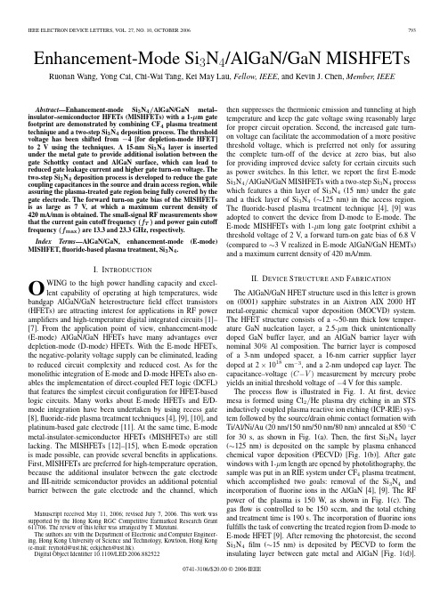
Enhancement-Mode Si3N4/AlGaN/GaN MISHFETs Ruonan Wang,Yong Cai,Chi-Wai Tang,Kei May Lau,Fellow,IEEE,and Kevin J.Chen,Member,IEEEAbstract—Enhancement-mode Si3N4/AlGaN/GaN metal–insulator–semiconductor HFETs(MISHFETs)with a1-µm gate footprint are demonstrated by combining CF4plasma treatment technique and a two-step Si3N4deposition process.The threshold voltage has been shifted from−4[for depletion-mode HFET] to2V using the techniques.A15-nm Si3N4layer is inserted under the metal gate to provide additional isolation between the gate Schottky contact and AlGaN surface,which can lead to reduced gate leakage current and higher gate turn-on voltage.The two-step Si3N4deposition process is developed to reduce the gate coupling capacitances in the source and drain access region,while assuring the plasma-treated gate region being fully covered by the gate electrode.The forward turn-on gate bias of the MISHFETs is as large as7V,at which a maximum current density of 420mA/mm is obtained.The small-signal RF measurements show that the current gain cutoff frequency(f T)and power gain cutoff frequency(f max)are13.3and23.3GHz,respectively.Index Terms—AlGaN/GaN,enhancement-mode(E-mode) MISHFET,fluoride-based plasma treatment,Si3N4.I.I NTRODUCTIONO WING to the high power handling capacity and excel-lent capability of operating at high temperatures,wide bandgap AlGaN/GaN heterostructurefield effect transistors (HFETs)are attracting interest for applications in RF power amplifiers and high-temperature digital integrated circuits[1]–[7].From the application point of view,enhancement-mode (E-mode)AlGaN/GaN HFETs have many advantages over depletion-mode(D-mode)HFETs.With the E-mode HFETs, the negative-polarity voltage supply can be eliminated,leading to reduced circuit complexity and reduced cost.As for the monolithic integration of E-mode and D-mode HFETs also en-ables the implementation of direct-coupled FET logic(DCFL) that features the simplest circuit configuration for HFET-based logic circuits.Many works about E-mode HFETs and E/D-mode integration have been undertaken by using recess gate [8],fluoride-ride plasma treatment techniques[4],[9],[10],and platinum-based gate electrode[11].At the same time,E-mode metal-insulator-semiconductor HFETs(MISHFETs)are still lacking.The MISHFETs[12]–[15],when E-mode operation is made possible,can provide several benefits in applications. First,MISHFETs are preferred for high-temperature operation, because the additional insulator between the gate electrode and III-nitride semiconductor provides an additional potential barrier between the gate electrode and the channel,whichManuscript received May11,2006;revised July7,2006.This work was supported by the Hong Kong RGC Competitive Earmarked Research Grant 611706.The review of this letter was arranged by T.Mizutani.The authors are with the Department of Electronic and Computer Engineer-ing,Hong Kong University of Science and Technology,Kowloon,Hong Kong (e-mail:reynold@ust.hk;eekjchen@ust.hk).Digital Object Identifier10.1109/LED.2006.882522then suppresses the thermionic emission and tunneling at high temperature and keep the gate voltage swing reasonably large for proper circuit operation.Second,the increased gate turn-on voltage can facilitate the accommodation of a more positive threshold voltage,which is preferred not only for assuring the complete turn-off of the device at zero bias,but also for providing improved device safety for certain circuits such as power switches.In this letter,we report thefirst E-mode Si3N4/AlGaN/GaN MISHFETs with a two-step Si3N4process which features a thin layer of Si3N4(15nm)under the gate and a thick layer of Si3N4(∼125nm)in the access region. Thefluoride-based plasma treatment technique[4],[9]was adopted to convert the device from D-mode to E-mode.The E-mode MISHFETs with1-µm long gate footprint exhibit a threshold voltage of2V,a forward turn-on gate bias of6.8V (compared to∼3V realized in E-mode AlGaN/GaN HEMTs) and a maximum current density of420mA/mm.II.D EVICE S TRUCTURE AND F ABRICATIONThe AlGaN/GaN HFET structure used in this letter is grown on(0001)sapphire substrates in an Aixtron AIX2000HT metal-organic chemical vapor deposition(MOCVD)system. The HFET structure consists of a∼50-nm thick low temper-ature GaN nucleation layer,a2.5-µm thick unintentionally doped GaN buffer layer,and an AlGaN barrier layer with nominal30%Al composition.The barrier layer is composed of a3-nm undoped spacer,a16-nm carrier supplier layer doped at2×1018cm−3,and a2-nm undoped cap layer.The capacitance–voltage(C−V)measurement by mercury probe yields an initial threshold voltage of−4V for this sample. The processflow is illustrated in Fig.1.Atfirst,device mesa is formed using Cl2/He plasma dry etching in an STS inductively coupled plasma reactive ion etching(ICP-RIE)sys-tem followed by the source/drain ohmic contact formation with Ti/Al/Ni/Au(20nm/150nm/50nm/80nm)annealed at850◦C for30s,as shown in Fig.1(a).Then,thefirst Si3N4layer (∼125nm)is deposited on the sample by plasma enhanced chemical vapor deposition(PECVD)[Fig.1(b)].After gate windows with1-µm length are opened by photolithography,the sample was put in an RIE system under CF4plasma treatment, which accomplished two goals:removal of the Si3N4and incorporation offluorine ions in the AlGaN[4],[9].The RF power of the plasma is150W,as shown in Fig.1(c).The gasflow is controlled to be150sccm,and the total etching and treatment time is190s.The incorporation offluorine ions fulfills the task of converting the treated region from D-mode to E-mode HFET[9].After removing the photoresist,the second Si3N4film(∼15nm)is deposited by PECVD to form the insulating layer between gate metal and AlGaN[Fig.1(d)].0741-3106/$20.00©2006IEEEFig. 1.Schematics showing the processflow of E-mode MISHFETs: (a)Active region and ohmic contact.(b)Thefirst Si3N4layer deposition.(c)Gate area definition and plasma treatment.(d)The second Si3N4layer deposition.(e)Si3N4patterned.(f)Schottky contact and interconnection. Subsequently,the Si3N4layer is patterned and etched to open windows in the source and drain ohmic contact regions,as shown in Fig.1(e).Next,the2-µm long gate electrodes are defined by photolithography followed by e-beam evaporation of Ni/Au(∼50nm/300nm)and liftoff[Fig.1(f)].To make sure the gate electrode covers the entire plasma-treated region,the metal gate length(2µm)is chosen to be larger than the treated gate area(1µm),leading to a T-gate configuration.The gate overhang in the source/drain access regions is insulated from the AlGaN layer by the thick Si3N4layer,keeping the gate capacitances at low level.At last,the whole sample is annealed at400◦C for10min to repair the plasma-induced damage in the AlGaN barrier and channel[4],[9].Measured from the foot of gate,the gate–source and gate–drain spacings are both 1.5µm.The E-mode MISHFETs are designed with gate width of10µm for dc testing and100µm for RF characterizations.III.D EVICE C HARACTERISTICSThe dc output characteristics of the E-mode MISHFETs are plotted in Fig.2.The devices exhibit a peak current density of∼420mA/mm,an ON-resistance of∼5.67Ω·mm and a knee voltage of∼3.3V at V GS=7V.Fig.3(a)shows the transfer characteristics of the same device with1×10-µm gate dimension.It can be seen that the threshold voltage V th is about 2V,indicating a6-V shift of V th(compared to a conventional D-mode HFET)achieved by the insertion of the Si3N4insu-lator and plasma treatment.The peak transconductance g m is ∼125mS/mm.Fig.3(b)shows the gate leakage current at both the negative bias and forward bias.The forward biasturn-on Fig.2.DC output characteristics of E-modeMISHFETs.Fig.3.(a)Transfer characteristics and(b)gate leakage current of E-mode MISHFETs.voltage for the gate is∼6.8V,providing a much larger gate bias swing compared to the E-mode HFETs[9].Pulse measurements were taken on the E-mode MISHFETs with1×100-µm gate dimensions with a pulse length of 0.2µS and a pulse separation of1mS.The quiescent bias point is chosen at V GS=0V(below V th)and V DS=20V.Fig.4 shows that the pulsed peak current is higher than the static one,indicating no current collapse in the device.The static maximum current density of the large device with a100-µm gate width is∼330mA/mm,smaller than the device with 10-µm gate width(∼420mA/mm).The lower peak current density in the larger device is due to the self-heating effect that lowers the current density.Since little self-heating occurs dur-ing pulse measurements,the maximum current for the100-µm wide device can reach the same level as the10-µm wide device. On wafer small-signal RF characteristics were performed from 0.1to39.1GHz on the100-µm wide E-mode MISHFETs at V DS=10V.As shown in Fig.5,the maximum current gain cutoff frequency(f T)and power gain cutoff frequency(f max)W ANG et al.:ENHANCEMENT-MODE Si 3N 4/AlGaN/GaN MISHFETs795Fig.4.Pulse measurements of E-modeMISHFETs.Fig.5.Small-signal RF characteristics of E-mode MISHFETs.are 13.3and 23.3GHz,respectively.When the gate bias is 7V ,the small-signal RF performance does not degrade much,with an f T of 13.1GHz and an f max of 20.7GHz,indicating that the Si 3N 4insulator offers an excellent insulation between gate metal and semiconductor.IV .C ONCLUSIONThe fabrication technology for E-mode AlGaN/GaN MISH-FET has been developed.The CF 4plasma treatment is used to convert D-mode devices to E-mode,shifting the threshold voltage from negative to positive.A two-step Si 3N 4deposition process is used to insert a thin layer of Si 3N 4as the gate insulating layer and create a thick layer between the gate electrode and the access region.The gate bias of the E-mode MISHFETs can be applied up to 7V .The E-mode MISHFETsshow no current collapse under pulse operation,and good dc and RF performances are obtained.R EFERENCES[1]V .Kumar,W.Lu,R.Schwindt,A.Kuliev,G.Simin,J.Yang,M.A.Khan,and I.Adesida,“AlGaN/GaN HEMTs on SiC with f T of over 120GHz,”IEEE Electron Device Lett.,vol.23,no.8,pp.455–457,Aug.2002.[2]Y .F.Wu,A.Saxler,M.Moore,R.P.Smith,S.Sheppard,P.M.Chavarkar,T.Wisleder,U.K.Mishra,and P.Parikh,“30-W/mm GaN HEMTs by field plate optimization,”IEEE Electron Device Lett.,vol.25,no.3,pp.117–119,Mar.2004.[3]J.W.Johnson,E.L.Piner,A.Vescan,R.Therrien,P.Rajagopal,J.C.Roberts,J.D.Brown,S.Singhal,and K.J.Linthicum,“12W/mm AlGaN-GaN HFETs on silicon substrates,”IEEE Electron Device Lett.,vol.25,no.7,pp.459–461,Jul.2004.[4]Y .Cai,Z.Q.Cheng,W.C.W.Tang,K.J.Chen,and u,“Mono-lithic integration of enhancement-and depletion-mode AlGaN/GaN HEMTs for GaN digital integrated circuits,”in IEDM Tech.Dig.,Dec.2005,pp.771–774.[5]I.Daumiller,C.Kirchner,M.Kamp,K.J.Ebeling,and E.Kohn,“Evalu-ation of the temperature stability of AlGaN/GaN heterostructure FET’s,”IEEE Electron Device Lett.,vol.20,no.9,pp.448–450,Sep.1999.[6]P.G.Neudeck,R.S.Okojie,and C.Liang-Yu,“High-temperatureelectronics—A role for wide bandgap semiconductors?,”Proc.IEEE ,vol.90,no.6,pp.1065–1076,Jun.2002.[7]T.Egawa,G.Y .Zhao,H.Ishikawa,M.Umeno,and T.Jimbo,“Character-izations of recessed gate AlGaN/GaN HEMTs on sapphire,”IEEE Trans.Electron Devices ,vol.48,no.3,pp.603–608,Mar.2003.[8]M.Micovic,T.Tsen,M.Hu,P.Hashimoto,P.J.Willadsen,osavljevic,A.Schmitz,M.Antcliffe,D.Zhender,J.S.Moon,W.S.Wong,and D.Chow,“GaN enhancement/depletion-mode FET logic for mixed signal applications,”Electron.Lett.,vol.41,no.19,pp.1081–1083,Sep.2005.[9]Y .Cai,Y .G.Zhou,K.J.Chen,and u,“High-performanceenhancement-mode AlGaN/GaN HEMTs using fluoride-based plasma treatment,”IEEE Electron Device Lett.,vol.26,no.7,pp.435–437,Jul.2005.[10]T.Palacios,C.-S.Suh,A.Chakraborty,S.Keller,S.P.DenBaars,andU.K.Mishra,“High-performance E-mode AlGaN/GaN HEMTs,”IEEE Electron Device Lett.,vol.27,no.6,pp.428–430,Jun.2006.[11]A.Endoh,Y .Yamashita,K.Ikeda,M.Higashiwaki,K.Hikosaka,T.Matsui,S.Hiyamizu,and T.Mimura,“Non-recessed-gate enhancement-mode AlGaN/GaN high electron mobility transistors with high RF performance,”Jpn.J.Appl.Phys.,vol.43,no.4B,pp.2255–2258,2004.[12]M.A.Khan,X.Hu,G.Sumin,A.Lunev,J.Yang,R.Gaska,and M.S.Shur,“AlGaN/GaN metal oxide semiconductor heterostructure field effect transistor,”IEEE Electron Device Lett.,vol.21,no.2,pp.63–65,Feb.2000.[13]X.Hu,A.Koudymov,G.Simin,J.Yang,and M.A.Khan,“Si 3N 4/AlGaN/GaN-metal-insulator-semiconductor heterostructure field-effect transistors,”Appl.Phys.Lett.,vol.79,no.17,pp.2832–2834,Oct.2001.[14]A.Chini,J.Wittich,S.Heikman,S.Keller,S.P.DenBaars,and U.K.Mishra,“Power and linearity characteristics of GaN MISFET on sap-phire substrate,”IEEE Electron Device Lett.,vol.25,no.2,pp.55–57,Feb.2004.[15]M.Kanamura,T.Kikkawa,T.Iwai,K.Imanishi,T.Kubo,and K.Joshin,“An over 100W n-GaN/n-AlGaN/GaN MIS-HEMT power amplifier for wireless base station applications,”in IEDM Tech.Dig.,Dec.2005,pp.572–575.。

hemt参数及测试方法English Answer:HEMT Parameters and Test Methods.The high-electron-mobility transistor (HEMT) is a typeof field-effect transistor (FET) that uses a heterojunction between two different semiconductor materials to create a high-mobility two-dimensional electron gas (2DEG) at the interface. HEMTs are known for their high electron mobility, low noise, and high power density, making them ideal foruse in high-frequency and high-power applications.The most important parameters of a HEMT are:Gate-source voltage (Vgs): The voltage applied between the gate and source terminals.Drain-source voltage (Vds): The voltage applied between the drain and source terminals.Gate-drain voltage (Vgd): The voltage applied between the gate and drain terminals.Drain current (Id): The current flowing from the drain to the source terminal.Source current (Is): The current flowing from the source to the drain terminal.Gate current (Ig): The current flowing from the gate to the source terminal.Transconductance (gm): The ratio of the change in drain current to the change in gate-source voltage.Output conductance (gds): The ratio of the change in drain current to the change in drain-source voltage.Input capacitance (Ciss): The capacitance between the gate and source terminals.Output capacitance (Coss): The capacitance between the drain and source terminals.Reverse transfer capacitance (Crss): The capacitance between the gate and drain terminals.These parameters can be measured using a variety of techniques, including:DC measurements: These measurements are made with a constant voltage applied to the gate-source terminal and a varying voltage applied to the drain-source terminal. The drain current, source current, and gate current are measured as the drain-source voltage is varied.AC measurements: These measurements are made with a small AC signal applied to the gate-source terminal and a constant voltage applied to the drain-source terminal. The transconductance, output conductance, input capacitance, output capacitance, and reverse transfer capacitance are measured as the frequency of the AC signal is varied.Pulsed measurements: These measurements are made with a pulsed voltage applied to the gate-source terminal and a constant voltage applied to the drain-source terminal. The drain current, source current, and gate current are measured as the pulse width and pulse repetition frequency are varied.The test methods used to measure HEMT parameters are constantly evolving as new technologies are developed. However, the basic principles of these methods remain the same.Chinese Answer:HEMT 参数及测试方法。
Front-End Electronics and Signal ProcessingHelmuth SpielerLawrence Berkeley National Laboratory, Physics Division, Berkeley, CA 94720, U.S.A.Abstract. Basic elements of front-end electronics and signal processing for radiation detectors are presented. The text covers system components, signal resolution, electronic noise and filtering, digitization, and some common pitfalls in practical systems.INTRODUCTIONElectronics are a key component of all modern detector systems. Although experiments and their associated electronics can take very different forms, the same basic principles of the electronic readout and optimization of signal-to-noise ratio apply to all. This paper provides a summary of front-end electronics components and discusses signal processing with an emphasis on electronic noise. Because of space limitations, this can only be a brief overview. The full course notes are available as pdf files on the world wide web [1]. More detailed discussions on detectors, signal processing and electronics are also available on the web [2].The purpose of front-end electronics and signal processing systems is to1.Acquire an electrical signal from the sensor. Typically this is a short current pulse.2. Tailor the time response of the system to optimizea) the minimum detectable signal (detect hit/no hit),b) energy measurement,c) event rate,d) time of arrival (timing measurement),e) insensitivity to sensor pulse shape,or some combination of the above.3. Digitize the signal and store for subsequent analysis.Position-sensitive detectors utilize the presence of a hit, amplitude measurement or timing, so these detectors pose the same set of requirements. Generally, these properties cannot be optimized simultaneously, so compromises are necessary.In addition to these primary functions of an electronic readout system, other considerations can be equally or even more important, for example, radiation resistance, low power (portable systems, large detector arrays, satellite systems), robustness, and – last, but not least – cost.Example SystemFig. 1 illustrates the components and functions in a radiation detector using a scintillation detector as an example. Radiation – in this example gamma rays – is absorbed in a scintillating crystal, which produces visible light photons. The number of scintillation photons is proportional to the absorbed energy. The scintillation photons are detected by a photomultiplier (PMT), consisting of a photocathode and an electron multiplier. Photons absorbed in the photocathode release electrons, where thenumber of electrons is proportional to the number of incident scintillation photons. At this point energy absorbed in the scintillator has been converted into an electrical signal whose charge is proportional to energy. The electron multiplier increases this signal charge by a constant factor. The signal at the PMT output is a current pulse.Integrated over time this pulse contains the signal charge, which is proportional to the absorbed energy. The signal now passes through a pulse shaper whose output feeds an analog-to-digital converter (ADC), which converts the analog signal into a bit-pattern suitable for subsequent digital storage and processing.If the pulse shape does not change with signal charge, the peak amplitude – the pulse height – is a measure of the signal charge, so this measurement is called pulse height analysis. The pulse shaper can serve multiple functions, which are discussed below. One is to tailor the pulse shape to the ADC. Since the ADC requires a finite time to acquire the signal, the input pulse may not be too short and it should have a gradually rounded peak. In scintillation detector systems the shaper is frequently an integrator and implemented as the first stage of the ADC, so it is invisible to the casual observer. Then the system appears very simple, as the PMT output is plugged directly into a charge-sensing ADC.INCIDENT RADIA TIONNUMBER OFSCINTILLATION PHOTONS PROP . ABS. ENERGY NUMBER OFPHOTO-ELECTRONS PROP . ABS. ENERGYCHARGE IN PUL PROP . ABS. ENESCINTILLATORPHOTOCATHODEELECTRON MULTIPLIERLIGHT ELECTRONSELECTRICAL SIGNALPHOTOMULTIPLIERPULSE SHAPINGANALOG TO DIGITAL CONVERSION DIGITAL DATA BUSFIGURE 1.Example detector signal processing chain.Detection Limits and ResolutionThe minimum detectable signal and the precision of the amplitude measurement are limited by fluctuations. The signal formed in the sensor fluctuates, even for a fixed energy absorption. Generally, sensors convert absorbed energy into signal quanta. In the scintillation detector shown as an example above, absorbed energy is converted into a number of scintillation photons. In an ionization chamber, energy is converted into a number of charge pairs (electrons and ions in gases or electrons and holes in solids). The absorbed energy divided by the excitation energy yields the average number of signal quanta /i N E H .This number fluctuates statistically, so the relative resolutionH '' i F E NFN E N N E.The resolution improves with the square root of energy. F is the Fano factor, which comes about because multiple excitation mechanisms can come into play and reduce the overall statistical spread. For example, in a semiconductor absorbed energy forms electron-hole pairs, but also excites lattice vibrations – quantized as phonons – whose excitation energy is much smaller (meV vs. eV). Thus,many more excitations are involved than apparent from the charge signal alone and this reduces the statistical fluctuations of the charge signal. For example, in Si the Fano factor is 0.1.In addition, electronic noise introduces baseline fluctuations, which are superimposed on the signal and alter the peak amplitude. Fig. 2 (left) shows a typical noise waveform. Both the amplitude and time distributions are random.When superimposed on a signal, the noise alters both the amplitude and time dependence. Fig. 2 (right) shows the noise waveform superimposed on a small signal.As can be seen, the noise level determines the minimum signal whose presence can be discerned.In an optimized system, the time scale of the fluctuations is comparable to that of the signal, so the peak amplitude fluctuates randomly above and below the average value. This is illustrated in Fig. 3, which shows the same signal viewed at four different times. The fluctuations in peak amplitude are obvious, but the effect of noise on timing measurements can also be seen. If the timing signal is derived from aTIME TIMEFIGURE 2.Waveforms of random noise (left) and signal + noise (right), where the peak signal isequal to the r.m.s. noise level (S /N = 1). The noiseless signal is shown for comparison.threshold discriminator, where the output fires when the signal crosses a fixed threshold, amplitude fluctuations in the leading edge translate into time shifts. If one derives the time of arrival from a centroid analysis, the timing signal also shifts (compare the top and bottom right figures). From this one sees that signal-to-noise ratio is important for all measurements – sensing the presence of a signal or the measurement of energy, timing, or position.ACQUIRING THE SENSOR SIGNALThe sensor signal is usually a short current pulse ()S i t . Typical durations vary widely, from 100 ps for thin Si sensors to tens of P s for inorganic scintillators.However, the physical quantity of interest is the deposited energy, so one has to integrate over the current pulse()v ³S S E Q i t dt .This integration can be performed at any stage of a linear system, so one can 1. integrate on the sensor capacitance,2. use an integrating preamplifier (“charge-sensitive” amplifier),3. amplify the current pulse and use an integrating ADC (“charge sensing” ADC),4. rapidly sample and digitize the current pulse and integrate numerically.In high-energy physics the first three options tend to be most efficient.TIME TIMETIME TIMEFIGURE 3.Signal plus noise at four different times. The signal-to-noise ratio is about 20 and thenoiseless signal is superimposed for comparison.Signal IntegrationFig. 4 illustrates signal formation in an ionization chamber connected to an amplifier with a very high input resistance. The ionization chamber volume could be filled with gas or a solid, as in a silicon sensor. As mobile charge carriers move towards their respective electrodes they change the induced charge on the sensor electrodes, which form a capacitor det C . If the amplifier has a very small input resistance i R , the time constant ()W i det i R C C for discharging the sensor is small,and the amplifier will sense the signal current. However, if the input time constant is large compared to the duration of the current pulse, the current pulse will be integrated on the capacitance and the resulting voltage at the amplifier inputSin det iQ V C C .The magnitude of the signal is dependent on the sensor capacitance. In a system with varying sensor capacitances, a Si tracker with varying strip lengths, for example, or a partially depleted semiconductor sensor, where the capacitance varies with the applied bias voltage, one would have to deal with additional calibrations. Although this is possible, it is awkward, so it is desirable to use a system where the charge calibration is independent of sensor parameters. This can be achieved rather simply with a charge-sensitive amplifier.Fig. 5 shows the principle of a feedback amplifier that performs integration. It consists of an inverting amplifier with voltage gain -A and a feedback capacitor C f connected from the output to the input. To simplify the calculation, let the amplifier have infinite input impedance, so no current flows into the amplifier input. If an input signal produces a voltage i v at the amplifier input, the voltage at the amplifier output is i Av . Thus, the voltage difference across the feedback capacitor (1)f i v A v and the charge deposited on C f is (1)f f f f i Q C v C A v . Since no current can flow intoR AMPLIFIERV inDETECTORC C idetivq t dq Q scs sttt dtVELOCITY OFCHARGE CARRIERSRATE OF INDUCED CHARGE ON SENSOR ELECTRODESSIGNAL CHARGEFigure 4. Charge collection and signal integration in an ionization chamberthe amplifier, all of the signal current must charge up the feedback capacitance, so f i Q Q . The amplifier input appears as a “dynamic” input capacitance (1)ii f iQ C C A v.The voltage output per unit input charge11(1)1o i Q i i i i f fdv Av A A A A dQ C v C A C C |!! ,so the charge gain is determined by a well-controlled component, the feedback capacitor. The signal charge S Q will be distributed between the sensor capacitance det C and the dynamic input capacitance i C . The ratio of measured charge to signal charge11i i idet s det s det iiQ Q C C Q Q Q C C C,so the dynamic input capacitance must be large compared to the sensor capacitance.C C C iTdetQ-AMPVTEST INPUTDYNAMIC INPUT CAPACITANCEFIGURE 6.Charge calibration circuitry of a charge-sensitive amplifierv Q C v iifo-ASENSORFIGURE 5.Basic configuration of a charge-sensitive amplifierAnother very useful byproduct of the integrating amplifier is the ease of charge calibration. By adding a test capacitor as shown in Fig. 6, a voltage step injects a well-defined charge into the input node. If the dynamic input capacitance i C is much larger than the test capacitance T C , the voltage step at the test input will be applied nearly completely across the test capacitance T C , thus injecting a charge T C V 'into the input.Realistic Charge-Sensitive AmplifiersThe preceding discussion assumed that the amplifiers are infinitely fast, that is that they respond instantaneously to the applied signal. In reality this is not the case;charge-sensitive amplifiers often respond much more slowly than the time duration of the current pulse from the sensor. However, as shown in Fig. 7, this does not obviate the basic principle. Initially, signal charge is integrated on the sensor capacitance, as indicated by the left hand current loop. Subsequently, as the amplifier responds the signal charge is transferred to the amplifier.Nevertheless, the time response of the amplifier does affect the measured pulse shape. First, consider a simple amplifier as shown in Fig. 8.The gain element shown is a bipolar transistor, but it could also be a field effect transistor (JFET or MOSFET) or even a vacuum tube. The transistor’s output current changes as the input voltage is varied. Thus, the voltage gainV +v i C R v iooL oFIGURE 8.A simple amplifierDETECTORC RAMPLIFIERi v i s indet inFIGURE 7.Realistic charge-sensitive amplifiero o V L m L i idv diA Z g Z dv dv {.The parameter m g is the transconductance, a key parameter that determines gain,bandwidth and noise of transistors. The load impedance L Z is the parallel combination of the load resistance L R and the output capacitance o C . This capacitance is unavoidable; every gain device has an output capacitance, the following stage has an input capacitance, and in addition the connections and additional components introduce stray capacitance. The load impedance is given by11o L LC Z R Z i ,where the imaginary i indicates the phase shift associated with the capacitance. The voltage gain11V m o L A g C R Z §·¨¸©¹i .At low frequencies where the second term is negligible, the gain is constant V m L A g R . However, at high frequencies the second term dominates and the gain falls off linearly with frequency with a 90q phase shift, as illustrated in Fig. 9. The cutoff frequency, where the asymptotic low and high frequency responses intersect, is determined by the output time constant L o R C , so the cutoff frequency12U L of R C S.In the regime where the gain drops linearly with frequency the product of gain and frequency is constant, so the amplifier can be characterized by its gain-bandwidth product, which is equal to the frequency where the gain is one, the unity gain frequency 0Z .The frequency response translates into a time response. If a voltage step is applied to the input of the amplifier, the output does not respond instantaneously, as the output capacitance must first charge up. This is shown in Fig. 10.log A log ZVg R R g 1m LL m-i Z C C ooupper cutoff frequency 2 S f uFIGURE 9.Frequency Response ofa simple amplifierINPUT OUTPUTOUTPUT : /(1)t o V V e W FIGURE 10.Pulse response of a simpleamplifierIn practice, amplifiers utilize multiple stages, all of which contribute to the frequency response. However, for use as a feedback amplifier, only one time constant should dominate, so the other stages must have higher cutoff frequencies. Then the overall amplifier response is as shown in Fig. 9, except that at high frequencies additional corner frequencies appear.We can now use the frequency response to calculate the input impedance and time response of a charge-sensitive amplifier. Applying the same reasoning as above, the input impedance of an amplifier as shown in Fig. 5, but with a generalized feedback impedance f Z , is(1)1ff iZ Z Z A A A|!! At low frequencies the gain is constant and has a constant 180q phase shift, so theinput impedance is of the samenature as the feedback impedance, but reduced by 1/A . At high frequencies well beyond the amplifier’s cutoff frequency U f , the gain drops linearly with frequency with an additional 90q phase shift, so the gain 0A Z Zi.In a charge-sensitive amplifier the feedback impedance 1f fZ C Z i,so the input impedance011iffZ C C Z Z Z Zi i .The imaginary component vanishes, so the input impedance is real. In other words, it appears as a resistance. Thus, at low frequencies U f f the input of a charge-sensitive amplifier appears capacitive, whereas at high frequencies U f f !it appears resistive.Suitable amplifiers invariably have corner frequencies well below the frequencies of interest for radiation detectors, so the input impedance is resistive. This allows a simple calculation of the time response. The sensor capacitance is discharged by the resistive input impedance of the fedback amplifier with the time constant01i i det det fR C C C W Z.From this we see that the rise time of the charge-sensitive amplifier increases with sensor capacitance. As noted above, the amplifier response can be slower than the duration of the current pulse from the sensor, but it should be much faster than the peaking time of the subsequent pulse shaper. For reasons that will become apparent later, the feedback capacitance should be much smaller than the sensor capacitance. If /100f det C C , the amplifier’s gain-bandwidth product must be 100/i W , so for a rise time constant of 10ns the gain-bandwidth product must be 1010radians = 1.6GHz.The same result can be obtained using conventional operational amplifier feedback theory.Apart from determining the signal rise time, the input impedance is critical in position-sensitive detectors. Fig. 11 illustrates a silicon-strip sensor read out by a bank of amplifiers. Each strip electrode has a capacitance SG C to the backplane and a fringing capacitance SS C to the neighboring strips. If the amplifier has an infinite input impedance, charge induced on one strip will capacitively couple to the neighbors and the signal will be distributed over many strips (determined by /SS SG C C ). If, on the other hand, the input impedance of the amplifier is low compared to the inter-strip impedance 1//SS i SS C C Z W |, practically all of the charge will flow into the amplifier,as current seeks the path of least impedance,and the neighbors will show only a small signal.SIGNAL PROCESSINGAs noted in the introduction, one of the purposes of signal processing is to improve the signal-to-nose ratio by tailoring the spectral distributions of the signal and the electronic noise. However, for many detectors electronic noise does not determine the resolution. For example, in a NaI(Tl) scintillation detector measuring 511keV gamma rays, say in a positron-emission tomography system, 25000 scintillation photons are produced. Because of reflective losses, about 15000 reach the photocathode. This translates to about 3000 electrons reaching the first dynode. The gain of the electron multiplier will yield about 3 109electrons at the anode. The statistical spread of the signal is determined by the smallest number of electrons in the chain, i.e. the 3000electrons reaching the first dynode, so the resolution /1/30002%E E ', which at the anode corresponds to about 5 104electrons.This is much larger than electronic noise in any reasonably designed system. This situation is illustrated in Fig. 12 (top).In this case, signal acquisition and count rate capability may be the prime objectives ofFIGURE 11.Cross coupling in a silicon strip sensorthe pulse processing system. The bottom illustration in Fig. 12 shows the situation for high resolution sensors with small signals, for example semiconductor detectors,photodiodes or ionization chambers. In this case, low noise is critical. Baseline fluctuations can have many origins, external interference, artifacts due to imperfect electronics, etc., but the fundamental limit is electronic noise.Electronic NoiseConsider a current flowing through a sample bounded by two electrodes, i.e. n electrons moving with velocity v . The induced current depends on the spacing l between the electrodes (see “Ramo’s theorem” in ref. 7), so nevi l.The fluctuation of this current is given by the total differential222ne ev didv dn l l §·§·¨¸¨¸©¹©¹,where the two terms add in quadrature, as they are statistically uncorrelated. From this one sees that two mechanisms contribute to the total noise, velocity and number fluctuations.Velocity fluctuations originate from thermal motion. Superimposed on the average drift velocity are random velocity fluctuations due to thermal excitations. ThisSIGNALBASELINE NOISE SIGNAL +NOISE+BASELINE BASELINE BASELINESIGNALBASELINE NOISE SIGNAL +NOISE+BASELINE BASELINE BASELINEFIGURE 12. Signal and baseline fluctuations for large signal variance (top), as in scintillation detectors or proportional chambers, and for small signal variance, but large baseline fluctuations,as in semiconductor detectors or liquid Ar ionization chambers, for example.“thermal noise” is described by the long wavelength limit of Planck’s black body spectrum where the spectral density, i.e. the power per unit bandwidth, is constant (“white” noise).Number fluctuations occur in many circumstances. One source is carrier flow that is limited by emission over a potential barrier. Examples are thermionic emission or current flow in a semiconductor diode. The probability of a carrier crossing the barrier is independent of any other carrier being emitted, so the individual emissions are random and not correlated. This is called “shot noise”, which also has a “white”spectrum. Another source of number fluctuations is carrier trapping. Imperfections in a crystal lattice or impurities in gases can trap charge carriers and release them after a characteristic lifetime. This leads to a frequency-dependent spectrum /1/n dP df f D ,where D is typically in the range of 0.5 to 2.Thermal (Johnson) NoiseThe most common example of noise due to velocity fluctuations is the noise of resistors. The spectral noise density vs. frequency4ndP kT dfwhere k is the Boltzmann constant and T the absolute temperature. Since the power in a resistance R22V P I R R,the spectral voltage noise density224n n dV e kTR df{ and the spectral current noise density224n n dI kT i df R{ .The total noise is obtained by integrating over the relevant frequency range of thesystem, the bandwidth. The total noise voltage at the output of an amplifier with a frequency-dependent gain ()A f is222()onn v e A f df f³.Since the spectral noise components are non-correlated (each black body excitation mode is independent), one must integrate over the noise power, i.e. the voltage squared. The total noise increases with bandwidth. Since small bandwidth corresponds to large rise-times, increasing the speed of a pulse measurement system will increase the noise. The amplitude distribution of the noise is Gaussian, so noise fluctuations superimposed on the signal also yield a Gaussian distribution. Thus, by measuring the width of the amplitude spectrum of a well-defined signal, one can determine the noise.Shot NoiseThe spectral noise density of shot noise is proportional to the average current I22n e i q I ,where e q is the electronic charge. Note that the criterion for shot noise is that carriers are injected independently of one another, as in thermionic or semiconductor diodes.Current flowing through an ohmic conductor does not carry shot noise, since the fields set up by any local fluctuation in charge density can easily draw in additional carriers to equalize the disturbance.Signal-to-Noise Ratio vs. Sensor CapacitanceThe basic noise sources manifest themselves as either voltage or current fluctua-tions. However, the desired signal is a charge, so to allow a comparison we must express the signal as a voltage or current. This was illustrated for an ionization chamber in Fig. 5. As was noted, when the input time constant ()in det in R C C is large compared to the duration of the sensor current pulse, the signal charge is integrated on the input capacitance, yielding the signal voltage /()S S det in v Q C C . Assume that the amplifier has an input noise voltage n v . Then the signal-to-noise ratio()S Sn n det in v Q v v C C.This is a very important result, i.e. the signal-to-noise ratio for a given signal charge is inversely proportional to the total capacitance at the input node. Note that zero input capacitance does not yield an infinite signal-to-noise ratio. As shown in Appendix 4 of the original course notes [1], this relationship only holds when the input time constant is greater than about ten times the sensor current pulse width. This is a general feature that is independent of amplifier type. Since feedback cannot improve signal-to-noise ratio, it also holds for charge-sensitive amplifiers, although in that configuration the charge signal is constant, but the noise increases with total input capacitance (see ref.1). In the noise analysis the feedback capacitance adds to the total input capacitance (not the dynamic input capacitance!), so f C should be kept small.Pulse ShapingPulse shaping has two conflicting objectives. The first is to restrict the bandwidth to match the measurement time. Too large a bandwidth will increase the noise without increasing the signal. Typically, the pulse shaper transforms a narrow sensor pulse into a broader pulse with a gradually rounded maximum at the peaking time. This is illustrated in Fig. 13. The signal amplitude is measured at the peaking time P T .The second objective is to constrain the pulse width so that successive signal pulses can be measured without overlap (pileup), as illustrated in Fig. 14. Reducing the pulse duration increases the allowable signal rate, but at the expense of electronic noise.In designing the shaper it is necessary to balance these conflicting goals. Usually,many different considerations lead to a “non-textbook” compromise; “optimum shaping” depends on the application.A simple shaper is shown in Fig. 15. A high-pass filter sets the duration of the pulse by introducing a decay time constant d W . Next a low-pass filter increases the rise time to limit the noise bandwidth. The high-pass is often referred to as a “differentiator”,since for short pulses it forms the derivative. Correspondingly, the low-pass is called an “integrator”. Since the high-pass filter is implemented with a CR section and the low-pass with an RC , this shaper is referred to as a CR-RC shaper. Although pulse shapers are often more sophisticated and complicated, the CR-RC shaper contains the essential features of all pulse shapers, a lower frequency bound and an upper frequency bound.Noise Analysis of a Detector and Front-End AmplifierTo determine how the pulse shaper affects the signal-to-noise ratio consider the detector front-end in Fig. 16. The detector is represented by a capacitance, a relevant model for many radiation sensors. Sensor bias voltage is applied through the resistor B R . The bypass capacitor B C shunts any external interference coming through the bias supply line to ground. For high-frequency signals this capacitor appears as a low impedance, so for sensor signals the “far end” of the bias resistor is connected toT PSENSOR PULSE SHAPER OUTPUTFIGURE 13. A pulse shaper transforms a short sensor pulse into alonger pulse with a rounded cusp and peaking time T P .TIMEA M P L I T U D ETIMEA M P L I T U D EFIGURE 14. Amplitude pileup when two successive pulses overlap (left). Reducing the shaping timeallows the first pulse to return to the baseline before the second arrives.ground. The coupling capacitor C C blocks the sensor bias voltage from the amplifier input, which is why a capacitor serving this role is also called a “blocking capacitor”.The series resistance S R represents any resistance present in the connection from the sensor to the amplifier input. This includes the resistance of the sensor electrodes, the resistance of the connecting wires or traces, any resistance used to protect the amplifier against large voltage transients (“input protection”), and parasitic resistances in the input transistor.The following implicitly includes a constraint on the bias resistance, whose role is often misunderstood. It is often thought that the signal current generated in the sensor flows through b R and the resulting voltage drop is measured. If the time constant b d R C is small compared to the peaking time of the shaper P T , the sensor will have discharged through b R and much of the signal will be lost. Thus, we have the condition b d P R C T !!, or /b P D R T C !!. The bias resistor must be sufficiently large to block the flow of signal charge, so that all of the signal is available for the amplifier.OUTPUTDETECTORBIASRESISTORR bC c R sC bC dDETECTOR BIASPULSE SHAPERPREAMPLIFIERFIGURE 16. A typical detector front-end circuit99d iHIGH-PASS FILTER “DIFFERENTIATOR”LOW-PASS FILTER “INTEGRATOR”e -t /9dFIGURE 15. A simple pulse shaper using a CR “differentiator” as a high-pass and an RC“integrator” as a low-pass filter.。
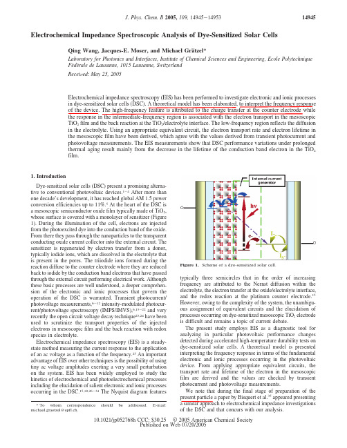
Electrochemical Impedance Spectroscopic Analysis of Dye-Sensitized Solar CellsQing Wang,Jacques-E.Moser,and Michael Gra1tzel*Laboratory for Photonics and Interfaces,Institute of Chemical Sciences and Engineering,Ecole PolytechniqueFe´de´rale de Lausanne,1015Lausanne,SwitzerlandRecei V ed:May25,2005Electrochemical impedance spectroscopy(EIS)has been performed to investigate electronic and ionic processesin dye-sensitized solar cells(DSC).A theoretical model has been elaborated,to interpret the frequency responseof the device.The high-frequency feature is attributed to the charge transfer at the counter electrode whilethe response in the intermediate-frequency region is associated with the electron transport in the mesoscopicTiO2film and the back reaction at the TiO2/electrolyte interface.The low-frequency region reflects the diffusionin the ing an appropriate equivalent circuit,the electron transport rate and electron lifetime inthe mesoscopic film have been derived,which agree with the values derived from transient photocurrent andphotovoltage measurements.The EIS measurements show that DSC performance variations under prolongedthermal aging result mainly from the decrease in the lifetime of the conduction band electron in the TiO2film.1.IntroductionDye-sensitized solar cells(DSC)present a promising alterna-tive to conventional photovoltaic devices.1-4After more thanone decade’s development,it has reached global AM1.5powerconversion efficiencies up to11%.5At the heart of the DSC isa mesoscopic semiconductor oxide film typically made of TiO2,whose surface is covered with a monolayer of sensitizer(Figure1).During the illumination of the cell,electrons are injectedfrom the photoexcited dye into the conduction band of the oxide.From there they pass through the nanoparticles to the transparentconducting oxide current collector into the external circuit.Thesensitizer is regenerated by electron transfer from a donor,typically iodide ions,which are dissolved in the electrolyte thatis present in the pores.The triiodide ions formed during thereaction diffuse to the counter electrode where they are reducedback to iodide by the conduction band electrons that have passed through the external circuit performing electrical work.Although these basic processes are well understood,a deeper comprehen-sion of the electronic and ionic processes that govern the operation of the DSC is warranted.Transient photocurrent/ photovoltage measurements,6-12intensity-modulated photocur-rent/photovoltage spectroscopy(IMPS/IMVS),6,13-22and very recently the open circuit voltage decay technique23,24have been used to scrutinize the transport properties of the injected electrons in mesoscopic film and the back reaction with redox species in electrolyte.Electrochemical impedance spectroscopy(EIS)is a steady-state method measuring the current response to the application of an ac voltage as a function of the frequency.25An important advantage of EIS over other techniques is the possibility of using tiny ac voltage amplitudes exerting a very small perturbation on the system.EIS has been widely employed to study the kinetics of electrochemical and photoelectrochemical processes including the elucidation of salient electronic and ionic processes occurring in the DSC.15,18,26-34The Nyquist diagram features typically three semicircles that in the order of increasing frequency are attributed to the Nernst diffusion within the electrolyte,the electron transfer at the oxide/electrolyte interface, and the redox reaction at the platinum counter electrode.15 However,owing to the complexity of the system,the unambigu-ous assignment of equivalent circuits and the elucidation of processes occurring on dye-sensitized mesoscopic TiO2electrode is difficult and remains a topic of current debate.The present study employs EIS as a diagnostic tool for analyzing in particular photovoltaic performance changes detected during accelerated high-temperature durability tests on dye-sensitized solar cells.A theoretical model is presented interpreting the frequency response in terms of the fundamental electronic and ionic processes occurring in the photovoltaic device.From applying appropriate equivalent circuits,the transport rate and lifetime of the electron in the mesoscopic film are derived and the values are checked by transient photocurrent and photovoltage measurements.We note that during the final stage of preparation of the present particle a paper by Bisquert et al.35appeared presenting a similar approach to electrochemical impedance investigations of the DSC and that concurs with our analysis.*To whom correspondence should be addressed.E-mail:michael.graetzel@epfl.ch.Figure1.Scheme of a dye-sensitized solar cell.14945 J.Phys.Chem.B2005,109,14945-1495310.1021/jp052768h CCC:$30.25©2005American Chemical SocietyPublished on Web07/20/20052.Theoretical Modeling of the Frequency ResponseThe DSC contains three spatially separated interfaces formed by FTO/TiO2,TiO2/electrolyte,and electrolyte/Pt-FTO.Elec-tron transfer is coupled to electronic and ionic transport.In the dark under forward bias electrons are injected in the conduction band of the nanoparticles and their motion is coupled to that of I-/I3-ions in electrolyte.Illumination gives rise to new redox processes at the TiO2/dye/electrolyte interface comprising sensitized electron injection,recombination with the parent dye, and regeneration of the sensitizer.During photovoltaic operation, this“internal current generator”drives all the electronic and ionic processes in the solar cell.31We now derive the equations describing the frequency response of the impedance at the different interfaces.2.1.I3-Finite Diffusion within Electrolyte and Electron Transfer at the Pt-FTO/Electrolyte Interface.In practical electrolytes,the concentration of triiodide is much lower than that of iodide and the latter is diffuses faster than the former ion.Hence,I-contributes little to the overall diffusion imped-ance,which is determined by the motion of I3-.The diffusion of I3-within a thin layer cell is well described by a Nernst diffusion impedance Z N.15,28Using Fick’s law and appropriate boundary conditions Z N becomeswhereωis the angular frequency and R equals0.5for a finite length Warburg impedance(FLW).Z0andτd are the Warburg parameter and characteristic diffusion time constant,respec-tively,which can be expressed bywhere R is the molar gas constant,T the temperature,F the Faraday constant,c0the bulk concentration of I3-,A the electrode area,D the diffusion coefficient of I3-,and d is the diffusion length.Because of the mesoporous character of the TiO2electrode,a modified Nernst diffusion impedance with R deviating from0.5is used to fit the transport of I3-.Nernst diffusion impedance in the Nyquist plot shows typically a straight line at higher frequency along with a semicircle at lower frequency.Fitting Z0andτd,the diffusion coefficient can be determined.The charge-transfer resistance R CT associated with the heterogeneous electron exchange involving the I3-T I-redox couple at the electrolyte/Pt-FTO interface is typically given for the equilibrium potential.From the Bulter-Volmer equation, one obtainswhere i0is the exchange current density of the reaction.The frequency response of charge-transfer impedance under small sinusoidal perturbation can be expressed as36where C d is the double layer capacitance.The charge-transfer resistance manifests itself as a semicircle in the Nyquist diagram and a peak in the Bode phase angle plot.For electrodes having a rough surface the semicircle is flattened and C d is replaced by a constant phase element(CPE).2.2.Electron Transport within the Mesoscopic TiO2Film and Electron Loss due to the Reduction of Triiodide at the TiO2/Electrolyte Interface.When a voltage modulation is applied in the dark to the mesoporous TiO2electrode of the DSC,electrons are injected and recovered during the cathodic and anodic parts of the current response.Their collection yield of recollecting the injected electrons depends on their diffusion lengthwhere D e is the diffusion coefficient andτr the lifetime of the electron within the film.The impedance due to electron diffusion and loss by the interfacial redox reaction in a thin mesoporous layer has been treated by Bisquert.31-34For the case of a mesoscopic TiO2film, the diffusion occurs over a finite length and is coupled with interfacial electron-transfer reaction.The electron charge is screened by the electrolyte,which eliminates the internal field, so no drift term appears in the transport equation.4The continuity equation contains therefore only the diffusion and reaction terms. the boundary condition beingwhere n is the concentration of electron,n0is their initial concentration,and L is the film thickness.To account for a harmonically modulated voltage,a frequency term is introduced yielding finally for the impedance response:where R d and R r are the diffusion and dark reaction impedance, respectively,whileωd′(ωd′)1/τd′)D e/L2)andωr(ωr)1/τr) are the corresponding characteristic frequencies.If R r f∞,eq 9describes a simple diffusion process within restricted bound-aries.For a DSC exhibiting a current collection efficiency close to unity,the condition R r.R d applies and eq9becomesUnder these conditions,the Nyquist plot shows a short straight line at higher frequencies due to diffusion and a large semicircle in the lower frequency regime,indicating fast electron transport and long lifetime of electron in the film.By contrast,if the electron collection efficiency is low,i.e.,a major part of the electron reacts with I3-in the electrolyte before they are recovered at the current collector,the condition R d.R r applies leading to Gerischer impedance34,37Z N )Z(iω)Rtanh(iτdω)R(1)Z)RTn2F2cA D(2)τd)d2/D(3)RCT)RTnF1i0(4)Z)iRCTi-RCTCdω(5)Ln) D eτr(6)∂n∂t)De∂2n∂x2-(n-n)τr(7)∂n∂x|x)L)0(8)Z)(R d R r1+iω/ωr)1/2coth[(ωr/ωd′)1/2(1+iω/ωr)1/2](9)Z)13Rd+Rr1+iω/ωr(Rr.Rd)(10)Z)(R d R r1+iω/ωr)1/2(R d.R r)(11)14946J.Phys.Chem.B,Vol.109,No.31,2005Wang et al.The Gerischer impedance produces response curves similar to a FLW impedance (eq 1).It shows a Warburg diffusion-like straight line at higher frequencies along with a semicircle at lower frequencies.The diffusion coefficient D e and the lifetime τr of the electron in the film can be obtained from eqs 10and 11.The above discussion was based on DSC in the dark and under forward bias.Under illumination the continuity equation becomeswhere R ′is the effective absorption coefficient,ηinj is thequantum yield for charge injection,and I is the incident photon flux,the boundary condition being again given by eq 8.As indicated in Figure 2,under illumination the short circuit photocurrent J SC of the cell iswhere J inj is the flux of injected electron and J loss is the current from back reaction loss.Since ηcc )1for distances x <L n ,and ηcc )0if x >L n ,where J inj,x <Ln is the anodic flux of electron that are injected by the sensitizer and collected at the FTO,while J FTO -TiO 2is the cathodic current flowing from the FTO into the TiO 2film.Thus,where J inj,x >Ln is the flux of injected electron,which is lost completely before arriving at FTO/TiO 2interface.It is clear that J inj,x <Ln <J FTO -TiO 2as E >V OC (Figure 2a);and J inj,x <Ln >J FTO -TiO 2as E <V OC (Figure 2c).At open circuit state (Figure 2b),J inj ,x <Ln equals to J FTO -TiO 2,and the total flux is zero.Phenomenologically we can treat the perturbation imposed by the illumination as if a voltage bias was applied in the dark.This applies in particular for a situation where the diffusion length of the electrons is commensurate with or larger than the film thickness.Hence,the same approach as above can be used to analyze its frequency response.Nevertheless,the model may overstate the diffusion rate D e because photons travel through the film faster than conduction band electrons.But the correction is small if the electrondiffusion length is long compared to the film thickness L .31Indeed,as will be shown below,in a DSC L n normally exceeds L rendering this distinction irrelevant.2.3.Equivalent Circuits and Typical Impedance Spectra of DSC.For a nanoporous electrode,the infinite transmission line is normally used as the equivalent circuit for modeling.For simplicity,only the representative elements displayed in Figure 3are employed here to model DSC at different states.From left to right,Figure 3shows the electron transport at the FTO/TiO 2interface,electron transport and electron capture by the I 3-at the TiO 2/electrolyte interface,diffusion of I 3-in the electrolyte,and charge transfer at electrolyte/Pt -FTO interface,respectively.For a cell exhibiting a carrier collection efficiency near unity,the condition R r .R d and eq 10applies.In this case,the equivalent circuit for the mesoporous TiO 2film comprises a diffusion element Z W1that is in series connected with the charge-transfer element R REC ,the two being in parallel with a capacitive (constant phase angle)element CPE3,as shown in Figure 3a.On the other hand,for cells where only a fraction of the photogenerated charge carriers are collected,the condition of R d .R r applies and a single Gerischer impedance element Z G describes the diffusion of the electron in the mesoscopic TiO 2film and their recapture by the triiodide ions in the electrolyte (Figure 3b).R FTO/TiO 2is the resistance of the FTO/TiO 2contact and CPE1is the capacitance of this interface.The latter feature,due to overlap with other processes,is not easily distinguished.Z W2is the Warburg impedance describing the diffusion of I 3-in the electrolyte,R CE is thecharge-transferFigure 2.Schematic model of photoanode at different voltages.(a)E >V OC ;(b)E )V OC ;(c)E <V OC .L is the film thickness,L n is the electron effective diffusion length,and ηcc is the charge collection efficiency of injected electron.∂n ∂t)R ′I ηinj +D e ∂2n ∂x2-(n -n 0)τr (12)J SC )J inj -J loss(13)J SC )J inj,x <L n -J FTO -TiO 2(14)J loss )J inj,x >L n +J FTO -TiO 2(15)Figure 3.Equivalent circuits of DSC.(a)a cell showing quantitative collection of photoinjected electrons;(b)a cell showing incomplete collection of electrons.Bottom line shows the interpretation of the electrical elements of the equivalent circuit.(A)electron transfer at the FTO/TiO 2interface;(B)electron transport and back reaction at the mesoscopic TiO 2/electrolyte interface;(C)diffusion of I 3-in the electrolyte;(D)charge at electrolyte/Pt -FTO interface.Dye-Sensitized Solar Cell J.Phys.Chem.B,Vol.109,No.31,200514947impedance at the counter electrode,and CPE2is the double layer capacitance at the electrolyte/Pt -FTO interface.A typical EIS spectrum for a DSC exhibits three semicircles in the Nyquist plot or three characteristic frequency peaks in a Bode phase plot.This is illustrated in Figure 4showing Nyquist plots of a N719sensitized DSC before and after thermal aging at 80°C for 2days.The response in the intermediate-frequency regime changes greatly upon aging,indicating the conversion of a Nernst to a Gerischer impedance.Apparently,the spectra can be well fitted in terms of the corresponding equivalent circuits in Figure 3.These models will therefore be employed to interpret impedance data in the following sections.3.Experimental Section3.1.Dye-Sensitized Mesoscopic TiO 2Electrode Prepara-tion and Cell Fabrication.The preparation of mesoscopic TiO 2film has been described in ref 38.The screen-printed double-layer film consists of a 10-µm transparent layer and a 4-µm scattering layer whose thickness was determined by using an Alpha-step 200surface profilometer (Tencor Instruments).A porosity of 0.63for the transparent layer was measured with a Gemini 2327nitrogen adsorption apparatus (Micromeretics Instrument Corp.).The film was heated to 500°C in air and calcinated for 20min before use.Then the still hot spots were dipped into a 2×10⁻⁴M 2-fold deprotonated cis-RuL2(SCN)2(L )2,2′-bipyridyl-4,4′-dicarboxylic acid)(N719)or cis-RuLL ′-(SCN)2(L )2,2′-bipyridyl-4,4′-dicarboxylic acid,L ′)4,4′-dinonyl-2,2′-bipyridyl)(Z907)dye (Chart 1)solution in aceto-nitrile/tert -butyl alcohol (1:1)and left for overnight.Finally,the dye-coated electrodes were rinsed with acetonitrile.For transient photocurrent/photovoltage measurements,single trans-parent TiO 2films with the thickness of 12µm were used.A sandwich cell was prepared using the dye-sensitized electrode as the working electrode and a platinum-coated conducting glass electrode as the counter electrode.The latter was prepared by chemical deposition of platinum from 0.05M hexachloroplatinic acid at 400°C.The two electrodes were placed on top of each other using a thin transparent film of Bynel polymer (DuPont)as a spacer.The empty cell was tightly held,and the edges were heated to 130°C in order to seal the two electrodes together.A thin layer of electrolyte was introduced into the interelectrode space from the counter electrode side through a predrilled hole.The hole was sealed with a microscope cover slide and Bynel to avoid leakage of the electrolyte solution.There were two electrolytes used in this paper:electrolyte 1,0.6M PMII,0.1M I 2,and 0.5M NMB in MPN;electrolyte 2,0.6M DMPII,0.05M I 2,0.5M tBuPy,0.1M LiI in AN:VN(1:1).Thermal stress tests were carried out by putting cells in an oven at 80°C and then measuring the I -V curve,impedance and transient photocurrent/photovoltage.3.2.I -V Measurements.A 450-W xenon light source (Osram XBO 450)was used as the irradiation source for the I -V measurements.The spectral output of the lamp matched the AM 1.5solar spectrum in the region of 350-750nm (mismatch <2%).Incident light intensities were adjusted with neutral wire mesh attenuators.The current -voltage character-istics were determined by applying an external potential bias to the cell and measuring the photocurrent using a Keithley model 2400digital source meter (Keithley).The overall conversion efficiency ηof the photovoltaic cell is calculated from the integral photocurrent density (J SC ),the open-circuit photovoltage (V OC ),the fill factor of the cell (ff),and the intensity of the incident light (I Ph ),3.3.Electrochemical Impedance Measurements.Impedance measurements were performed with acomputer-controlledFigure 4.Typical Nyquist plots of a N719sensitized DSC.Filled squares,fresh cell;open circles,cell after aging for 48h at 80°C.The lines show theoretical fits using the equivalent circuits shown in Figure 3a and b,respectively.The electrolyte is 0.6M PMII,0.1M I 2,and 0.5M NMB in MPN.CHART 1:Sensitizers Used in This StudyaaKey:(a)N719;(b)Z907.η)J SC ‚V OC ‚ff/I Ph(16)14948J.Phys.Chem.B,Vol.109,No.31,2005Wang et al.potentiostat(EG&G,M273)equipped with a frequency response analyzer(EG&G,M1025).The frequency range is0.005-100 kHz.The magnitude of the alternative signal is10mV.Unless otherwise mentioned,all impedance measurements were carried out under a bias illumination of100mW/cm2(global AM1.5, 1sun)from a450-W xenon light source.The obtained spectra were fitted with Z-View software(v2.1b,Scribner Associate, Inc.)in terms of appropriate equivalent circuits.3.4.Transient Photocurrent/Photovoltage Measurements. Transient photocurrent and photovoltage studies of the DSC were carried out by using weak laser pulses atλ)514nm, superimposed on a relatively intense bias illumination.The bias light was supplied by a cw450-W Xe arc lamp,equipped with a water filter and a680-nm cutoff filter.The continuous wave beam was condensed by a lens to irradiate a∼1cm2cross section of the cell,the surface of which was kept at a60°angle to the beam.The red light intensity measured at the cell position was typically120mW/cm2.The cell was oriented to expose the counter electrode side to both the bias light and laser beams. The5-ns-duration laser pulses at a wavelength of514nm were generated by a broadband optical parametric oscillator(GWU,OPO-355)pumped by the third harmonic of a30-Hz repetition rate,Q-switched Nd:YAG laser(Continuum,Powerlite7030). The laser beam was attenuated by gray filters to restrict the pulse fluence onto the cell to<100µJ/cm2.The514-nm laser light was strongly absorbed by the dye,and therefore,injected electrons were introduced into a narrow spatial region,corre-sponding to where the probe light enters the film.Current transients were measured across a20Ωresistor load using a large bandwidth digital signal analyzer(Tektronix DSA602A). Transient photovoltages were measured by feeding the signal directly into the DSA amplifier,whose impedance was1MΩ.4.Results and Discussion4.1.Impedances of DSC Obtained in Dark and Illumina-tion.There are different processes that occur in the cell in the dark or under illumination.At open circuit voltage and in sunlight,there is no net current flowing through the cell.All the injected electrons are recaptured by I3-before being extracted to the external circuit.Meanwhile,the oxidized dye is regenerated by I-.As a result,the absorbed photon energy is converted to heat through the two coupled redox cycles involving sensitized electron injection,dye regeneration,and electron recapture by I3-.The counter electrode is kept at equilibrium,because there is no net current flowing through it. However,in the dark under forward bias,electrons are transported through the mesoscopic TiO2network and react with I3-.At the same time,I-is oxidized to I3-at the counter electrode.The net current density can be large depending on the applied bias voltage.Figure5shows the impedance spectra of a DSC measured at OCV(-0.68V)under1sun and under forward bias(-0.68 V)in the dark.Strikingly,the impedance due to electron transfer from the conduction band of the mesoscopic film to triiodide ions in the electrolyte,presented by the semicircle in intermedi-ate-frequency regime,is much smaller under light than in the dark even though the potential of the film is the same. Correspondingly,the characteristic frequency shown in Bode phase plots increases two times,suggesting the electron lifetime is shortened by a factor of2.This can be ascribed to a difference in the local I3-concentration.Under illumination,I3-is formed “in situ”by dye regeneration at the mesoporous TiO2/electrolyte interface,whereas in the dark,I3-is generated at counter electrode and penetrates the mesoporous TiO2films by diffusion.As indicated by eq17,the higher local I3-concentrationproduced in the porous network under light is expected toaccelerate the recapture of conduction band electrons andshortens their lifetime within the TiO2film.Here J r is the I3-reduction current,k r is the rate constant of thereduction reaction,and c ox is the concentration of I3-;theexponentsγand are the reaction orders for I3-and electrons,respectively.4.2.Impedance of DSC with Different Electrolytes.Electrolytes exert a great influence on the photovoltaic perfor-mance of the DSC by effecting the kinetics of electronic or ionicprocesses.For instance,acetonitrile(AN)-based electrolytes havemuch lower viscosity compared with3-methoxypropionitrile(MPN),the kinetics of dye regeneration,I3-f I-reaction at counter electrode,electron transport within the TiO2film,andI-/I3-diffusion in electrolyte being faster in the former case.Consequently,much better photovoltaic performance has beenachieved.In addition,additives in the electrolyte are of greatimportance for optimization and stabilization of the TiO2/dye/electrolyte interface.TBP,39NMB,40and recently guanidiniumsalts5have been shown to be effective in increasing thephotovoltage without greatly reducing the photocurrent.Figure6shows the impedance spectra of a Z907sensitizedcell with two kinds of electrolytes at different light intensity.From the Bode phase plots,the electron lifetime with electrolyte2is much longer than that obtained with electrolyte1at thesame light intensity.According to Frank et al.,it is believedthat Li+in electrolyte2plays an important role for the longlifetime of the electron.11The characteristic time constants ofelectron transport and back reaction are obtained by fitting thespectra with the equivalent circuit shown in Figure3a.Theelectron diffusion rate D e of the cell with electrolyte2is2×10-4cm2/s at1sun,3times higher than that obtained fromIMPS by Peter et al.in an AN-based electrolytes.16,22That ofelectrolyte1is1.1×10-4cm2/s,close to the value obtainedfrom photocurrent transient measurements.12From eq18,theeffective diffusion length L n of the conduction band electronsis calculated to be∼16.2µm for MPN-based electrolyte1at1sun and at open circuit voltage.That of electrolyte2is∼30.1 Figure5.Impedance spectra of a Z907cell measured at OCV(-0.68 V),1sun or at-0.68V in dark.(a)Bode phase plots;(b)Nyquist plots.Electrolyte1is used.Jr)ekrcoxγ(n -n)(17)Dye-Sensitized Solar Cell J.Phys.Chem.B,Vol.109,No.31,200514949µm.The latter being much larger than the film thickness,all photogenerated electrons will be collected.In addition,the charge-transfer impedance at the counter electrode with electrolyte 2is much smaller than that of electrolyte 1,which is in accordance with the lower exchange current density for the iodide/triiodide couple in the latter electrolyte.A light intensity effect on the electron lifetime is apparent in both electrolytes.Under illumination,V OC can be expressed as 41with k 1and k 2being,respectively,the kinetic constant of backreaction of injected electrons with triiodide and recombination of these electrons with oxidized dye and n 0being the concentra-tion of accessible electronic states in the conduction band.Neglecting the loss term due to recombination with the oxidized dye molecules,V OC depends logarithmically on the inverse concentration of I 3-and increases with incident photon flux I .The V OC of the cell with electrolyte 2are 0.614,0.665,and 0.681V at 0.1,0.5and 1sun,respectively.Those with electrolyte 1are 0.651,0.707,and 0.725V,respectively,following the predicted logarithmical relation.Any variations of the local triiodide concentration due to light illumination appear to have a small effect.For comparison,transient photocurrent/photovoltage measure-ments were also performed.Figure 7a shows the transient photocurrent curves of Z907cell with two electrolytes at short circuit state,presenting a multicomponent process.The char-acteristic time constant τc can be fitted to one major single-exponential decay process,where the diffusion coefficient D eis estimated from eq 20.8The fitted τc values are 1.56and 1.87ms,and for a 12-µm-thick film,the calculated D e are 3.9×10⁻⁴and 3.3×10⁻⁴cm 2/s for electrolytes 1and 2,respectively.These electron diffusion coefficients are higher than those obtained from the EIS measurement.This is probably due to the fact that the bias light intensity used for these measurements was larger than 1sun,giving a higher electron concentration within the film and consequently a faster electron diffusion rate;9Also,because the fast back reaction accelerates the decay process,the value for the MPN-based electrolyte obtained from transient photocurrent measurement is overstated (J SC for electrolyte 2is 12.3mA/cm 2,whereas that of electrolyte 1is only 7.9mA/cm 2).Figure 7b shows the transient photovoltage curves of the same cells at open circuit.The fitted time constant τR for electrolyte 1is ∼3.1ms,whereas because of the large capacitive current,τR cannot be obtained for the cell with the AN-based electrolyte.The lifetime obtained from transient photovoltage measurement is again shorter than that from the EIS measurement for the same reasons that have been given above.After correcting the capacitive charging effects,electrolyte 2has a longer lifetime than electrolyte 1in agreement with the EISmeasurements.Figure 6.Impedance spectra of Z907cells at different light intensity,0.1sun (green),0.5sun (red),and 1sun (black).(a)Bode phase plots;(b)Nyquist plots.Electrolyte 1,open circles;electrolyte 2,filled squares.The inset of (b)shows the spectra at 1sun for bothelectrolytes.Figure 7.Transient photocurrent (a)and photovoltage (b)of Z907cells with electrolyte 1(blue line)and 2(black line).The red lines are the corresponding computer fits for the decay processes.The inset equations show time constants for the exponential decay.D e )L 2/(2.35τc )(20)L n )Lτrτd ′)Lωd ′ωr(18)V OC )RTF ln (AI n 0k 1[I 3-]+n 0k 2[D +])(19)14950J.Phys.Chem.B,Vol.109,No.31,2005Wang et al.。

Experiments in Nuclear Science OVERVIEW:ORTEC supports academic teaching laboratories within a wide range of disciplines; Nuclear Engineering and Technology, Physics, Chemistry, Biology, and Radiopharmacy.With a broad range of NIM instrumentation, ORTEC offers modules specific to pulse-processing applications associated with Charged Particle and Gamma-Ray spectroscopy, modules for pulse counting and fast timing, as well as modules and digital electronics for generalized multichannel analysis. This modularity can provide a cost-effective and a re-configurable approach to the instrumentation of teaching experiments.ORTEC also provides a selection of pre-scripted teaching laboratory experiments for use in nuclear science undergraduate laboratories. These experiments are based on the AN34 Laboratory Manual and are located on the Experiments tab. Please note that these experiments are in the process of being updated, and as updates become available they will be posted to this website. ORTEC’s objective is to p artner with teaching facilities in universities and other educational institutions to add to and further develop these pre-scripted experiments.If you have developed teaching experiments employing ORTEC products, we would welcome the opportunity to include them on this site for others to use. We are happy to acknolwedge the institution for the contribution of the experimental script, and to provide a link to the contributor's departmental web site.The experiments listed here include the experiments from the AN34 Laboratory Manual. Additional experiments will be added as they become available.It is important that the references (located under the "Library" tab) be included with these experiments.Please contact the factory if you need assistance, or need to purchase the latest equipment available for any specific experiment.EXPERIMENT: (176 pages)Experiment 1Introduction to Electronic Signal Analysis in Nuclear Radiation Measurements 电子学信号处理系统在核辐射测量方面的应用目的:核放射性测量的基本结构及系统检查的技术指导Experiment 2Geiger Counting盖革计数管目的:掌握Geiger-Mueller计数管的原理与应用Experiment 3Gamma-Ray Spectroscopy Using NaI(Tl)NaI(Tl) 伽玛谱仪系统目的:掌握使用NaI(Tl)闪烁晶体进行伽玛放射性测量的基本技术Experiment 4Alpha Spectroscopy with Silicon Charged-Particle DetectorsAlpha谱仪系统目的:了解Alpha放射源的特性Experiment 5Energy Loss of Charged Particles (Alphas)Alphas射线穿过物质时的能量损失比目的:掌握Alpha粒子与物质相互作用的特性Experiment 6Beta SpectroscopyBeta 谱仪系统目的:掌握Beta谱仪系统的基本技术,以及Beta放射性最大值的定义方法Experiment 7High-Resolution Gamma-Ray Spectroscopy高分辨率伽玛射线谱仪系统(HPGe)目的:掌握使用HPGe晶体进行伽玛放射性测量的基本技术,并与闪烁体探测器进行比较Experiment 8High-Resolution X-Ray Spectroscopy高分辨率X射线谱仪系统(Si(Li))目的:掌握使用Si(Li)探测器进行X射线测量的基本技术Experiment 9Time Coincidence Techniques and Absolute Activity Measurements时间符合技术与绝对活度测量目的:掌握时间符合技术与绝对活度测量的原理与技术Experiment 10Compton Scattering康普顿散射效应目的:掌握康普顿散射效应的原理及其对放射性测量的影响Experiment 11The Proportional Counter and Low-Energy X-Ray Measurements正比计数器和低能X射线测量目的:掌握康正比计数器的工作原理及其对低能X放射性的测量技术Experiment 12X-Ray FluorescenceX 射线荧光目的:掌握光子照射物质产生X射线荧光的原理及其测量技术Experiment 13Gamma-Gamma Coincidence伽玛-伽玛符合电路(NaI(Tl)-NaI(Tl))目的:验证放射源Experiment 14Nuclear Lifetimes and the Coincidence Method放射核的寿命及其符合方法目的:通过时间符合性的研究方法测量57Co的寿命Experiment 15Rutherford Scattering of Alphas from Thin Gold FoilAlpha粒子穿透金箔产生的Rutherford散射目的:进行Alpha粒子穿透金箔产生散射的实验,得到散射截面的概念Experiment 16The Total Neutron Cross Section and Measurement of the Nuclear Radius中子穿透的总截面和核半径的测量目的:通过几种物质对中子束的吸收测量,得到中子的总截面、原子核半径和中子的德布罗意波长Experiment 17Neutron Activation Analysis (Slow Neutrons)种子活化分析(慢中子)目的:利用慢中子活化技术进行核素识别Experiment 18Neutron Activation Analysis (Fast Neutron)中子活化分析(快中子)目的:利用快中子活化技术进行核素识别Experiment 19 A Study of the Decay Scheme and Angular Correlation of 60Co衰变纲图的学习和60Co的角关联目的:利用符合技术学习60Co的伽玛放射性衰变模式,并了解角关联的意义Experiment 20 A Study of the Decay Scheme of 244Cm by an Alpha X-Ray Coincidence Experiment 通过Alpha-X射线的符合实验学习244Cm的衰变纲图目的:实验演示Alpha射线和X射线的符合实验,并学习244Cm的alpha放射性衰变纲图Experiment 21Alpha-Induced Innershell Ionization Studies with an 241Am Source使用241Am源学习Alpha诱导内层电子电离效应目的:掌握Alpha粒子照射物质产生X射线荧光的原理,学习这种相互作用方式的库伦电离计算理论Experiment 22Measurements in Radiation Biology生物放射性的测量目的:通过几个对动植物放射性的测量研究,了解放射性物质在生物体中的聚集以及危害Experiment 23Nuclear Techniques in Environmental Studies环境领域的放射性核素测量技术目的:通过X射线管或X放射源的荧光效应及中子活化对环境样品进行测量Experiment 24Measurements in Health Physics保健物理测量目的:了解一些基本的辐射计量与防护的概念Experiment 25Time-of-Flight Spectroscopy运行的时间谱目的:通过快速定时技术对Alpha射线和伽玛射线进行运行时间的谱分析Experiment 26Fission Fragment Energy Loss Measurements from 252Cf252Cf裂变碎片的能量损失测量目的:通过对252Cf裂变产物链的分析,测量碎片损失的能量LIBRARY: (17 pages)Safe Handling of Radioactive SourcesElectronics Standards and Definitions - NIM and CAMAC Standards for Modular Instrumentation GlossaryRelative Sensitivities of Elements to Thermal Neutron ActivationX-Ray Critical-Absorption and Emission Energies in keVOperating Manual for Tektronix TDS 3054B and TDS 3032C OscilloscopesThe Multichannel Pulse Height Analyzer。

J Appl Electrochem (2009) 39:577-582DOI 10.1007/s10800-008-9695-zORIGINAL PAPERElectrochemical treatment of pharmaceutical azo dye amaranthfrom waste waterRajeev Jain . Nidhi Sharma . Keisham RadhapyariReceived: 25 February 2008/Accepted: 13 0ctober 2008/Published online: I November 2008@ Springer Science+Business Media B.V. 2008Abstract The electrochemical behavior of pharmaceuti-cal azo dye amaranth has been investigated in distilledwater and Britton-Robinson buffer. One well-definedirreversible cathodic peak is observed. This may beattributed to the reduction of the -N=N- group. Calculationof the number of electrons transferred in the reductionprocess has been performed and a reduction mechanismproposed. Results indicate that the electrode process isdiffusion controlled. The cathodic peak in the case of controlled potential electrolysis is found to reduce substantially with a decrease in color and absorbance. The reaction has first order kinetics with k value 5.75 x10⁻² abs min-l. The effciency of different electrode materials (platinum and steel) for decolorisation is compared. Chemical oxygen demand (COD) decreases substan-tially from 2,680 t0 96 ppm at platinum and t0 142 ppm atsteel. This translates t0 97% COD removal at platinum and95% at steel.Keywords Electrochemical treatment . AmaranthAzo dye . Industrial effluents . CV, CODI IntroductionAzo dyes continue to be a source of pollution fromindustrial processes which employ dyes to color paper,R. Jain . N. Sharma . K. RadhapyariSchool of Studies in Chemistry, Jiwaji UniversityGwalior 474011, Indiae-mail: raj eevj ain54 @ yahoo.co.inplastics, foodstuffs, pharmaceutical products, and naturaland artificial fibers [1, 2]. It is reported that approximately5 tonnes of dye discharge from dye and coloration industriesevery year [3]. The release of such compounds into theenvironment is of great concern due to their toxicity,mutagenicity, carcinogenicity, and bio-transformationproducts [4-6]. Hence. much research has focused onmethods of azo dye destruction. Many treatment processeshave been investigated extensively to treat wastewaters suchas chemical precipitation [7], adsorption [8], biologicaltreatment [9], photocatalytic degradation [10, 11], electro-catalytic oxidation [12], ozonation [13], Fentons' reaction[14], and electrochemical methods [15-19]. Electrochemi-cal techniques are an attractive methodology for thetreatment of dye wastewaters. This technique has significantadvantages viz., wide application, simple equipment, easyoperation, lower temperature requirements. and no sludgeformation [20-24].Amaranth (Fig.1) [trisodium salt of l-(4-sulpho-l-naphthylazo)-2-naphthol-3, 6-disulphonic acid] is an acidicmonoazo dye used as food and pharmaceutical colorant.Only a few analytical methods, such as square waveadsorptive stripping voltammetry (SWAdSV) and spec-trophotometry are available for determination of amaranthin soft drink samples [25]. Degradation of amaranth fromenvironmental samples has been studied on activated car-bon fiber (ACF) electrodes [26,27]. The amaranth azo dyehas electroactive groups. However. its electrochemicalbehavior and treatment have not been investigated.Therefore, cyclic voltammetric and differential pulsepolarographic studies have been undertaken in the presentwork for understanding the electrochemical behavior ofamaranth. Results have been analyzed employing the cri-terion of complete decolorisation of the dye-containingsolutions.Springer578J Appl Electrochem (2009) 39:577-582Na07SOH S03NaFig. 1 Structure of amaranth2 Experimental2.1 InstrumentationO,NaCyclic voltammetric (CV) studies were carried out on an EGand G potentiostat (Princeton Applied Research) integratedwith applied electrochemistry software. The working elec-trode potential was cycled between -1.2 and +1.2 V atdifferent sweep rates (50-2.000 mV s-1). The electrochemical cell consisted of three electrodes (in close proximity) immersed in the solution to be electrolyzed. The voltammetric behavior was studied using platinum as working electrode, SCE as reference, and platinum wire as counter electrode. Controlled potential electrolysis was carried out using a cyclic voltammograph coupled to a digital electronic 2000 0mnigraph x-y/t recorder. The working electrodes used for controlled potential electrolysis (CPE) were platinum foil (3 x 3 cm2)and steel foil (4.5 x 3.5 cm2), Ag/AgCI as reference elec-trode and platinum wire as counter electrode.Differential pulse polarographic (DPP) measurementswere carried out on an Elico pulse polarograph model CL 90 connected with Polarocord recorder model LR-108.Triple distilled mercury was used for the DME. The capillary had a flow rate of 3.02 mg s-l together with a drop time of 3 s. The pH measurements were made on a Hach digital EC-40 Benchtop pH/ISE meter. The absorption spectra of samples were recorded using an Elico SL 159 UV-Visible spectrophotometer. The chemical oxygen demand (COD) was determined using the open reflux method using COD digester apparatus (Spectralab 2015-S).The synthetic azo dye amaranth was obtained from Aldrich USA. All chemicals used were AR grade. Readymade silica gel G plate for TLC, having fine coating on alumina sheet. was obtained from E-Merck.2.2 Reagents and materialsStock solution of amaranth (2 x l0-3 M) was prepared in doubly distilled water. In order to evaluate the effect of varying pH, BR buffers in the pH range 2.5-12.0 were prepared as per a literature method[,. ]. The supportingSpringerelectrolyte was l.0 M KCI.For the COD experiments reagents were prepared in accordance with standard methods (APHA. 1995) [29].2.3 ProcedureThe CV and DPP studies were carried out by mixing l.0 mL of potassium chloride, 1.0 mL stock solution, and 8.0 mL of appropriate BR buffer/distilled water. Solutions of different concentrations were prepared. Dissolved oxygen was removed from the solution by passing nitrogen gas for about 15 min. The polarograms and cyclic voltammograms were then recorded. The redox behavior was studied at varying pH (2.5-12.0), concentrations and sweep rates (100-2,000mV s-l). Controlled potential electrolysis of the dye solution was performed at slightly more negative potential than the peak potential of the respective peak. Absorbance of the olution was measured at different time intervals at 520 nm.The value of the rate constant k was calculated from the l091(absorbance) vs time plots. The number of electrons transferred was calculated from the decrease in current with time during electrolysis. Controlled potential coulometry was also carried out at different pH values. The progress of electrolysis was monitored by recording cyclic voltammograms at regular intervals of time. The end products of electrolysis were identified by TLC. For COD studies. The experiments were carried out as per standard methods.2.4 CoulometryFor the coulometric determination of number of electrons "n" consumed in the reduction. a solution of depolarizer,potassium chloride, and buffer/distilled water was mixed in the same ratio as that for CV and DPP studies. The solution was de-aerated by passing nitrogen gas for 15 min and cyclic voltammograms were recorded at slightly more negative potential than the peak potential. With the progress of electrolysis the color of the solution gradually faded and finally a colorless solution was obtained. The number of electrons "n" transferred at the platinum electrodewas determined from the formula Q = nFN.3 Results and discussion3.1 Cyclic voltammetric (CV) studiesThe cyclic voltammogram of amaranth in distilled water (2 x 10⁻⁴ M) exhibits reduction peak at -0.872 V and corresponding oxidation peak at -0.779 V at scan rate of 100 mV s-l. The cathodic peak can be safely assigned to the reduction of the azo (-N=N-) group. The separation between cathodic and anodic peak potentials is more than 60 mV. indicating the irreversible nature of the electrode process [30]. As the scan rate (v) is increased. the reduction peak potential shows negative shift and the oxidation peakpotential shows positive shift. At higher scan rate of1,000 mV s-1 the reduction peak appears at -1.0 V andthe oxidation peak at -0.697 V. The peak potential separation (AEp) increases gradually from 0.093 t0 0.306 V asthe scan rate is increased from 100 to 1,000 mV s-l suggesting the irreversible nature of the electrode process.The plot of ip,c vs 1/2 in the 6.5 pH solution is a straight line passing through the origin indicating the diffusion controlled nature of the electrode process (Fig. 2 (I)) This proportionality may be attributed to the fact that a steeper concentration gradient is established thereby increasing the rate of diffusion at faster scan rates. Reduced species will diffuse away from the electrode faster as the scan rate is increased [31,32]. A similar plot for the dye solution in neutral aqueous medium and at pH 8.8 is,once again, a linear behavior, however, not passing through the origin. This indicates adsorption effects contributing to diffusion current. In such a case an adsorbed species may undergo electron transfer.3.2 Effect of pHWell-defined cathodic peaks in the acidic pH range are obtained with both platinum and glassy carbon electrodes.With increase in pH the cathodic peak shifts negatively and the anodic peak positively with increasing pH, which indicates that proton transfer occurs as a step consecutive to an irreversible electrode process [33]. The plot of Ep.c vs pH is linear up to pH 6.5 as also above 6.5.However. the two linear segments have different slopes.The value of pH 6.5, is in accord with the pKa value.Above pH 6.5, the Ep,c becomes practically independent of pH. This indicates the reduction of unprotonated species34]. These results are presented in Table .3.3 Differential pulse polarographic studiesA single four-electron irreversible reduction peak is observed in the pH range 2.5 t0 12.0 at the mercury electrode. This may be attributed to reduction of the azo group(-N=N-). A shift in Ep,c towards more cathodic potentialwith pH, along with a break at pH 6.5, is observed. Beyondthis there is near constancy in Ep,c (Fig.3). This suggestsparticipation of protons in the rate determinatiAnalysisofthepeakEd.e.vs log刍)- O;,at4m, lo[rt]Xtand shifting of the peak potential towards more negativevalue with concentration suggests the irreversible nature ofthe electrode process [35,36]. The results of DPP studies arethus in close agreement with those of the CV studies.3.4 Controlled potential coulometric studiesBy using controlled potential coulometry, the number ofelectrons transferred "n" at platinum electrode werecalculated and this lies in the range 2土0.2 (Table ..). Thevalue of "n" lies in the range 4 + 0.2 at the steel electrode.Controlled potential electrolysis of amaranth (2 x 10⁻⁴ M)at platinum and steel electrodes was carried out at -1.20 V.Bench scale electrochemical treatment was carried out.Electrolysis results in complete disappearance of colorwhich is fairly faster in case of platinum where the solutionis decolorized within 10 min of electrolysis leading to thecomplete disappearance of the cathodic peak current. Withsteel. the colored solution took 80 min for complete colorremoval. The data are summarized in Table '_ . A compara-tive overlay of the dye solution of pH 8.8 before and afterelectrochemical treatment is presented as Fig. i.3.5 Spectral studiesUV-visible spectra of amaranth (2 x 10⁻⁴ M) in distilledwater were recorded at Amax = 532.5 nm. The progress of 有错controlled potential electrolysis was monitored by record-ing spectral changes at different time intervals. AtAnax = 532.5 nm, absorbance decreases systematically 有错with the progress of electrolysis. The kinetic measurementswere conducted at steel electrodes. The observed rateconstant, k= 5.75 x 10⁻² a s min-l was determinedfrom the first-order kinetics plot of log absorbance vs time3.6 COD removalThe electrolyzed solution shows a substantial decrease inCOD from an initial value of 2,680 ppm to a final value of96 ppm at platinum and t0 142 ppm at steel.3.7 Proposed mechanismOn the basis of the coulometry, controlled potential elec-trolysis, chromatographic and spectral analysis, tworeduction mechanisms are proposed. One is the two elec-tron reduction to hydrazo compound at platinum (Fig. ).A four electron reduction at steel (Fig. ) may be favoredby the presence of the strong electron releasing substituent,the -OH group [37].In Fig.6, amaranth undergoes 2e- reduction in acidic aswell as alkaline medium. The reduction process proceedsby the protonation of the polarized molecule resulting in the formation of (B). In the second step, which is slow and rate determining, (B) accepts 2e- and a proton and results in the formation of stable hydrazo (-NH-NH-) form (C).In Fig.7, 4e- reduction takes place at the steel foil electrode. The I and II steps of reduction proceed in the same way as described in Fig. . In step III. (c) the hydrazo moiety undergoes a further two electron reduction resulting into two products (D) and (E).4 ConclusionThe newly developed electrochemical method gives satis- factory and promising results. The electrochemical reduction of amaranth under the experimental conditions described in this work is an irreversible process controlled by diffusion. Both platinum and steel electrodes exhibit great stability and resistance to redox and acidic/basic environments showing no deactivation. During the elec- trochemical degradation process, the COD decreases by approximately 97u/o at the platinum electrode and by 95% at the steel foil electrode with complete color removal. The electrochemical treatment developed achieves higher de- coloration and COD removal than that reported previously through the ACF electrode treatment method [26] which gives only 60% COD removal. Hence, the present elec- trochemical procedure is a better alternative approach for wastewater treatment resulting in significant lowering of toxicity.。
成都理工大学学生毕业设计(论文)外文译文极,(b)光电子是后来ηNph,(c)这些∝ηNph电子在第一倍增极和到达(d)倍增极的k(k = 1,2…)放大后为δk 并且我们假设δ1=δ2=δ3=δk=δ的,并且δ/δ1≈1的。
我们可以得出:R2=Rlid2=5.56δ/[∝ηNph(δ-1)] ≈5.56/Nel (3)Nel表示第一次到达光电倍增管的数目。
在试验中,δ1≈10>δ2=δ3=δk,因此,在实际情况下,我们可以通过(3)看出R2的值比实际测得大。
请注意,对于一个半导体二极管(不倍增极结构)(3)也适用。
那么Nel就是是在二极管产生电子空穴对的数目。
在物质不均匀,光收集不完整,不相称和偏差的影响从光电子生产过程中的二项式分布及电子收集在第一倍增极不理想的情况下,例如由于阴极不均匀性和不完善的重点,我们有:R2=Rsci2+Rlid2≈5.56[(νN-1/Nel)+1/Nel] (4)νN光子的产生包括所有非理想情况下的收集和1/Nel的理想情况。
为了说明,我们在图上显示,如图1所示。
ΔE/E的作为伽玛射线能量E的函数,为碘化钠:铊闪烁耦合到光电倍增管图。
1。
对ΔE/E的示意图(全曲线)作为伽玛射线能量E功能的碘化钠:铊晶体耦合到光电倍增管。
虚线/虚线代表了主要贡献。
例如见[9,10]。
对于Rsci除了1/(Nel)1/2的组成部分,我们看到有两个组成部分,代表在0-4%的不均匀性,不完整的光收集水平线,等等,并与在0-400代表非相称keV的最大曲线。
表1给出了E=662Kev时的数值(137Cs)在传统的闪烁体资料可见。
从图一我们可以清楚的看到在低能量E<100Kev,如果Nel,也就是Nph增大的话,是可以提高能量分辨率的。
这是很难达到的,因为光额产量已经很高了(见表1)在能量E>300Kev时,Rsci主要由能量支配其能量分辨率,这是没办法减小Rsci 的。
然而,在下一节我们将会讲到,可以用闪烁体在高能量一样有高的分辨率。
Introduction to Chemistry 化学入门Matter 物质Definition of Water(物质的定义) States of Matter(物质的状态)Composition of Matter (物质的构成) Chemical and Physical Properties(化学性质和物理性质)Chemical and Physical Changes (化学变化和物理变化) Conservation of Mass (质量守恒) Energy 能量Definition of Energy(能量的定义) Forms of Energy(能量的形式)Types of Reactions(Exothermic Versus Endothermic) 反应类型(放热对吸热)Conservation of Energy (能量守恒) Conservation of Mass and Energy(质能守恒) Scientific Method(科学方法)Measurements and Calculations(测量和计算)Metric System(指标系统) Temperature Measurements(温度测量) Heat Measurements(热量测量) Scientific Notation (科学记数法) Factor-Label Method of Conversion (Dimensional Analysis) 转换方法(量纲分析) Precision, Accuracy, and Uncertainty(精密度,准确度,不确定度) Significant Figures(有效数字) Calculations with Significant Figures (有效数字的计算)Atomic Structure and the Periodic Table of the Elements 原子结构和化学元素周期表History 历史Electric Nature of Atoms 原子的电本质Basic Electric Charges(基本电荷) Bohr Model of the Atom(原子的波尔模型) Components of Atomic Structure(原子结构构成) Calculating Average Atomic Mass(计算平均原子量) Oxidation Number and Valence(氧化数和化合价) Metallic, Nonmetallic, and Noble Gas Structures(易失电子,易得电子,惰性气体结构) Reactivity(反应)Atomic Spectra 原子光谱Spectroscopy(光谱学) Mass Spectroscopy (质谱学) The Wave-Mechanical Model 波动力学模型 Quantum Numbers(量子数) Hu nd’s Rule of Maximum Multiplicity 最大多重性洪特法则Sublevels and Electron Configuration 原子内电子排布Order of Filing and Notation(电子填充次序和命名) Electron Dot Notation(Lewis Dot Structures)(Lewis 点结构) Noble Gas Notation(稀有气体元素) Transition Elements and Variable Oxidation Numbers(过渡元素和可变的氧化数)Period Table of the Elements(元素周期表)History(历史) Periodic Law(周期律) The Table(周期表) Properties Related to thePeriodic Table(元素周期表的性质) Radii of Atoms(原子半径) Atomic Radii in Periods (同周期的原子半径) Atomic Radii in Groups(同族的原子半径) Ionic Radius Compared to Atomic Radius(相对原子半径的离子半径) Electro negativity(电负性) Electron Affinity (电子亲和能) Ionization Energy(电离能)Bonding 化学键Types of Bonds 化学键类型Ionic Bonds(离子键) Covalent Bonds(共价键) Metallic Bonds(金属键)Intermolecular Forces of Attraction 分子间的吸引力Dipole-Dipole Attraction (极性分子间的吸引力) London Forces(伦敦力) Hydrogen Bonds (氢键) Double and Triple Bonds(双键和三键) Resonance Structures(共振结构)Molecular Geometry—VSEPR—and Hybridization 分子几何学—价层电子对互斥理论和杂化轨道理论VSEPR—Electrostatic Repulsion(VSEPR—价层电子对互斥理论) VSEPR and Unshared Electron (VSEPR和非共享电子对) VSEPR and Molecular Geometry(VSEPR和分子几何学) Hybridization (杂化轨道理论) Sigma and Pi Bonds (Sigma键和Pi键)Properties of Ionic Substances(离子化合物的性质)Properties of Molecular Crystals and Liquids (分子晶体与液晶的性质)Chemical Formulas 化学分子式Writing Formulas (写分子式)General Observations About Oxidation States and Formula Writing (氧化状态和分子式写作的一般性结论) More About Oxidation Numbers (关于氧化数) Naming Compounds (化合物命名) Chemical Formulas (化学分子式) Laws of Definite Composition and Multiple Proportions (定比定律和倍比定律) Writing and Balancing Simple Equations (写作和平衡简单方程式) Showing Phases in Chemical Equations (化学平衡式) Writing Ionic Equations (书写离子方程式)Gases and the Gas Laws 气体和气体定律Introduction—Gases in the Environment(入门—环境中的气体) Some Representative Gases (一些有代表性的气体) Oxygen(氧气) Hydrogen(氢气) General Characteristics of Gases (气体的基本特征) Measuring the Pressure of a Gas(测量气压) Kinetic Molecular Theory (气体动力论) Some Particular Properties of Gases(气体的特殊性质) Gas Laws and Related Problems(气体定律和相关的难题)Graham’s Law(格锐目定律)Charles’s Law(查理定律)Boyle’s Law(波义耳定律) Combined Gas Law(混合气体定律) Pressure Versus Temperature(气压和温度)Dalton’s Law of Partial Pressures (道尔顿分压定律) Corrections of Pressure(压力校正) Ideal Gas Law(理想气体定律) Ideal Gas Deviations (理想气体偏差)Chemical Calculations (Stoichiometry) and the Mole Concept 化学计算器和摩尔内容Solving Problems in Chemistry(解答化学难题) The Mole Concept(摩尔内容) Molar Mass and Moles(摩尔质量和摩尔) Mole Relationships(摩尔关系) Gas Volumes and Molar Mass (气体体积和摩尔质量) Density and molar Mass(密度和摩尔质量) Mass-Volume Relationships(摩尔与体积的关系) Mass-Mass Problems(质量—质量难题) Problems with an Excess of One Reactant(涉及某一反应物多余的难题)Liquids, Solids, and Phase Changes 液体,固体和状态变化Liquids(液体) Importance of Intermolecular Interaction(分子间相互作用的重要性)Kinetics of Liquids(液体动力学) Viscosity(粘性) Surface Tension(表面张力) Capillary Action(毛细作用) Phase Equilibrium(平衡状态) Boiling Point(沸点) Critical Temperature and Pressure(临界温度和临界压力) Solids(固体) Phase Diagrams(状态图表) Water(水) History of Water(水的历史) Purification of Water(水净化) Composition of Water(水的构成) Properties and Uses of Water(水的性质和使用)Water’s Reactions with Anhydrides(水和碱性氧化物的反应) Polarity and Hydrogen Bonding(极性和氢键)Solubility(可溶性) General Rules of Solubility(可溶性的基本原则) Factors That AffectRate of Solubility(影响溶解率的因素) Summary of Types of Solutes and Relationships of Type to Solubility(溶液类型和类型之间关系的总结) Water Solutions(水处理) Continuum of Water Mixtures(水混合溶剂) Expressions of Concentration(浓度的表达) Dilution (稀释) Colligative Properties of Solutions(溶液的依数性) Crystallization(结晶化)Chemical Reactions and Thermochemistry 化学反应和热化学Types of Reactions(反应类型) Predicting Reactions(预知化学反应) Combination(Known Also as Synthesis)(化合反应) Decomposition(Known Also as Analysis)(分解反应) Single Replacement(置换反应) Double Replacement(复分解反应) Hydrolysis Reactions(水解反应) Entropy(熵) Thermochemistry(热化学) Changes in Enthalpy(焓变化) Additivity of Reaction Heats and Hess’s Law(反应热加成性定律—赫士定律) Bond Dissociation Energy (键裂解能) Enthalpy from Bond Energies(键能中的键焓)Rates of Chemical Reactions 化学反应速率Measurements of Reaction Rates(反应速率的测量) Factors Affecting Reaction Rates(影响反应速率的因素) Collision Theory of Reaction Rates(化学反应速率的碰撞理论)Activation Energy(激活能) Reaction Rate Law(化学反应速率定律) Reaction Mechanism and Rates of Reaction(化学反应机制和化学反应速率)Chemical Equilibrium化学平衡Reversible Reactions and Equilibrium(可逆反应和平衡)Le Chatelier’s Principle(化学平衡移动原理—勒复特列原理) Effects of Changing Conditions(条件变化的影响) Effect of Changing the Concentrations(浓度改变的影响) Effect of Temperature on Equilibrium (平衡中温度改变的影响) Effect of Pressure on Equilibrium(平衡中压力改变的影响)Equilibrium in Heterogeneous Systems(异构系统中的平衡) Equilibrium Constant for Systems Involving Solids(涉及固体的系统平衡常数) Acid Ionization Constants(酸电离常数) Ionization Constant of Water(水电离常数) Solubility Products(溶解度产物) CommonIon Effect(同离子效应) Driving Forces of Reactions(反应推动力) Relation of Minimum Energy(Enthalpy) to Maximum Disorder(Entropy)(焓—熵关系) Change in Free Energy of a System—the Gibbs Equation(系统中自由能的变化—吉布斯公式)Acids, Bases, and Salts 酸,碱,盐Definitions and Properties(定义和性质) Acids(酸) Bases(碱) Broader Acid-Base Theories (酸—碱理论) Conjugate Acids and Bases(共轭酸碱) Strengh of Conjugate Acids and Bases (共轭酸碱强度) Acid Concentration Expressed as pH(pH表示为酸浓度) Indicators(指示剂) Titration—Volumetric Analysis(滴定—容量分析法) Buffer Solutions(缓冲溶液)Salts(盐) Amphoteric Substances(两性物质) Acid Rain—An Environmental Concern(酸雨—共同关心的环境问题)Oxidation-Reduction and Electrochemistry 氧化—还原反应和电化学Ionization(电离) Oxidation-Reduction and Electrochemistry(氧化---还原反应和电化学)Voltaic Cells(伏打电池) Electrode Potentials(电极电位) Electrolytic Cells(电解池) Applications of Electrochemical Cells(Commercial Voltaic Cells)(电化电池的应用)Quantitative Aspects of Electrolysis(电解现象) Relationship Between Quantity of Electricity and Amount of Products(电量和数量的关系) Balancing Redox Equations Using Oxidation Numbers(用氧化数配平氧化还原方程式) The Ion-Electron Method(离子—电子法)Some Representative Groups and Families 一些有代表性的元素族Sulfur Family(S族) Sulfuric Acid(硫酸) Other Important Compounds of Sulfur(S元素的其他重要化合物) Halogen Family(卤素) Some important Halides and Their Uses (一些重要的卤化物及其应用) Nitrogen Family(氮族) Nitric Acid(硝酸) Other Important Compounds of Nitrogen(N元素的其他重要化合物) Other Members of the Nitrogen Family(N族的其他区成员) Metals(金属) Properties of Metals(金属性质) Some Important Reduction Methods(一些重要的还原方法) Alloys(铝) Metalloids(非金属)Carbon and Organic Chemistry 碳和有机化学Carbon(碳) Forms of Carbon(碳的构成) Carbon Dioxide(二氧化碳) Organic Chemistry (有机化学) Hydrocarbons(碳氢化合物) Alkane Series(Saturated)(烷烃) Alkene Series(Unsaturated) AlkyneSeries(Unsaturated)(炔属烃) Aromatics(芳烃) Isomers(异构体) Changing Hydrocarbons(碳氢化合物的改变) Hydrocarbon Derivatives(碳氢化合物的衍生物) Alcohols—Methanol an Ethanol(酒精—甲醇和乙醇) Other Alcohols(其他酒精)Aldehydes(乙醛) Organic Acids or Carboxylic Acids(有机酸和羧酸) Ketones(酮) Ethers (醚) Amines and Amino Acids(胺和氨基酸) Esters(酯) Carbohydrates(碳水化合物)Monosaccharides and Disaccharides(单糖和二糖) Polysaccharides(多糖) Polymers(聚合体)Nucleonics 原子核物理学Radioactivity(放射热) The Nature of Radioactive Emissions(放射的本质) Methods of Detection of Alpha, Beta, and Gamma Rays(α,β和γ射线) Decay Series, Transmutations, and Half-life(衰变,嬗变和半衰期) Radioactive Dating(放射年代测定法) Nuclear Energy (核能) Conditions for Fission(核裂变条件) Methods of Obtaining Fissionable Material (得到裂变材料的方法) Fusion(核聚变) Radiation Exposure(辐射暴露)The Laboratory 实验室Technology in the Laboratory(实验室里的技术) Some Basic Setups(一些基本步骤) Summary of Qualitative Tests(定性测试总结)Ⅰ. Identification of Some Common Gases(常见气体认证)Ⅱ. Identific ation of Some Negative Ions(负离子认证)Ⅲ . Identification of Some Positive Ions(正离子认证)Ⅳ .Qualitative Tests of Some Metals(金属的定性测试)。
Main Categories000.0000 General010.0010 Atmospheric and ocean optics020.0020 Atomic and molecular physics030.0030 Coherence and statistical optics040.0040 Detectors050.0050 Diffraction and gratings060.0060 Fiber optics and optical communications070.0070 Fourier optics and optical signal processing080.0080 Geometrical optics090.0090 Holography100.0100 Image processing110.0110 Imaging systems120.0120 Instrumentation, measurement and metrology130.0130 Integrated optic140.0140 Lasers and laser optics150.0150 Machine vision160.0160 Materials170.0170 Medical optics and biotechnology180.0180 Microscopy190.0190 Nonlinear optics200.0200 Optical computing210.0210 Optical data storage220.0220 Optical design and fabrication230.0230 Optical device240.0240 Optics at surfaces250.0250 Optoelectronics260.0260 Physical optics270.0270 Quantum optics280.0280 Remote sensing290.0290 Scattering300.0300 Spectroscopy310.0310 Thin films320.0320 Ultrafast optics330.0330 Vision and color340.0340 X-ray optics350.0350 Other areas of optics999.9999 Free-form terms gratingsComplete Listing000.0000 General000.1200 Announcements, awards, news, and organizational activities 000.1410 Biography000.1430 Biology and medicine000.1570 Chemistry000.1600 Classical and quantum physics000.1780 Conferences, lectures, and institutes000.2060 Education000.2170 Equipment and techniques000.2190 Experimental physics000.2690 General physics000.2700 General science000.2780 Gravity000.2850 History and philosophy000.3110 Instruments, apparatus, and components common to the sciences 000.3860 Mathematical methods in physics000.3870 Mathematics000.4430 Numerical approximation and analysis000.4920 Other life sciences000.4930 Other topics of general interest000.5360 Physics literature and publications000.5490 Probability theory, stochastic processes, and statistics 000.5920 Science and society000.6590 Statistical mechanics000.6800 Theoretical physics000.6850 Thermodynamics010.0010 Atmospheric and ocean optics010.1080 Adaptive optics010.1100 Aerosol detection010.1110 Aerosols010.1120 Air pollution monitoring010.1280 Atmospheric composition010.1290 Atmospheric optics010.1300 Atmospheric propagation010.1310 Atmospheric scattering010.1320 Atmospheric transmittance010.1330 Atmospheric turbulence010.2940 Ice crystal phenomena010.3310 Laser beam transmission010.3640 Lidar010.3920 Meteorology010.4030 Mirages and refraction010.4450 Ocean optics010.4950 Ozone010.7030 Troposphere010.7060 Turbulence010.7340 Water010.7350 Wave-front sensing020.0020 Atomic and molecular physics 020.1670 Coherent optical effects020.2070 Effects of collisions020.2930 Hyperfine structure020.3260 Isotope shifts020.3690 Line shapes and shifts020.4180 Multiphoton processes020.4900 Oscillator strengths020.5580 Quantum electrodynamics020.5780 Rydberg states020.6580 Stark effect020.7010 Trapping020.7490 Zeeman effect030.0030 Coherence and statistical optics 030.1640 Coherence030.1670 Coherent optical effects030.4070 Modes030.4280 Noise in imaging systems030.5260 Photon counting030.5290 Photon statistics030.5620 Radiative transfer030.5630 Radiometry030.5770 Roughness030.6140 Speckle030.6600 Statistical optics030.6610 Stellar speckle interferometry 030.7060 Turbulence040.0040 Detectors040.1240 Arrays040.1490 Cameras040.1520 CCD, charge-coupled device040.1880 Detection040.2480 FLIR, forward-looking infrared 040.2840 Heterodyne040.3060 Infrared040.3780 Low light level040.4200 Multiple quantum well040.5150 Photoconductivity040.5160 Photodetectors040.5190 Photographic film040.5250 Photomultipliers040.5350 Photovoltaic040.5570 Quantum detectors040.6040 Silicon040.6070 Solid state040.7190 Ultraviolet040.7290 Video040.7480 X-rays050.0050 Diffraction and gratings050.1220 Apertures050.1380 Binary optics050.1590 Chirping050.1930 Dichroism050.1940 Diffraction050.1950 Diffraction gratings050.1960 Diffraction theory050.1970 Diffractive optics050.2230 Fabry-Perot050.2770 Gratings050.5080 Phase shift050.7330 Volume holographic gratings060.0060 Fiber optics and optical communications 060.1660 Coherent communications060.1810 Couplers, switches, and multiplexers 060.2270 Fiber characterization060.2280 Fiber design and fabrication060.2290 Fiber materials060.2300 Fiber measurements060.2310 Fiber optics060.2320 Fiber optics amplifiers and oscillators 060.2330 Fiber optics communications060.2340 Fiber optics components060.2350 Fiber optics imaging060.2360 Fiber optics links and subsystems060.2370 Fiber optics sensors060.2380 Fiber optics sources and detectors 060.2390 Fiber optics, infrared060.2400 Fiber properties060.2410 Fibers, erbium060.2420 Fibers, polarization-maintaining060.2430 Fibers, single-mode060.2630 Frequency modulation060.2800 Gyroscopes060.2920 Homodyning060.4080 Modulation060.4230 Multiplexing060.4250 Networks060.4370 Nonlinear optics, fibers060.4510 Optical communications060.5060 Phase modulation060.5530 Pulse propagation and solitons060.7140 Ultrafast processes in fibers070.0070 Fourier optics and optical signal processing 070.1060 Acousto-optical signal processing070.1170 Analog optical signal processing070.2580 Fourier optics070.2590 Fourier transforms070.4340 Nonlinear optical signal processing070.4550 Optical correlators070.4560 Optical data processing070.4690 Optical morphological transformations070.4790 Optical spectrum analysis070.5010 Pattern recognition and feature extraction 070.5040 Phase conjugation070.6020 Signal processing070.6110 Spatial filtering070.6760 Talbot effect080.0080 Geometrical optics080.1010 Aberration theory080.1510 Caustics080.2710 Geometrical optics, inhomogeneous media 080.2720 Geometrical optics, mathematical methods 080.2730 Geometrical optics, matrix methods080.2740 Geometrical optics, optical design080.3620 Lens design080.3630 Lenses090.0090 Holography090.1000 Aberration compensation090.1760 Computer holography090.1970 Diffractive optics090.2820 Heads-up displays090.2870 Holographic display090.2880 Holographic interferometry090.2890 Holographic optical elements090.2900 Holographic recording materials090.2910 Holography, microwave090.4220 Multiplex holography090.5640 Rainbow holography090.7330 Volume holographic gratings100.0100 Image processing100.1160 Analog optical image processing100.1390 Binary phase-only filters100.1830 Deconvolution100.1930 Dichroism100.2000 Digital image processing100.2550 Focal-plane-array image processors100.2650 Fringe analysis100.2810 Halftone image reproduction100.2960 Image analysis100.2980 Image enhancement100.3010 Image reconstruction techniques100.3020 Image reconstruction-restoration100.3190 Inverse problems100.4550 Optical correlators100.5010 Pattern recognition and feature extraction 100.5070 Phase retrieval100.5090 Phase-only filters (kinoforms)100.5760 Rotation-invariant pattern recognition 100.6640 Superresolution100.6740 Synthetic discrimination functions100.6890 Three-dimensional image processing100.6950 Tomographic image processing100.7410 Wavelets110.0110 Imaging systems110.1220 Apertures110.1650 Coherence imaging110.2350 Fiber optics imaging110.2760 Gradient-index lenses110.2960 Image analysis110.2970 Image detection systems110.2990 Image formation theory110.3000 Image quality assessment110.3080 Infrared imaging110.3960 Microlithography110.0180 Microscopy110.4100 Modulation transfer function110.4190 Multiple imaging110.4280 Noise in imaging systems110.4500 Optical coherence tomography110.4850 Optical transfer functions110.4980 Partial coherence in imaging110.5100 Phased-array imaging systems110.5120 Photoacoustic imaging110.5200 Photography110.5220 Photolithography110.6150 Speckle imaging110.6760 Talbot effect110.6770 Telescopes110.6820 Thermal imaging110.6880 Three-dimensional image acquisition110.6960 Tomography110.6980 Transforms110.7050 Turbid media110.7170 Ultrasound110.7440 X-ray imaging120.0120 Instrumentation, measurement, and metrology 120.1680 Collimation120.1740 Combustion diagnostics120.1840 Densitometers, reflectometers120.1880 Detection120.2040 Displays120.2130 Ellipsometry and polarimetry120.2230 Fabry-Perot120.2440 Filters120.2650 Fringe analysis120.2820 Heads-up displays120.2830 Height measurements120.2880 Holographic interferometry120.2920 Homodyning120.3150 Integrating spheres120.3180 Interferometry120.3620 Lens design120.3890 Medical optics instrumentation120.3930 Metrological instrumentation120.3940 Metrology120.4120 Moire' techniques120.4140 Monochromators120.4290 Nondestructive testing120.4530 Optical constants120.4570 Optical design of instruments120.4610 Optical fabrication120.4630 Optical inspection120.4640 Optical instruments120.4800 Optical standards and testing120.4820 Optical systems120.5050 Phase measurement120.5060 Phase modulation120.5240 Photometry120.5410 Polarimetry120.5630 Radiometry120.5700 Reflection120.5710 Refraction120.0280 Remote sensing120.5790 Sagnac effect120.5800 Scanners120.5820 Scattering measurements120.6150 Speckle imaging120.6160 Speckle interferometry120.6200 Spectrometers and spectroscopic instrumentation 120.6650 Surface measurements, figure120.6660 Surface measurements, roughness120.6710 Susceptibility120.6780 Temperature120.6810 Thermal effects120.7000 Transmission120.7250 Velocimetry120.7280 Vibration analysis130.0130 Integrated optics130.1750 Components130.2790 Guided waves130.3060 Infrared130.3120 Integrated optics devices130.3130 Integrated optics materials 130.3730 Lithium niobate130.3750 Logic devices130.4310 Nonlinear130.0250 Optoelectronics130.5990 Semiconductors130.6010 Sensors130.6750 Systems140.0140 Lasers and laser optics140.1340 Atomic gas lasers140.1540 Chaos140.1550 Chemical lasers140.1700 Color center lasers140.2010 Diode laser arrays140.2020 Diode lasers140.2050 Dye lasers140.2180 Excimer lasers140.2600 Free electron lasers140.3070 Infrared and far-infrared lasers 140.3210 Ion lasers140.3280 Laser amplifiers140.3290 Laser arrays140.3300 Laser beam shaping140.3320 Laser cooling140.3330 Laser damage140.3360 Laser eye protection140.3370 Laser gyroscopes140.3380 Laser materials140.3390 Laser materials processing140.3410 Laser resonators140.3430 Laser theory140.3440 Laser-induced breakdown140.3450 Laser-induced chemistry140.3460 Lasers140.3470 Lasers, carbon dioxide140.3480 Lasers, diode-pumped140.3490 Lasers, distributed-feedback 140.3500 Lasers, erbium140.3510 Lasers, fiber140.3520 Lasers, injection-locked140.3530 Lasers, neodymium140.3540 Lasers, Q-switched140.3550 Lasers, Raman140.3560 Lasers, ring140.3570 Lasers, single-mode140.3580 Lasers, solid-state140.3590 Lasers, titanium140.3600 Lasers, tunable140.3610 Lasers, ultraviolet140.4050 Mode-locked lasers140.4130 Molecular gas lasers140.4480 Optical amplifiers140.4780 Optical resonators140.5560 Pumping140.5680 Rare earth and transition metal solid-state lasers 140.5960 Semiconductor lasers140.6630 Superradiance, superfluorescence140.6810 Thermal effects140.7010 Trapping140.7090 Ultrafast lasers140.7240 UV, XUV, and X-ray lasers140.7300 Visible lasers150.0150 Machine vision150.2950 Illumination150.3040 Industrial inspection150.4620 Optical flow150.5670 Range finding150.6910 Three-dimensional sensing160.0160 Materials160.1050 Acousto-optical materials160.1190 Anisotropic optical materials160.1890 Detector materials160.2100 Electro-optical materials160.2120 Elements160.2220 F-center materials160.2260 Ferroelectrics160.2290 Fiber materials160.2540 Fluorescent and luminescent materials160.2750 Glass and other amorphous materials160.2900 Holographic recording materials160.3130 Integrated optics materials160.3220 Ionic crystals160.3380 Laser materials160.3710 Liquid crystals160.3730 Lithium niobate160.3820 Magneto-optical materials160.3900 Metals160.4330 Nonlinear optical materials160.4670 Optical materials160.4760 Optical properties160.4890 Organic materials160.5140 Photoconductive materials160.5320 Photorefractive materials160.5470 Polymers160.5690 Rare earth doped materials160.6000 Semiconductors, including MQW160.6030 Silica160.6060 Solgel160.6840 Thermo-optical materials160.6990 Transition metal-doped materials170.0170 Medical optics and biotechnology 170.1020 Ablation of tissue170.1420 Biology170.1460 Blood gas monitoring170.1470 Blood/tissue constituent monitoring 170.1530 Cell analysis170.1580 Chemometrics170.1610 Clinical applications170.1630 Coded aperture imaging170.1650 Coherence imaging170.1790 Confocal microscopy170.1850 Dentistry170.1870 Dermatology170.2150 Endoscopic imaging170.2520 Fluorescence microscopy170.2670 Gamma ray imaging170.2680 Gastrointestinal170.3010 Image reconstruction techniques 170.0110 Imaging systems170.3340 Laser Doppler velocimetry170.3650 Lifetime-based sensing170.3660 Light propagation in tissues170.3830 Mammography170.3880 Medical and biological imaging170.3890 Medical optics instrumentation170.0180 Microscopy170.4090 Modulation techniques170.4440 ObGyn170.4460 Ophthalmic optics170.4470 Ophthalmology170.4500 Optical coherence tomography170.4520 Optical confinement and manipulation170.4580 Optical diagnostics for medicine170.4730 Optical pathology170.4940 Otolaryngology170.5120 Photoacoustic imaging170.5180 Photodynamic therapy170.5270 Photon density waves170.5280 Photon migration170.5380 Physiology170.5660 Raman spectroscopy170.5810 Scanning microscopy170.6280 Spectroscopy, fluorescence and luminescence 170.6480 Spectroscopy, speckle170.6510 Spectroscopy, tissue diagnostics170.6900 Three-dimensional microscopy170.6920 Time-resolved imaging170.6930 Tissue170.6940 Tissue welding170.6960 Tomography170.7050 Turbid media170.7160 Ultrafast technology170.7170 Ultrasound170.7180 Ultrasound diagnostics170.7230 Urology170.7440 X-ray imaging180.0180 Microscopy180.1790 Confocal microscopy180.2520 Fluorescence microscopy180.3170 Interference microscopy180.5810 Scanning microscopy180.6900 Three-dimensional microscopy180.7460 X-ray microscopy190.0190 Nonlinear optics190.1450 Bistability190.1900 Diagnostic applications of nonlinear optics 190.2620 Frequency conversion190.2640 Frequency shifting190.3100 Instabilities and chaos190.3270 Kerr effect190.3970 Microparticle nonlinear optics190.4160 Multiharmonic generation190.4180 Multiphoton processes190.4350 Nonlinear optics at surfaces190.4360 Nonlinear optics, devices190.4370 Nonlinear optics, fibers190.4380 Nonlinear optics, four-wave mixing190.4390 Nonlinear optics, integrated optics190.4400 Nonlinear optics, materials190.4410 Nonlinear optics, parametric processes190.4420 Nonlinear optics, transverse effects in190.4710 Optical nonlinearities in organic materials 190.4720 Optical nonlinearities of condensed matter 190.4870 Optically induced thermo-optical effects 190.4970 Parametric oscillators and amplifiers190.5040 Phase conjugation190.5330 Photorefractive nonlinear optics190.5530 Pulse propagation and solitons190.5650 Raman effect190.5890 Scattering, stimulated190.5940 Self-action effects190.5970 Semiconductor nonlinear optics including MQW 190.7070 Two-wave mixing190.7110 Ultrafast nonlinear optics190.7220 Upconversion200.0200 Optical computing200.1130 Algebraic optical processing200.2610 Free-space digital optics200.3050 Information processing200.3760 Logic-based optical processing200.4260 Neural networks200.4490 Optical associative memories200.4540 Optical content addressable memory processors 200.4560 Optical data processing200.4650 Optical interconnects200.4660 Optical logic200.4690 Optical morphological transformations 200.4700 Optical neural systems200.4740 Optical processing200.4860 Optical vector-matrix systems200.4880 Optomechanics200.4960 Parallel processing210.0210 Optical data storage210.2860 Holographic and volume memories210.3810 Magneto-optical devices210.3820 Magneto-optical materials210.4590 Optical disks210.4680 Optical memories210.4770 Optical recording210.4810 Optical storage-recording materials220.0220 Optical design and fabrication220.1000 Aberration compensation220.1010 Aberration theory220.1140 Alignment220.1230 Apodization220.1250 Aspherics220.1770 Concentrators220.1920 Diamond machining220.2560 Focus220.2740 Geometrical optics, optical design 220.3620 Lens design220.3630 Lenses220.3740 Lithography220.4000 Microstructure fabrication220.4610 Optical fabrication220.4830 Optical systems design220.4840 Optical testing220.4880 Optomechanics220.5450 Polishing230.0230 Optical devices230.1040 Acousto-optical devices230.1150 All-optical devices230.1360 Beam splitters230.1480 Bragg reflectors230.0040 Detectors230.1950 Diffraction gratings230.1980 Diffusers230.2090 Electro-optical devices230.2240 Faraday effect230.3120 Integrated optics devices 230.3240 Isolators230.3670 Light-emitting diodes230.3720 Liquid-crystal devices230.3810 Magneto-optical devices230.3990 Microstructure devices230.4000 Microstructure fabrication 230.4040 Mirrors230.4110 Modulators230.4170 Multilayers230.4320 Nonlinear optical devices 230.0250 Optoelectronics230.4910 Oscillators230.5160 Photodetectors230.5170 Photodiodes230.5440 Polarization-sensitive devices 230.5480 Prisms230.5590 Quantum-well devices230.5750 Resonators230.6080 Sources230.6120 Spatial light modulators230.7020 Traveling-wave devices230.7370 Waveguides230.7380 Waveguides, channeled230.7390 Waveguides, planar230.7400 Waveguides, slab240.0240 Optics at surfaces240.4350 Nonlinear optics at surfaces 240.5420 Polaritons240.5450 Polishing240.5770 Roughness240.6490 Spectroscopy, surface240.6670 Surface photochemistry240.6680 Surface plasmons240.6690 Surface waves240.6700 Surfaces240.0310 Thin films240.7040 Tunneling250.0250 Optoelectronics250.1500 Cathodoluminescence250.2080 Electro-optic polymers250.3140 Integrated optoelectronic circuits 250.3680 Light-emitting polymers250.4480 Optical amplifiers250.5230 Photoluminescence250.5300 Photonic integrated circuits250.5460 Polymer waveguides-fibers250.5530 Pulse propagation and solitons250.5980 Semiconductor optical amplifiers250.7260 Vertical cavity surface emitting lasers 250.7270 Vertical emitting lasers250.7360 Waveguide modulators260.0260 Physical optics260.1180 Anisotropic media (crystal optics) 260.1440 Birefringence260.1560 Chemiluminescence260.1960 Diffraction theory260.2030 Dispersion260.2110 Electromagnetic theory260.2130 Ellipsometry and polarimetry260.2160 Energy transfer260.2510 Fluorescence260.3060 Infrared260.3090 Infrared, far260.3160 Interference260.3230 Ionization260.3800 Luminescence260.3910 Metals, optics of260.5130 Photochemistry260.5150 Photoconductivity260.5210 Photoionization260.5430 Polarization260.5740 Resonance260.5950 Self-focusing260.6580 Stark effect260.6970 Total internal reflection260.7190 Ultraviolet260.7200 Ultraviolet, extreme260.7210 Ultraviolet, far260.7490 Zeeman effect270.0270 Quantum optics270.1670 Coherent optical effects270.2500 Fluctuations, relaxations, and noise 270.3100 Instabilities and chaos270.3430 Laser theory270.4180 Multiphoton processes270.5290 Photon statistics270.5530 Pulse propagation and solitons270.5570 Quantum detectors270.5580 Quantum electrodynamics270.6570 Squeezed states270.6620 Strong-field processes270.6630 Superradiance, superfluorescence280.0280 Remote sensing280.1100 Aerosol detection280.1120 Air pollution monitoring280.1310 Atmospheric scattering280.1740 Combustion diagnostics280.1910 DIAL, differential absorption lidar 280.2470 Flames280.2490 Flow diagnostics280.3340 Laser Doppler velocimetry280.3400 Laser range finder280.3420 Laser sensors280.3640 Lidar280.4750 Optical processing of radar images 280.5110 Phased-array radar280.5600 Radar280.6730 Synthetic aperture radar280.7060 Turbulence280.7250 Velocimetry290.0290 Scattering290.1090 Aerosol and cloud effects290.1310 Atmospheric scattering290.1350 Backscattering290.1990 Diffusion290.2200 Extinction290.3030 Index measurements290.3200 Inverse scattering290.3700 Linewidth290.3770 Long-wave scattering290.4020 Mie theory290.4210 Multiple scattering290.5820 Scattering measurements290.5830 Scattering, Brillouin290.5840 Scattering, molecules290.5850 Scattering, particles290.5860 Scattering, Raman290.5870 Scattering, Rayleigh290.5880 Scattering, rough surfaces290.5890 Scattering, stimulated290.5900 Scattering, stimulated Brillouin290.5910 Scattering, stimulated Raman290.5930 Scintillation290.7050 Turbid media300.0300 Spectroscopy300.1030 Absorption300.2140 Emission300.2530 Fluorescence, laser-induced300.2570 Four-wave mixing300.3700 Linewidth300.6170 Spectra300.6190 Spectrometers300.6210 Spectroscopy, atomic300.6220 Spectroscopy, beam foil300.6230 Spectroscopy, coherent anti-Stokes Raman scattering 300.6240 Spectroscopy, coherent transient300.6250 Spectroscopy, condensed matter300.6260 Spectroscopy, diode lasers300.6270 Spectroscopy, far infrared300.6280 Spectroscopy, fluorescence and luminescence300.6290 Spectroscopy, four-wave mixing300.6300 Spectroscopy, Fourier transforms300.6310 Spectroscopy, heterodyne300.6320 Spectroscopy, high-resolution300.6330 Spectroscopy, inelastic scattering including Raman 300.6340 Spectroscopy, infrared300.6350 Spectroscopy, ionization300.6360 Spectroscopy, laser300.6370 Spectroscopy, microwave300.6380 Spectroscopy, modulation300.6390 Spectroscopy, molecular300.6400 Spectroscopy, molecular beam300.6410 Spectroscopy, multiphoton300.6420 Spectroscopy, nonlinear300.6430 Spectroscopy, optoacoustic and thermo-optic300.6440 Spectroscopy, optogalvanic300.6450 Spectroscopy, Raman300.6460 Spectroscopy, saturation300.6470 Spectroscopy, semiconductors300.6480 Spectroscopy, speckle300.6490 Spectroscopy, surface300.6500 Spectroscopy, time-resolved300.6520 Spectroscopy, trapped ion300.6530 Spectroscopy, ultrafast300.6540 Spectroscopy, ultraviolet300.6550 Spectroscopy, visible300.6560 Spectroscopy, x-ray310.0310 Thin films310.1210 Antireflection310.1620 Coatings310.1860 Deposition and fabrication310.2790 Guided waves310.3840 Materials and process characterization310.6860 Thin films, optical properties310.6870 Thin films, other properties320.0320 Ultrafast optics320.1590 Chirping320.2250 Femtosecond phenomena320.3980 Microsecond phenomena320.4240 Nanosecond phenomena320.5390 Picosecond phenomena320.5520 Pulse compression320.5540 Pulse shaping320.5550 Pulses320.7080 Ultrafast devices320.7090 Ultrafast lasers320.7100 Ultrafast measurements320.7110 Ultrafast nonlinear optics320.7120 Ultrafast phenomena320.7130 Ultrafast processes in condensed matter, including semiconductors320.7140 Ultrafast processes in fibers320.7150 Ultrafast spectroscopy320.7160 Ultrafast technology330.0330 Vision and color330.1070 Acuity330.1400 Binocular vision and stereopsis330.1690 Color330.1710 Color measurement330.1720 Color vision330.1730 Colorimetry330.1800 Contrast sensitivity330.1880 Detection330.2210 Eye movements330.3350 Laser eye damage330.3790 Low vision330.4060 Modeling of vision330.4150 Motion detection330.4270 Neurophysiology of vision systems330.4300 Noninvasive assessment of the visual system 330.4460 Ophthalmic optics330.5000 Pattern330.5020 Perception psychology330.5310 Photoreceptors330.5370 Physiological optics330.5380 Physiology330.5510 Psychophysics330.6100 Spatial discrimination330.6110 Spatial filtering330.6130 Spatial resolution330.6180 Spectral discrimination330.6790 Temporal discrimination330.7310 Vision330.7320 Vision adaptation340.0340 X-ray optics340.6720 Synchrotron radiation340.7430 X-ray coded apertures340.7440 X-ray imaging340.7450 X-ray interferometry340.7460 X-ray microscopy340.7470 X-ray mirrors340.7480 X-rays350.0350 Other areas of optics350.1260 Astronomical optics350.1270 Astronomy and astrophysics350.1370 Berry's phase350.1820 Damage350.2450 Filters, absorption350.2460 Filters, interference350.2660 Fusion350.2770 Gratings350.3250 Isotope separation350.3390 Laser materials processing350.3450 Laser-induced chemistry350.3850 Materials processing350.3950 Micro-optics350.4010 Microwaves350.4600 Optical engineering350.4800 Optical standards and testing350.4990 Particles350.5030 Phase350.5130 Photochemistry350.5340 Photothermal effects350.5400 Plasmas350.5500 Propagation350.5610 Radiation350.5720 Relativity350.5730 Resolution350.6050 Solar energy350.6090 Space optics350.6670 Surface photochemistry350.6830 Thermal lensing350.6980 Transforms350.7420 Waves999.9999 Free-form termsFree-form terms may be used if an appropriate term is not found. Use the code 999.9999 and write in your own term。
a r X i v :p h y s i c s /0303059v 1 [p h y s i c s .i n s -d e t ] 14 M a r 2003Pulse height measurements and electron attachment in drift chambers operated with Xe,CO 2mixtures A.Andronic a ,1,H.Appelsh¨a userb ,C.Blume a ,P.Braun-Munzinger a ,D.Bucherc ,O.Busch a ,A.Castillo Ramirez a ,V.C˘a t˘a nescud ,M.Ciobanu d ,H.Daues a ,A.Devismes a ,D.Emschermann b ,O.Fateeve ,C.Garabatos a ,N.Herrmann b ,M.Ivanov a ,T.Mahmoud b ,T.Peitzmann c ,V.Petracek b ,M.Petrovici d ,K.Reygers c ,H.Sann a ,R.Santo c ,R.Schicker b ,S.Sedykh a ,S.Shimansky e ,R.S.Simon a ,L.Smykov e ,H.K.Soltveit b ,J.Stachel b ,H.Stelzer a ,G.Tsiledakis a ,B.Vulpescu b ,J.P.Wessels a ,B.Windelband b ,O.Winkelmann c ,C.Xu b ,O.Zaudtke c ,Yu.Zanevsky e ,V.Yurevich c a Gesellschaft f¨u r Schwerionenforschung,Darmstadt,Germany b Physikaliches Institut der Universit¨a t Heidelberg,Germany c Institut f¨u r Kernphysik,Universit¨a t M¨u nster,Germany d NIPNE Bucharest,Romania e JINR Dubna,Russia for the ALICE Collaboration1IntroductionThe ALICE Transition Radiation Detector(TRD)[1]has to provide both electron identification and particle tracking.To achieve this,accurate pulse height measurement in drift chambers operated with Xe,CO2(15%)gas mix-ture over the drift time of the order of2µs(spanning3cm of drift length)is a necessary requirement.For such precision measurements,it is of particular importance not to loose charge by electron attachment,i.e.the absorption of drifting electrons by electronegative molecules present in the detector gas as contaminants.The large volume(28m3)of the ALICE TRD and the high cost of xenon make the above arguments very serious for the operation of the final detector.Attachment is a well studied and generally understood phenomenon,both fun-damentally[2,3]and concerning its practical implications for gas drift cham-bers[4].For electron energies relevant to gaseous detectors(energies below a few eV),attachment occurs mainly via two mechanisms:resonance cap-ture and dissociative capture.Resonance capture,also called Bloch-Bradbury mechanism[5],has the largest cross-section.It can be written as:I+e−→I−∗(1)I−∗+S→I−+S∗.(2) I denotes the impurity and S is a third body stabilizer,which in case of gas detectors,is usually the quencher.The star(∗)denotes a vibrationally excited state.Besides decaying by the resonant energy transfer(2),I−∗could also decay by electron emission(autodetachment),in which case there is no signal loss.The rate of process(2),and thus the magnitude of attachment, depends on the concentration of S and on the lifetime of the excited state I−∗.Also,as a result of different vibrational levels available for the energy transfer(2),the attachment depends on the type of quencher[4,6].An excess of electron attachment with respect to the Bloch-Bradbury mechanism has been identified and assigned to van der Waals complexes[7].The most common electronegative molecule is O2,present in gaseous detec-tors as a residual contaminant in the gas supply or from the atmosphere due to imperfect tightness of the system.Attachment on O2has been extensively studied for Ar-based mixtures in ranges of parameters relevant for drift cham-bers[4,6].Another common contaminant in gas detectors is H2O,usually outgassed by assembly materials,and often appreciated as an ageing-limitingagent[8].It has been found that,for certain Ar-based mixtures,attachment on H2O alone is negligible,but a few hundred ppm of H2O can double the attachment coefficient on O2[4].In one of our early measurements with TRD prototype chambers operated with Xe,CH4(10%)we observed electron attachment under very low contam-ination levels of O2and H2O.As that particular gas supply was exhausted during the measurements,we were not able to analyze it and so not able to attribute the attachment to a defined impurity.Subsequent measurements (performed with a new supply of Xe)proved to be free of visible attachment. However,recent observation of strong attachment,this time with the mixture Xe,CO2(15%)forced us to investigate the issue in more detail.We have been able to identify the impurity responsible for attachment:sulphur hexafluoride, SF6,which was found to be present at the ppm level in a xenon supply.This heavy gas,well known for its excellent insulating properties,has an extremely large cross section for electron attachment at low electron energies.We note that pulse height distributions as a function of drift time were measured before in drift chambers with Xe-based mixtures,also related to TRDs[9,10,11,12].A decrease of the average pulse height as a function of drift time was observed in all these cases and it was attributed to electron attachment[12],but not quantitatively understood.Here we report on measurements performed during prototype tests of the ALICE TRD[1].Drift chambers operated with Xe,CO2mixtures are investi-gated.The experimental setup and method of data analysis are described in the next section.We then present measurements under clean conditions(no attachment).The following sections contain our measurements of attachment on oxygen and on SF6.We compare our results with simulations of charge transport for various gas mixtures.We present gas quality checks employ-ing gas chromatograph analyses and55Fe measurements using especially-built monitoring detectors.2Experimental setupMost of the results are obtained using prototype drift chambers(DC)with a construction similar to that anticipated for thefinal ALICE TRD[1],but with a smaller active area(25×32cm2).In Fig.1we present a schematic view of the detector.The DC has a drift region of30mm and an amplification region of7mm.The anode wires(W-Au,20µm diameter)have a pitch of5mm. For the cathode wires(Cu-Be,75µm diameter)we use a pitch of2.5mm.We read out the signal on a segmented cathode plane.The pads(of6cm2each) have either chevron[13]or rectangular shape.The entrance window(25µm aluminized Kapton)simultaneously serves as gas barrier and as drift electrode.wires anodewiresFig.1.Schematics of the drift chamber.A charge-sensitive preamplifier/shaper (PASA)was especially designed and built (with discrete components)for the purpose of prototype tests.It has a gain of 2mV/fC and noise of about 1800electrons r.m.s.The FWHM of the output pulse is about 100ns for an input step function.For the read-out of the DC we use an 8-bit non-linear Flash ADC (FADC)system with 100MHz sampling frequency,0.6V voltage swing and adjustable baseline.The FADC sampling was rebinned in the off-line analysis in order to resemble the performance of the final detector [1].The data acquisition (DAQ)is based on a VME event builder and was developed at GSI Darmstadt [14].As the beam diameter is of the order of a few cm,we usually limit the readout of the DC to 8pads.This also minimizes data transfer on the VSB bus connecting the FADC and the event builder.The measurements were carried out at beam momenta of 1GeV/c at GSI Darmstadt [15]and 3GeV/c at the CERN PS [16].The beams were mixtures of electrons and negative pions.For the present analysis we have selected clean samples of pions using coincident upper thresholds on a Cherenkov detector and on a lead glass calorimeter (see ref.[17]for details).To minimize the effect of space charge on the pulse height measurement,which occurs for tracks at normal incidence to the anode wires (for which all charge collection takes place at a narrow spot on the anode wire),we adjusted the angle of incidence of the beam to about 15◦with respect to the normal incidence to the anode wires.A particle trajectory through the detector is sketched in Fig.1.The standard gas mixture for our detectors is Xe,CO 2(15%)at 1mbar aboveatmospheric pressure.The continuous flow of gas through the detectors is ei-ther vented out or recirculated via our gas system.The detectors are usually operated at gas gains around 8000.Our standard supply of xenon is from Messer-Griesheim [18]and proved to provide a very good detector perfor-mance.We have also used xenon from Linde [19],which provided a strikingly poor signal at first examination.SF 6was detected early on with gas chro-matography techniques in this xenon supply,and its concentration was mea-sured to be of the order of 1ppm.Both xenon supplies were used in beam measurements reported on below.3Measurements under clean conditionsFor these measurements we use SF 6-free xenon.The oxygen content in the gas was continuously monitored and kept below 10ppm using a flow of 2-3liters of fresh gas per hour into two chambers of about 9liters total volume.The water content was about 150ppm.Distributions of average pulse height, P H ,as a function of drift time for different drift voltages are shown in Fig.2for pions of 1GeV/c momentum.The detector gas is our standard mixture,Xe,CO 2(15%).The time zero has been arbitrarily shifted by about 0.3µs to have a measurement of the base-line and of noise.Similar distributions have been measured for the mixture Xe,CO 2(20%).02040608010000.51 1.52 2.53E [kV/cm ]Xe,CO 2(15%)Drift time (µs)<P H > (m V )0.720.820.921.01Fig.2.The average pulse height as function of drift time for different drift fields for the mixture Xe,CO 2(15%).The primary electrons from ionization energy loss of pions drift towards the anode wire,where they are amplified.The signal (charge induced on the pads)is determined mainly by the slow-moving ions,producing long tails in the PASA output.The overlap of these tails,convoluted with the response of the preamplifier,results in a slightly rising average pulse height as a function of the drift time,as seen in Fig.2.The peak at short drift times originates from the primary clusters generated in the amplification region,where the ionization from both sides of the anode wires contributes to the same time interval.Note that,for the present conditions,lower values of drift field imply smaller drift velocity (see Fig.7in section 6),leading to a stretching of the signal over longer drift times.Our measurements established for the first time [17]the expected time evolution of the signal in drift chambers of the type studied here.4Attachment on oxygenAgain,for these measurements we use clean (SF 6-free)xenon.In Fig.3we show the average pulse height distributions as a function of drift time for different values of the oxygen content in the range of a few hundred ppm.A decrease of the signal as a function of drift time is seen when the concentration of oxygen increases.This is a clear indication of electron attachment.Notice that the signal in the amplification region,where electrons drift very little,is affected to a much smaller extent.01020304050607000.51 1.52 2.53Drift time (µs)<P H > (m V )Xe,CO 2(15%) E=0.77 kV/cm 110ppm 250ppm 400ppm Fig.3.Average pulse height as function of drift time for different values of the oxygen concentration in Xe,CO 2(15%).In case of attachment,the number of electrons(and the corresponding mea-sured pulse height)decreases exponentially as a function of drift time,t: N(t)=N(0)·e−A·t,(3)where A is the attachment rate[4].At a given gas pressure,p(which is the atmospheric pressure in our case),the attachment rate depends linearly on the concentration(partial pressure)of the impurity responsible for attachment,p I, and can be factorized[4]as:A=p·p I·C I,(4)where C I is the attachment coefficient of the impurity I.From the above measurements of pulse height distributions as a function of drift time we deduce,for the present value of the driftfield of0.77kV/cm,anattachment coefficient on O2,C O2=400bar−2µs−1.This value is very similarto values measured for Ar,CO2mixtures with comparable CO2content[6] and more than an order or magnitude larger than values measured for Ar,CH4 mixtures[4].Given the short drift time in our detectors,attachment on oxygen does not impose any severe constraint on the tightness of the drift chambers for thefinal detector.5Attachment on SF6All the measurements presented below have been carried out with pions of 3GeV/c momentum,using Linde xenon with1.1ppm SF6contamination. For these measurements the O2and H2O contamination was150ppm and 400ppm,respectively.These rather large values arise because,due to the contamination of the xenon,the gas was vented and not recirculated(and,as a consequence,notfiltered),as usual,through our gas system.In Fig.4we show the average pulse height distributions as a function of drift time for different values of the driftfield for the standard gas mixture, Xe,CO2(15%).Beyond the decrease of the pulse height due to longer drift times for lower driftfields,there is obviously a dramatic loss of signal due to electron attachment.The relative loss of signal is most pronounced between the two highest values of the driftfield,for which the variation of the drift velocity is very small.At driftfields higher than1kV/cm,the plateau of the average pulse height in the drift region starts to recover.This trend is explained by the fact that the energy of the drifting electrons increases with the electricfield and,therefore,the attachment coefficient of the SF6-polluted01020304050607000.51 1.52 2.5Drift time (µs)<P H > (m V E [kV/cm ]Xe,CO 2(15%)1.361.070.790.540.36Fig.4.Average pulse height as a function of drift time for different values of the drift field for the mixture Xe,CO 2(15%).mixture decreases (see next section).Similar behavior of the attachment as a function of drift field is known for Ar-based mixtures [4].01020304050607000.51 1.52 2.5Drift time (µs)<P H > (m V ) E [kV/cm ]Xe,CO 2(10%)1.361.070.790.540.36Fig.5.As Fig.4,but for the mixture Xe,CO 2(10%).The effect of different CO 2concentrations on the attachment efficiency of the contaminated xenon has also been investigated.Fig.5and Fig.6show the average pulse height distributions for 10%and 5%CO 2,respectively.The gas gains were not identical for the three concentrations of CO 2,so the corre-sponding distributions can only be compared on a relative basis.Notice that,for the same drift field,the extension of the signal in time is different for dif-0102030405000.51 1.52 2.5Drift time (µs)<P H > (m V E [kV/cm ]Xe,CO 2(5%) 1.361.070.790.540.36Fig.6.As Fig.4,but for the mixture Xe,CO 2(5%).ferent concentrations of CO 2because of different drift velocities (see Fig.7in the next section).The signal loss due to electron attachment decreases for lower CO 2concentrations.For the Xe,CO 2(5%)mixture,the pulse height dis-tribution almost completely recovers at the highest electric field studied here.As we discuss in the next section,the variation of attachment as a function of quencher concentration is due to the dependence of the average energy of drifting electrons on the CO 2content.6Comparison to calculationsTo understand the measurements presented above,we have performed calcula-tions using the packages GARFIELD [20],MAGBOLTZ [21]and HEED [22].In Fig.7we present the calculated drift velocities for 5%,10%and 15%of CO 2admixture in Xe.The dotted vertical lines mark the values of the electric field used for the measurements of attachment on SF 6.The solid vertical line segments indicate the electric fields used for measurements under clean con-ditions (Fig.2in section 3).All these values are in a region where the drift velocity has a strong dependence on the drift field,a trend reflected in the measurements presented above.To compare how well the measured pulse height distributions can be re-produced by simulations,we have calculated the detector signals using the GARFIELD package,under the exact experimental conditions.The preampli-fier response has been included in these calculations.The time dependence of the average pulse height for different electric fields for the clean Xe,CO 2(15%)Drift field E (kV/cm)D r i f t v e l o c i t y (c m /µs )Fig.7.Dependence of the drift velocity on the drift field for 5%,10%and 15%CO 2content in xenon,as calculated using GARFIELD/MAGBOLTZ [20,21].0123400.51 1.52 2.53Drift time (µs)<P H > (a .u .) E [kV/cm ]Xe,CO 2(15%)0.720.820.921.01Fig.8.Calculated average pulse height as a function of drift time for different values of the drift field for the mixture Xe,CO 2(15%),SF 6-free.mixture is presented in Fig.8.For an easier comparison with the measure-ments (Fig.2in section 3),we introduced a time shift of 0.4µs for these dis-tributions.The calculations reproduce the measured signals reasonably well,although not in all details.The slope of signal increase in the drift region as a function of drift time is larger for the calculations.This may be an indi-cation that some residual attachment is still present for the measured data,possibly as a result of oxygen,water and undetectectable amounts of othercontaminants.The slightly asymmetric gaussian preamplifier response affects this slope very little.Already before folding the preamplifier response the cal-culated signals show a larger slope than the measured ones.For the lower values of the drift field the calculations are in disagreement with the measure-ment concerning the time extension of the signal.This discrepancy,reaching 14%for the field value of 0.72kV/cm,may reflect a different field dependence of the drift velocity in measurements and calculations.We note that a good agreement was found between calculations and measurements in other Xe-based mixtures [23,24].Since the bow of the entrance window (which is also the drift electrode)due to gas overpressure introduces an obvious uncertainty in the present measurements,it is too early to assess the above discrepacy quantitatively.Precision measurements of the drift velocity for the standard TRD gas mixture Xe,CO 2(15%)are in progress.01234500.51 1.52 2.5Drift time (µs)<P H > (a .u .) E [kV/cm ]Xe,CO 2(15%)0.94 ppm SF 60.360.540.791.071.36Fig.9.Calculated average pulse height as a function of drift time for different values of the drift field for the mixture Xe,CO 2(15%),with 0.94ppm of SF 6contamination.Figure 9shows the time dependence of the average pulse height for different electric fields for the Xe,CO 2(15%)mixture with 0.94ppm of SF 6,correspond-ing to the SF 6fraction in the measurements.For a direct comparison with the measurements,the time shift is 0.3µs in this case.The measured attachment (Fig.4in the previous section)is reproduced almost quantitatively,except for the smoother reduction of attachment towards higher field values seen in the measurements.Not reproduced is the measured stronger variation of the signal in the amplification region.We turn now to a more detailed investigation of the attachment on SF 6.In par-ticular,the measured drift field dependence of the attachment (nicely repro-duced by simulations)is expected to reflect the characteristics of the attach-1010110101010Electron energy (eV)σ (10-20 m 2)Fig.10.The energy dependence of cross section of electron attachment on SF 6.Recommended values from ref.[3]are plotted.ment cross section as a function of electron energy.Indeed,the cross section of electron attachment on SF 6is large and has a strong energy dependence,as shown in in Fig.10[3].Resonance capture,which leads to the formation ofSF −6,is the most important mechanism,with cross sections up to 8·10−17m 2for near-zero electron energies.The cross section of dissociative capture,re-sulting in a free fluorine atom and SF −5,peaks at the value of 4·10−20m 2for electron energy of about 0.3eV.These characteristics of attachment cross sec-tions of SF 6are quite different compared to the O 2case [2].For example,in case of O 2,the cross section for dissociative capture peaks at about 10−22m 2for electron energy of 6.5eV [2].The energy spectra of the drifting electrons for various electric fields are shown in Fig.11for the mixture Xe,CO 2(15%).These distributions are computed with the simulation program Imonte [21].A significant high-energy component (energies above 1eV)is present towards higher field values.The average energy of drifting electrons (also computed with Imonte),¯ε,is plotted in Fig.12as a function of drift field for the three concentrations of CO 2in Xe.The average energy increases strongly with the electric field and is larger for smaller CO 2concentrations.The dotted vertical lines mark the values of the drift field used for the measurements.As the attachment cross section decreases as a function of the electron energy,the trends seen in Fig.12explain both the observed dependence of attachment on drift field and on CO 2concentration mixture.The concentration of CO 2may influence the rate of the resonant energy trans-fer in the second step of the Bloch-Bradbury process (2),but this seems not to10101010101d N /d ε (a .u .)Fig.11.Energy distribution of driftingelectrons for different values of the driftfield for the mixture Xe,CO 2(15%).101 E (kV/cm)ε– (e V )Fig.12.Average energy of drifting elec-trons as a function of the drift field for different concentrations of CO 2in Xe.be the case for attachment on SF 6.The measured pulse height distributions for 15%,10%and 5%CO 2(Figs.4to 6in the previous section)for the field values of 1.36,1.07and 0.79kV/cm (for which the corresponding average energies are similar,see Fig.12),respectively,look very similar.Although we cannot make a quantitative statement,apparently all the influence of CO 2concentration on the attachment stems from the average energy of the drifting electrons.In contrast,a dependence of oxygen attachment on quencher content (beyond electron energy contribution)has been measured for 10%and 20%CH 4in Ar[4].This difference between SF 6and O 2attachment is probably the result of different lifetimes of the corresponding excited states of the negative ions.In-deed,the autodetachment lifetime is larger than 1µs for SF ∗−6[2],comparable with the drift time in our detectors,whereas for O ∗−2it is about 10−4µs [7].7Methods for checking the gas qualityUsing xenon supplies as SF 6-free as possible is an important requirement.In the following we describe our monitoring procedures,i.e.gas chromatography and 55Fe pulse height measurements using dedicated monitor detectors.Gas chromatography allows the detection and quantification of traces of pol-lutants in a gas,by separating the different species contained in the sampled gas in a chromatograph column,and by detecting them in a suitable detector placed downstream of the column.The separated effluents give rise to charac-teristic peaks in a time diagram which can be identified and quantified afterproper calibration of the device.Since SF 6has a high electron capture cross section,an Electron Capture Device (ECD)is a suitable detector.An ECD consists of a cavity through which a so-called make-up gas (nitrogen)flows.Electrons from a beta source (63Ni,maximum energy 66keV)partly ionise the nitrogen gas.The total current produced is collected by an electrode.If an electronegative substance flows through the cavity at a given time,the missing collected charge is converted into a peak in the corresponding chromatogram.The area under the peak is proportional to the amount of electrons captured.01020304050601 1.1 1.2 1.3 1.4 1.5Retention time (min)S i g n a l (m V )Linde1Linde2MesserSF 6O 2Fig.13.Chromatograms of syringe-injected samples of three xenon supplies:SF 6-free (Messer)and with SF 6contaminations of 0.3ppm (Linde2)and 1.1ppm (Linde1).An ECD has been connected to our gas chromatograph [25]in order to analyse our different supplies of xenon.Concentrations as low as 1ppb are detectable.The device has been calibrated for SF 6by putting small amounts of this gas into a glass container filled with helium.Special care has to be taken with the injection syringes since they get temporarily contaminated when exposed to high concentrations of SF 6.In addition to the two xenon supplies (Messer and Linde1)used for the beam measurements reported above (section5),we have also investigated a more recent supply from Linde (Linde2).The resulting chromatograms for the two kinds of xenon from Linde and the xenon from Messer-Griesheim are shown in Fig.13.The calibration yields 1.1and 0.35ppm SF 6for the Linde1and Linde2gas samples,respectively,with an error of about 15%.The xenon from Messer-Griesheim showed 1.5ppb SF 6,most probably coming from the contaminated syringe.The injection method also leads to inevitable air contamination,as revealed by the oxygen peak (corresponding to 400ppm)in the chromatograms.0100020003000Messer55Fe in Xe,CO 2(15%)E=0.71 kV/cmC o u n t s 01000200030004000Linde20255075100050100150200250300Linde1Pulse height (a.u.)parison of pulse height distributions of55Fe in Xe,CO 2(15%)for three supplies of xenon.Gas chromatography is a simple,accurate and economic technique,but the chromatograph itself is a rather expensive device.However,for most detector applications,one does not necessarily need chromatography in order to assess the gas quality.Measurements with a 55Fe source on standard detectors are sensitive enough to reveal possible problems due to attachment.In our case,in order to minimize Xe consumption for such tests,we have built small monitor detectors for the special purpose of checking the gas quality using 55Fe pulse height measurements.These monitor detectors have the same electrical field configuration as the drift chambers used for the beam measurements described above.Their small volume of about half a liter minimizes the loss of xenon gas.A collimated 55Fe source is placed in front of the entrance window.As the X-rays are absorbed preferentially at the beginning of the drift region,the cluster of primary electrons drifts in most cases 3cm and is subject to attachment over this distance.For these measurements the anode voltage has been tuned for a gas gain of about 104.Here we have used a different preamplifier,with a gain of 6mV/fC and noise of about 1000electrons r.m.s.As a result of a low flow through the detector,the contamination with O 2and H 2O was 70and 400ppm,respectively.Figure 14shows pulse height spectra for the three supplies of xenon discussed above.The value of the drift field (which corresponds roughly to the antici-pated operational point of the final TRD in ALICE)is 0.71kV/pared to clean Xe (Messer),the 0.35ppm SF 6contamination in Linde2Xe leads to a pulse height distribution with a much smaller value for the main peak.In addition,a clear tail towards larger pulse height is seen,originating from ab-sorption of X-rays deeper into the drift region,and thereby subject to less attachment loss.In case of Linde1(1.1ppm SF 6)the 55Fe signal is completely lost.The spectrum recorded is the result of X-rays absorbed in the vicinity of the anode and of cosmic-ray background.Notice that the number of counts is much smaller in this case (for a comparable acquisition time).Notice also that,for the Messer and Linde2cases,the escape peak of Xe (at 1.76keV,compared to 5.96keV full energy of 55Fe)is clearly visible (in case of Linde2,the escape peak is partially cut by the threshold).10A m p l i t u d e (m V ) E (kV/cm)F W H M (%)Fig.15.Centroid (upper panel)and energy resolution (lower panel)of pulse height distributions of 55Fe spectra in Xe,CO 2(15%)as a function of drift field for two supplies of xenon.When possible,we performed gaussian fits of the main peak (also plotted in Fig.14)and extracted the centroid and energy resolution.Both quantities are influenced by attachment.In Fig.15we show the dependence of the amplitude of the main peak and its FWHM on the drift field for Messer and Linde2sup-plies.The clean gas shows the expected variation of amplitude as a function。