SMD0805-020中文资料
- 格式:pdf
- 大小:213.76 KB
- 文档页数:2
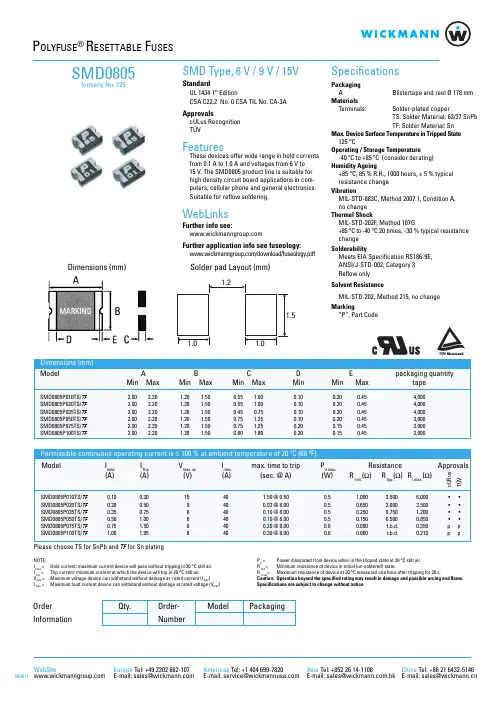
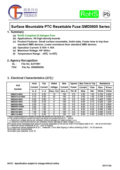
(a) RoHS Compliant & Halogen Free(b) Applications: All high-density boards(c) Product Features: Small surface mountable, Solid state, Faster time to trip thanstandard SMD devices, Lower resistance than standard SMD devices (d) Operation Current: 0.10A~1.10A (e) Maximum Voltage: 6V~24V DC(f) Temperature Range : -40℃ to 85℃2. Agency RecognitionUL : File No. E211981TÜV: File No. R500905563. Electrical Characteristics (23℃)H I T =Trip current-minimum current at which the device will always trip at 23℃ still air. V MAX =Maximum voltage device can withstand without damage at it rated current.(I MAX )I MAX = Maximum fault current device can withstand without damage at rated voltage (V MAX ).Pd=Typical power dissipated-type amount of power dissipated by the device when in the tripped state in 23℃ still air environment. R MIN =Minimum device resistance at 23℃ prior to tripping.R 1MAX =Maximum device resistance at 23℃ measured 1 hour after tripping or reflow soldering of 260℃ for 20 seconds. Termination pad characteristicsTermination pad materials: Pure Tin4.FSMD Product Dimensions (Millimeters)6. Typical Time-To-Trip at 23℃Tim e -t o -t r i p (S )7. Material SpecificationTerminal pad material: Pure TinSoldering characteristics: Meets EIA specification RS 186-9E, ANSI/J-std-002 Category 38. Part Numbering and Marking SystemPart Numbering System Part Marking SystemS M D □ □ □ - □ □ - 0805 F □Warning: electrical arcing and/or flame.-PPTC device are intended for occasional overcurrent protection. Application for repeated overcurrent condition and/or prolonged trip are not anticipated. 甲、 -Avoid contact of PPTC device with chemical solvent. Prolonged contact will damage the deviceperformance. A = SMD010-0805 / SMD010-24-0805 B = SMD020-0805 C = SMD035-0805 D = SMD050-0805 / SMD050-9-0805 E = SMD075-0805 F = SMD100-0805 G= SMD110-0805Current Rating Part Identification Logo Example Voltage Rating9. Pad Layouts 、Solder Reflow and Rework RecommendationsThe dimension in the table below provide the recommended pad layout for each SMD 0805 deviceNote 1: All temperatures refer to of the package,measured on the package body surface.Reflow Profile。

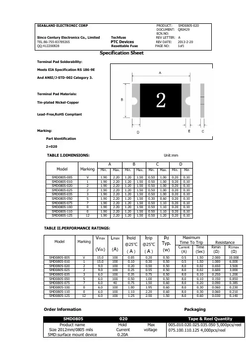
0805封装尺寸0402封装尺寸0603封装尺寸1206封装尺寸(转载)-jia...封装尺寸与功率关系:0201 1/20W0402 1/16W0603 1/10W0805 1/8W1206 1/4W封装尺寸与封装的对应关系0402=1.0mmx0.5mm0603=1.6mmx0.8mm0805=2.0mmx1.2mm1206=3.2mmx1.6mm1210=3.2mmx2.5mm1812=4.5mmx3.2mm2225=5.6mmx6.5mm贴片电阻电容常见封装有9种(电容指无级贴片),有英制和公制两种表示方式。
英制表示方法是采用4位数字表示的EIA(美国电子工业协会)代码,前两位表示电阻或电容长度,后两位表示宽度,以英寸为单位。
我们常说的0805封装就是指英制代码。
实际上公制很少用到,公制代码也由4位数字表示,其单位为毫米,与英制类似。
封装尺寸规格对应关系如下表:封装尺寸与功率有关通常如下:关于电容的封装除了上面的贴片封装外,对无极性电容,其封装模型还有RAD类型,例如“RAD-0.1”“RAD-0.2”等,后缀数字表示封装模型中两个焊盘间的距离,单位为英寸。
有极的电解电容的封装模型为RB类型,例如从“RB-.2/.4”到“RB-.5/.10”,其后缀的第一个数字表示封装模型中两个焊盘间的距离,第二个数字表示电容外形的尺寸,单位为也是英寸。
电阻:RES1,RES2,RES3,RES4;封装属性为axial系列无极性电容:cap;封装属性为RAD-0.1到rad-0.4电解电容:electroi;封装属性为rb.2/.4到rb.5/1.0电位器:pot1,pot2;封装属性为vr-1到vr-5二极管:封装属性为diode-0.4(小功率)diode-0.7(大功率)三极管:常见的封装属性为to-18(普通三极管)to-22(大功率三极管)to-3(大功率达林顿管)电源稳压块有78和79系列;78系列如7805,7812,7820等79系列有7905,7912,7920等常见的封装属性有to126h和to126v整流桥:BRIDGE1,BRIDGE2: 封装属性为D系列(D-44,D-37,D-46)电阻:AXIAL0.3-AXIAL0.7 其中0.4-0.7指电阻的长度,一般用AXIAL0.4瓷片电容:RAD0.1-RAD0.3。