
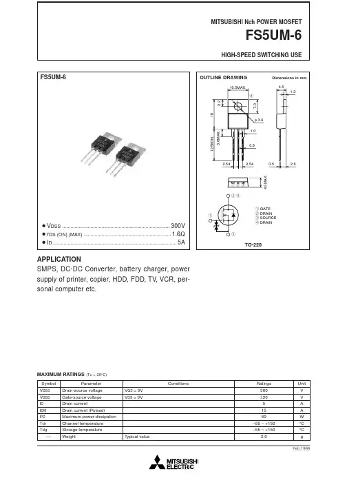
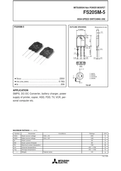
FS5UM-6中文资料
- 格式:pdf
- 大小:52.93 KB
- 文档页数:4

1.55 μm DFB-LD MODULE WITH SINGLEMODE FIBER PIGTAILModule type FU-650SDF-xW5M1 is a 1.55μm coaxialUncooled DFB-LD module with single-mode optical fiber.This module is suitable to a light source for use in2.5Gb/s digital optical communication systems.FEATURESlλ/4 shifted multiple quantum wells (MQW) DFBlaser diode modulel Emission wavelength is in 1.55μm bandl Built-in optical isolatorl Coaxial packagel With photodiode for optical output monitorAPPLICATIONHigh speed transmission systems (~2.5Gb/s)ABSOLUTE MAXIMUM RATINGS (Tc=25°C)UnitRatingParameter Symbol ConditionsOptical output power Pf CW 6 mWLaser diodeForward current If CW 150 mAReverse voltage Vrl - 2 VPhotodiodeReverse voltage Vrd - 20 VForward current Ifd - 2 mAOperating case temperature Tc - -5 ~ +85 °CStorage temperature Tstg - -40 ~ +85 °C1.55 μm DFB-LD MODULE WITH SINGLEMODE FIBER PIGTAIL ELECTRICAL/OPTICAL CHARACTERISTICS (Tc=-5~85°C, unless otherwise noted)LimitsParameter Symbol Test Conditions Min. Typ. Max.Unit CW, Tc=25°C - 10 20 Threshold current Ith CW 2 - 45mAOptical output power at threshold currentPth CW, Ibias=Ith - - 100 μWCW, Pf=2mW, Tc=25°C - 35 55 Operating current Iop CW, APC (Note 1), Tc=85°C - 60 110 mACW, Pf=2mW, Tc=25°C - 1.2 1.5 Operating voltage Vop CW, APC, Tc=85°C - 1.6 1.7VCW, Pf=2mW, Tc=25°C 14 25 40 Modulation Current (Iop-Ith) (Note 2) Imod CW, APC 10 - 65mADifferential impedance Rs - 3 6 10 ΩOptical output power from fiber endPf CW, nominal - 2 - mWLight-emission central wavelengthλcCW, APC 15301550 1570 nm Wavelength temperature coefficientλctCW, APC - 0.1 0.11 nm/°C Side mode suppression ratio Sr CW, APC 30 45 - dBRise and fall time (20~80%) tr, tf (Note 3) (Note 4) - 125 150 psecRelative intensity noise Nr CW, APC, f=1GHz - -145 -130 dB/HzTracking error (Note 5) Er CW, APC - 0.5 1.25 dBMonitor current Imon CW, Pf=2mW, Vrd=5V, Tc=25°C0.1 - 2 mAOptical isolation Iso - 20 - - dBDark current (PD) Id Vrd=5V - - 0.1 μACapacitance (PD) Ct Vrd=5V, f=1MHz - - 10 pFNote 1) “APC” represents operating LD by a constant monitor current for Pf=2mW at Tc=25°C.Note 2) Modulation current for LD driver shall be less than this “Imod” when the optical extinction ratio isset around 10dB.Note 3) 2.48832Gb/s NRZ, 223-1, Pf_ave=1mW, Ibias=Ith, optical return loss from the line should begreater than 24dB in order to ensure the specified performance.Note 4) Guaranteed only when the length of LD pins are shorter than 5mm.Note 5) Er=max|10×log(Pf / Pf@25°C)|FIBER PIGTAIL SPECIFICATIONSParameter Limits UnitType SM - Mode field diameter 10.5+/-1 μmCladding diameter 125+/-2 μmSecondary coating outer diameter 0.9+/-0.1 mmFiber length (Lfiber) 1000+/-100 mmConnector SC/PC -Optical return loss of connector 40 (min) dBDOCUMENTATION• Threshold current (Ith) at Tc=25, 85°C• Operating current (Iop) at Tc=25, 85°C• Operating voltage (Vop) at Tc=25°C• Light-emission central wavelength (λc) at Tc=25°C• Monitor current (Imon) at Tc=25°C• Optical output power from fiber end (Pf)ORDERING INFORMATIONFU-650SDF- x W5M1F : F-type pin assignment (see outline drawings)S : S-type(floating) pin assignment (see outline drawings)1.55μm DFB-LD MODULE WITH SINGLEMODE FIBER PIGTAILOUTLINE DIAGRAMNOTE. Tolerances unless noted +/-0.5FU-650SDF-FW5M1FU-650SDF-SW5M11.55 μm DFB-LD MODULE WITH SINGLEMODE FIBER PIGTAIL Safety Cautions for Use of Optoelectronic DevicesGeneral:Although the manufacturer is always striving to improve the reliability of its product, problems and errors may occur with semiconductor products. Therefore, the user's products are required to be designed with full safety regard to prevent any accidents that results in injury, death, fire or environmental damage even when semiconductor products happen to error. Especially it is recommended to take in consideration about redundancy, fire prevention, error prevention safeguards. And the following requirements must be strictly observed.Warning!1. Eye safety : Seminductor laser radiates laser light during operation. Laser light is very dangerous when shot directly into human eyes. Don't look at laser light directly, or through optics such as a lens. The laser light should be observed using the ITV camera, IR-viewer, or other appropriate instruments.2. Product handling : The product contains GaAs (gallium arsenide). It is safe for regular use, but harmful to the human body if made into powder or steam. Be sure to avoid dangerous process like smashing, burning, chemical etching. Never put this product in one's mouth or swallow it.3. Product disposal : This product must be disposed of as special industrial waste. It is necessary to separate it from general industrial waste and general garbage.Handling Cautions for Optoelectronic Devices1. General:(1) The products described in this specification are designed and manufactured for use in general communication systems or electronic devices, unless their applications or reliability are otherwise specified. Therefore, they are not designed or manufactured for installation in devices or systems that may affect human life or that are used in social infrastructure requiring high reliability.(2) When the customer is considering to use the products in special applications, such as transportation systems (automobiles, trains, vessels), medical equipments, aerospace, nuclear power control, and submarine repeaters or systems, please contact Mitsubishi Electric or an authorized distributor.2. Shipping Conditions:(1) During shipment, place the packing boxes in the correct direction, and fix them firmly to keep them immovable. Placing the boxes upside down, tilting, or applying abnormal pressure onto them may cause deformation in the electrode terminals, breaking of optical fiber, or other problems.(2) Never throw or drop the packing boxes. Hard impact on the boxes may cause break of the devices.(3) Take strict precautions to keep the devices dry when shipping under rain or snow.3. Storage Conditions:When storing the products, it is recommended to store them following the conditions described below without opening the packing. Not taking enough care in storing may result in defects in electrical characteristics, soldering quality, visual appearance, and so on. The main points are described below (if special storage conditions are given to the product in the specification sheet, they have priority over the following general cautions):(1) Appropriate temperature and humidity conditions, i.e., temperature range between 5~30°C, and humidity between 40~60 percent RH, should be maintained in storage locations. Controlling the temperature and humidity within this range is particularly important in case of long-term storage for six months or more.(2) The atmosphere should be particularly free from toxic gases and dust.(3) Do not apply any load on the product.(4) Do not cut or bend the leads of the devices which are to be stored. This is to prevent corrosion in the cut or bent part of the lead causing soldering problems in the customer’s assembling process.(5) Sudden change in temperature may cause condensation in the product or packing, therefore, such locations should be avoided for storing. Temperature in storage locations should be stable.(6) When storing ceramic package products for extended periods of time, the leads may turn reddish due to reaction with sulfur in the atmosphere.(7) Storage conditions for bare chip and unsealed products shall be stated separately because bare chip and unsealed products require stricter controls than package sealed products.4. Design Conditions and Environment under Use:(1) Avoid use in locations where water or organic solvents adhere directly to the product, or where there is any possibility of the generation of corrosive gas, explosive gas, dust, salinity, or other troublesome conditions. Such environments will not only significantly lower the reliability, but also may lead to serious accidents.(2) Operation in excess of the absolute maximum ratings can cause permanent damage to the device. The customers are requested to design not to exceed those ratings even for a short time.5. ESD Safety Cautions:The optoelectronic devices are sensitive to static electricity (ESD, electro-static discharge). The product can be broken by ESD. When handling this product, please observe the following countermeasures:<Countermeasures against Static Electricity and Surge>To prevent break of devices by static electricity or surge, please adopt the following countermeasures in the assembly line:(1) Ground all equipments, machinery jigs, and tools in the process line with earth wires installed in them. Take particular care with hot plates, solder irons and other items for which the commercial power supplies are prone to leakage.(2) Workers should always use earth bands. Use of antistatic clothing, electric conductive shoes, and other safety equipment while at work is highly recommended.(3) Use conductive materials for this product’s container, etc.(4) It is recommended that grounding mats be placed on the surfaces of assembly line workbench and the surrounding floor in work area, etc.(5) When mounting this product in parts or materials which can be electrically charged (printed wiring boards, plastic products, etc.), pay close attention to the static electricity in those parts. ESD may damage the product.(6) Humidity in working environment should be controlled to be 40 percent RH or higher.These countermeasures are most general, and there is a need to carefully confirm the line before starting mass production using this product (in the trial production, etc.). It is extremely important to prevent surge, eliminate it rapidly, and prevent it from spreading.。

UNISONIC TECHNOLOGIES CO., LTD50N06MOSFET50 Amps, 60 VoltsN-CHANNEL POWER MOSFETDESCRIPTIONThe UTC 50N06 is three-terminal silicon device with current conduction capability of about 50A, fast switching speed. Low on-state resistance, breakdown voltage rating of 60V, and max threshold voltages of 4 volt.It is mainly suitable electronic ballast, and low power switching mode power appliances.FEATURES* R DS(ON) = 23m Ω@V GS = 10 V* Ultra low gate charge ( typical 30 nC )* Low reverse transfer Capacitance ( C RSS = typical 80 pF ) * Fast switching capability* 100% avalanche energy specified * Improved dv/dt capabilitySYMBOL1.GateTO-22011TO-220F*Pb-free plating product number: 50N06LORDERING INFORMATIONOrder Number Pin AssignmentNormalLead Free Plating Package 1 2 3 Packing50N06-TA3-T 50N06L-x-TA3-T TO-220 G D S Tube 50N06-TF3-T 50N06L-x-TF3-T TO-220F G D S TubeABSOLUTE MAXIMUM RATINGSPARAMETER SYMBOL RATINGS UNITDrain-Source Voltage V DSS 60 V Gate to Source Voltage V GSS ±20 VT C = 25 50 AContinuous Drain Current T C = 100 I D35 ADrain Current Pulsed (Note 1) I DM 200 A Single Pulsed Avalanche Energy (Note 2) E AS 480 mJ Repetitive Avalanche Energy (Note 1) E AR 13 mJ Peak Diode Recovery dv/dt (Note 3) dv/dt 7 V/nsTotal Power Dissipation (T C = 25 ) 130 WDerating Factor above 25P D0.9 W/ Operation Junction Temperature T J -55 ~ +150 Storage Temperature T STG -55 ~ +150 Note: Absolute maximum ratings are those values beyond which the device could be permanently damaged.Absolute maximum ratings are stress ratings only and functional device operation is not implied.THERMAL DATAPARAMETER SYMBOL MIN TYP MAX UNITThermal Resistance, Junction-to-Case θJC 1.15 °C/W Thermal Resistance, Case-to-Sink θCS 0.5 °C/W Thermal Resistance, Junction-to-Ambient θJA 62.5 °C/WELECTRICAL CHARACTERISTICS T C = 25 unless otherwise specifiedPARAMETER SYMBOL TEST CONDITIONS MIN TYP MAX UNIT Off CharacteristicsDrain-Source Breakdown Voltage BV DSS V GS = 0 V, I D = 250 µA 60 V Breakdown Voltage Temperature Coefficient BV DSS /△T J I D = 250 µA,Referenced to 250.07 V/V DS = 60 V, V GS = 0 V µADrain-Source Leakage Current I DSSV DS = 48 V, T C = 1251 µA Gate-Source Leakage Current V GS = 20V, V DS = 0 V 100 nAGate-Source Leakage Reverse I GSSV GS = -20V, V DS = 0 V -100 nA On Characteristics Gate Threshold Voltage V GS(TH) V DS = V GS , I D = 250 µA 2.0 4.0 V Static Drain-Source On-StateResistanceR DS(ON) V GS = 10 V, I D = 25 A 18 23 m ΩDynamic Characteristics Input Capacitance C ISS 900 1220 pFOutput Capacitance C OSS 430 550 pFReverse Transfer Capacitance C RSSV GS = 0 V, V DS = 25 Vf = 1MHz80 100 pF Dynamic Characteristics Turn-On Delay Time t D(ON) 40 60 nsRise Time t R 100 200 ns Turn-Off Delay Time t D(OFF) 90 180 nsFall Time t F V DD = 30V, I D =25 A, R G = 50Ω (Note 4, 5) 80 160 ns Total Gate Charge Q G 30 40 nCGate-Source Charge Q GS 9.6 nCGate-Drain Charge (Miller Charge) Q GD V DS = 48V, V GS = 10 VI D = 50A, (Note 4, 5)10 nC2. L=5.6mH, I AS=50A, V DD=25V, R G=0Ω, Starting T J=253. I SD≤50A, di/dt≤300A/µs, V DD≤BV DSS, Starting T J=254. Pulse Test: Pulse Width≤300µs,Duty Cycle≤2%5. Essentially independent of operating temperature.TEST CIRCUITS AND WAVEFORMSV DDV GS (Driver)I SD (D.U.T.)Body DiodeForward Voltage DropV DS(D.U.T.)Fig. 1A Peak Diode Recovery dv/dt Test CircuitFig. 1B Peak Diode Recovery dv/dt WaveformsTEST CIRCUITS AND WAVEFORMS (Cont.)R LDDV DS90%10%V GStFig. 2A Switching Test Circuit Fig. 2B Switching WaveformsFig. 3A Gate Charge Test CircuitFig. 3B Gate Charge Waveform10VLV DDI ASFig. 4A Unclamped Inductive Switching Test Circuit Fig. 4B Unclamped Inductive Switching WaveformsTYPICAL CHARACTERISTICS101010101010Drain -Source Voltage , V DS (V)D r a i n C u r r e n t , I D (A )On-State Characteristics101010Gate-Source Voltage , V GS (V)D r a i n C u r r e n t , I D (A )Transfer Characteristics0D r a i n -S o u r c e O n -R e s i s t a n c e , R D S (O N ) (m Ω)Drain Current , I D (A)4080200100140On-Resistance Variation vs . Drain Current102101000.2Source-Drain Voltage , V SD (V)R e v e r s e D r a i n C u r r e n t , I S D (A )On State Current vs. Allowable CaseTemperature1.60.40.60.8 1.0 1.2 1.420601201601805Drain -Source Voltage, V DC (V)C a p a c i t a n c e (p F )Capacitance Characteristics1020G a t e -t o -S o u r c e V o l t a g e , V G S (V )Total Gate Charge , Q G (nC)81012Gate Charge Characteristics64015253035TYPICAL CHARACTERISTICS(Cont.)-100D r a i n -S o u r c e B r e a k d o w n V o l t a g e , B V D S S (N o r m a l i z e d )Junction Temperature , T J (℃)-5050200100150Breakdown Voltage Variation vs . Junction, -5050100150On-Resistance Variation vs . 0Junction Temperature , T J (℃)101010Drain-Source Voltage , V DS (V)D r a i n C u r r e n t , I D ,(A )Maximum Safe Operating1010D r a i n C u r r e n t , I D (A )Case Temperature, T C (℃)7510050Maximum Drain Current vs . Case Temperature 01255025102030401010101010Square Wave Pulse Duration , t 1 (sec)T h e r m a l R e s p o n s e , Z θJ C (t )1010101010101010101Transient Thermal。
