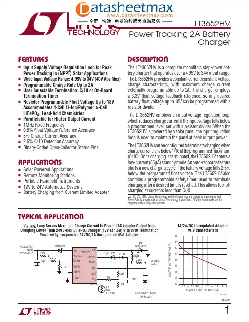
TMFEATURESAPPLICATIONSDESCRIPTIONTHD+N–TotalHarmonicDistortion+Noise–%1070G0120.010.12010.110P O – Output Power – W1TAS5186ASLES156–OCTOBER2005 6-Channel,210-W,Digital-Amplifier Power StageThe TAS5186A requires only simple passivedemodulation filters on its outputs to deliver •Total Output Power@10%THD+Nhigh-quality,high-efficiency audio amplification.The –5×30W@6Ω+1×60W@3Ωdevice efficiency of the TAS5186A is greater than90%when driving6-Ωsatellites and a3-Ωsubwoofer •105-dB SNR(A-Weighted)speaker.•0.07%THD+N@1WThe TAS5186A has an innovative protection system •Power Stage Efficiency>90%Intointegrated on-chip,safeguarding the device against a Recommended Loads(SE)wide range of fault conditions that could damage the •Integrated Self-Protection Circuits system.These safeguards are short-circuit protection,–Undervoltage overload protection,undervoltage protection,andovertemperature protection.The TAS5186A has a –Overtemperaturenew proprietary current-limiting circuit that reduces –Overloadthe possibility of device shutdown during high-level –Short Circuit music transients.A new programmable overcurrentdetector allows the use of lower-cost inductors in the •Integrated Active-Bias Control to Avoid DCdemodulation output filter.Pop•Thermally Enhanced44-Pin HTSSOP Package TOTAL HARMONIC DISTORTION+NOISEvs•EMI-Compliant When Used WithOUTPUT POWER Recommended System Design•DVD Receiver•Home Theater in a BoxThe TAS5186A is a high-performance,six-channel,digital-amplifier power stage with an improvedprotection system.The TAS5186A is capable ofdriving a6-Ω,s ingleended load up to30W per eachfront/satellite channel and a3-Ω,single-endedsubwoofer greater than60W at10%THD+Nperformance.A low-cost,high-fidelity audio system can be builtusing a TI chipset comprising a modulator(e.g.,TAS5086)and the TAS5186A.This device does notrequire power-up sequencing because of the internalpower-on reset.Please be aware that an important notice concerning availability,standard warranty,and use in critical applications of TexasInstruments semiconductor products and disclaimers thereto appears at the end of this data sheet.PowerPAD is a trademark of Texas Instruments.PRODUCTION DATA information is current as of publication date.Copyright©2005,Texas Instruments Incorporated Products conform to specifications per the terms of the TexasInstruments standard warranty.Production processing does notnecessarily include testing of all parameters.DDV PACKAGE (TOP VIEW)P0016-03TAS5186ASLES156–OCTOBER 2005These devices have limited built-in ESD protection.The leads should be shorted together or the device placed in conductive foam during storage or handling to prevent electrostatic damage to the MOS gates.The TAS5186A is available in a thermally enhanced 44-pin HTSSOP PowerPAD™package.The heat slug is located on the top side of the device for convenient thermal coupling to a heatsink.2TAS5186ASLES156–OCTOBER 2005GENERAL INFORMATION (continued)TERMINAL FUNCTIONSTERMINAL TYPE (1)DESCRIPTIONNAME NO.AGND 12P Analog groundBST_A 23P HS bootstrap supply (BST),capacitor to OUT_A required BST_B 29P HS bootstrap supply (BST),external capacitor to OUT_B required BST_BIAS 21P BIAS bootstrap supply,external capacitor to OUT_BIAS required BST_C 30P HS bootstrap supply (BST),external capacitor to OUT_C required BST_D 37P HS bootstrap supply (BST),external capacitor to OUT_D required BST_E 38P HS bootstrap supply (BST),external capacitor to OUT_E required BST_F 44P HS bootstrap supply (BST),external capacitor to OUT_F required GND 11P Chip groundGVDD_ABC 20P Gate drive voltage supply GVDD_DEF 3P Gate drive voltage supply M110I Mode selection pin M29I Mode selection pin M38I Mode selection pinOC_ADJ 14O Overcurrent threshold programming pin,resistor to ground required OTW 16O Overtemperature warning open-drain output signal,active-low OUT_A 25O Output,half-bridge A,satellite OUT_B 27O Output,half-bridge B,satellite OUT_BIAS 22O BIAS half-bridge output pin OUT_C 32O Output,half-bridge C,subwoofer OUT_D 35O Output,half-bridge D,satellite OUT_E 40O Output,half-bridge E,satellite OUT_F42OOutput,half-bridge F,satellite1,26,PGND 33,P Power ground34,41PVDD_A 24P Power-supply input for half-bridge A PVDD_B 28P Power-supply input for half-bridge B PVDD_C 31P Power-supply input for half-bridge C PVDD_D 36P Power-supply input for half-bridge D PVDD_E 39P Power-supply input for half-bridge E PVDD_F 43P Power-supply input for half-bridge F PWM_A 19I PWM input signal for half-bridge A PWM_B 18I PWM input signal for half-bridge B PWM_C 17I PWM input signal for half-bridge C PWM_D 6I PWM input signal for half-bridge D PWM_E 5I PWM input signal for half-bridge E PWM_F 2I PWM input signal for half-bridge F RESET 7I Reset signal (active-low logic)SD 15O Shutdown open-drain output signal,active-low VDD 4P Power supply for digital voltage regulator VREG 13ODigital regulator supply filter pin,output(1)I =input;O =output;P =power3PACKAGE HEAT DISSIPATION RATINGS (1)ABSOLUTE MAXIMUM RATINGSTAS5186ASLES156–OCTOBER 2005Table 1.MODE Selection PinsMODE PINS (1)MODEM2M3NAMEDESCRIPTION00 2.1mode Channels A,B,and C enabled;channels D,E,and F disabled01 5.1mode All channels enabled10/1Reserved(1)M1must always be connected to GND.0indicates a pin connected to GND;1indicates a pin connected to VREG.PARAMETERTAS5186ADDVR θJC (°C/W)—1satellite (sat.)FET only 10.3R θJC (°C/W)—1subwoofer (sub.)FET only5.2R θJC (°C/W)—1sat.half-bridge 5.2R θJC (°C/W)—1sub.half-bridge 2.6R θJC (°C/W)—5sat.half-bridges +1sub.1.74Typical pad area (2)34.9mm 2(1)JC is junction-to-case,CH is case-to-heatsink.(2)R θCH is an important consideration.Assume a 2-mil thickness of typical thermal grease between the pad area and the heatsink.The R θCH with this condition is typically 2°C/W for this package.over operating free-air temperature range (unless otherwise noted)(1)TAS5186AVDD to AGND –0.3V to 13.2V GVDD_X to AGND –0.3V to 13.2V PVDD_X to PGND_X (2)–0.3V to 50V OUT_X to PGND_X (2)–0.3V to 50V BST_X to PGND_X (2)–0.3V to 63.2V VREG to AGND –0.3V to 4.2V PGND to GND –0.3V to 0.3V PGND to AGND –0.3V to 0.3V GND to AGND–0.3V to 0.3V PWM_X,OC_ADJ,M1,M2,M3to AGND –0.3V to 4.2V RESET,SD,OTW to AGND–0.3V to 7V Maximum operating junction temperature range (T J )0to 125°C Storage temperature–40°C to 125°CLead temperature –1,6mm (1/16inch)from case for 10seconds 260°C Minimum PWM pulse duration,low 30ns(1)Stresses beyond those listed under absolute maximum ratings may cause permanent damage to the device.These are stress ratings only,and functional operation of the device at these or any other conditions beyond those indicated under recommended operating conditions is not implied.Exposure to absolute-maximum-rated conditions for extended periods may affect device reliability.(2)These voltages represent the dc voltage +peak ac waveform measured at the terminal of the device in all conditions.4M1M2RESETSD OTWAGND OC_ADJVREG VDDGVDD_DEF M3GNDPWM_FOUT_F PGND PVDD_FBST_FPWM_EOUT_E PGND PVDD_E BST_EPWM_DOUT_D PGND PVDD_D BST_DPWM_COUT_C PGND PVDD_C BST_CPWM_BOUT_B PGND PVDD_B BST_BPWM_AOUT_APVDD_A BST_AOUT_BIASBST_BIASB0034-03GVDD_ABC TAS5186ASLES156–OCTOBER 2005TYPICAL SYSTEM DIAGRAMA schematic diagram for a typical system is appended at the end of the data sheet.FUNCTIONAL BLOCK DIAGRAM5RECOMMENDED OPERATING CONDITIONSAUDIO SPECIFICATIONTAS5186ASLES156–OCTOBER 2005MINTYPMAX UNIT PVDD_X Half-bridge supply,SEDC supply voltage at pin(s)040V GVDD Gate drive and guard ring supply voltage DC voltage at pin(s)10.81213.2V VDD Digital regulator supply DC supply voltage at pin 10.81213.2V Any value of R PU,EXT within VPU Pullup voltage supply35 5.5V recommended rangeResistive load impedance,satellite Recommended demodulation filter R L,SAT 46Ωchannels (1)Resistive load impedance,subwoofer Recommended demodulation filter R L,SUB 2.253ΩchannelMinimum output inductance under L output Demodulation filter inductance 522µH short-circuit conditionC output,sat Demodulation filter capacitance 1µF C output,sub Demodulation filter capacitance 1µF F PWM PWM frame rate192384432kHz(1)Load impedance outside range listed might cause shutdown due to OLP,OTE,or NLP.PVDD_X =40V,GVDD =12V,audio frequency =1kHz,AES17measurement filter,F PWM =384kHz,case temperature =75°C.Audio performance is recorded as a chipset,using TAS5086PWM processor with an effective modulation index limit of 97%.All performance is in accordance with the foregoing specifications and recommended operating conditions unless otherwise specified.PARAMETERCONDITIONSMINTYP MAXUNITR L =6Ω,10%THD,clipped input signal30R L =8Ω,10%THD,clipped input signal 25P O,satPower output per satellite channelWR L =6Ω,0dBFS,unclipped input signal 25R L =8Ω,0dBFS,unclipped input signal 20R L =3Ω,10%THD,clipped input signal60R L =4Ω,10%THD,clipped input signal 52P O,subPower output,subwooferW R L =3Ω,0dBFS,unclipped input signal 50R L =4Ω,0dBFS,unclipped input signal40R L =6Ω,P O =25W 0.3%Total harmonic distortion +noise,satelliteR L =6Ω,1W 0.07%THD +NR L =3Ω,P O =50W 0.5%Total harmonic distortion +noise,subwooferR L =3Ω,1W 0.05%Output integrated noise,satellite A-weighted 55V n µV Output integrated noise,subwoofer A-weighted 60SNR System signal-to-noise ratio A-weighted105dB Dynamic range (1)A-weighted,–60dBFS input signal,105DNRdB measured with TAS5086PWM processor P O =0W,all channels running 5.1mode (2).22-µH Kwang-Sung inductors (see 4.5W Power dissipation due to idle losses schematic for information)P idle(IPVDDX)P O =0W,2.1mode.22-µH Kwang-Sung 2.2W inductors (see schematic for information)(1)SNR is calculated relative to 0-dBFS input level.(2)Actual system idle losses are affected by core losses of output inductors.6ELECTRICAL CHARACTERISTICSTAS5186ASLES156–OCTOBER 2005F PWM =384kHz,GVDD =12V,VDD =12V,T C (case temperature)=75°C,unless otherwise noted.All performance is in accordance with recommended operating conditions,unless otherwise specified.SYMBOL PARAMETERCONDITIONSMIN TYP MAX UNIT INTERNAL VOLTAGE REGULATOR ANDCURRENT CONSUMPTIONVREG Voltage regulator,only used as reference node VDD =12V33.3 3.6V Operating,50%duty cycle 720IVDD VDD supply currentmA Idle,reset mode 61650%duty cycle 522IGVDD_XGate supply current per half-bridgemAIdle,reset mode1350%duty cycle,without output filter or load,5.1110mode.22-µH Kwang-Sung inductorsIPVDD_X Half-bridge idle currentmA50%duty cycle,without output filter or load,2.160mode.22-µH Kwang-Sung inductors OUTPUT STAGE MOSFETs R DSon ,LS Sat Drain-to-source resistance,low side,satellite T J =25°C,includes metallization resistance 210m ΩR DSon ,HS Sat Drain-to-source resistance,high side,satellite T J =25°C,includes metallization resistance 210m ΩR Dson ,LS Sub Drain-to-source resistance,low side,subwoofer T J =25°C,includes metallization resistance 110m ΩR Dson ,HS Sub Drain-to-source resistance,high side,subwooferT J =25°C,includes metallization resistance110m ΩI/O PROTECTION V UVP,G Undervoltage protection limit GVDD_X 10V V UVP,hyst (1)Undervoltage protection hysteresis 250mV OTW (1)Overtemperature warning125°C Temperature drop needed below OTW temp.for OTW hyst (1)25°C OTW to be inactive after the OTW event OTE (1)Overtemperature error155°C Temperature drop needed below OTE temp.for SD OTE HYST (1)25°C to be released after the OTE event OLCP Overload protection counter 1.25ms Overcurrent limit protection,satellite Rocp =18k Ω 4.5A I OC Overcurrent limit protection,subwoofer Rocp =18k Ω8A I OCT Overcurrent response time 210ns Rocp OC programming resistor range Resistor tolerance =5%18k ΩSTATIC DIGITAL SPECIFICATIONV IH High-level input voltage 2PWM_X,M1,M2,M3,RESET V V IL Low-level input voltage 0.8I LEAKInput leakage currentStatic condition–8080µAOTW/SHUTDOWN (SD)Internal pullup resistor to DREG (3.3V)for SD and R INT_PU 26k ΩOTWInternal pullup resistor only3 3.33.6V OH High-level output voltage External pullup:4.7-k Ωresistor to 5V 4.55V V OL Low-level output voltage I O =4mA 0.20.4FANOUTDevice fanout OTW,SDNo external pullup30Devices (1)Specified by design.7TYPICAL CHARACTERISTICS,5.1MODET H D +N – T o t a l H a r m o n i c D i s t o r t i o n + N o i s e – %1040G0010.010.12010.110P O – Output Power – W1T H D +N – T o t a l H a r m o n i c D i s t o r t i o n + N o i s e – %1070G0020.010.12010.110P O – Output Power – W1PVDD – Supply Voltage – V 024681012141618202224262830323436P O – O u t p u t P o w e r – WG003PVDD – Supply Voltage – V510152025303540455055606570G004P O – O u t p u t P o w e r – WTAS5186ASLES156–OCTOBER 2005TOTAL HARMONIC DISTORTION +NOISETOTAL HARMONIC DISTORTION +NOISEvsvsOUTPUT POWEROUTPUT POWERFigure 1.Figure 2.OUTPUT POWEROUTPUT POWERvsvsSUPPLY VOLTAGESUPPLY VOLTAGEFigure 3.Figure 4.8PVDD – Supply Voltage – V 0246810121416182022242628G005P O – O u t p u t P o w e r – WPVDD – Supply Voltage – V0510152025303540455055G006P O – O u t p u t P o w e r – W20406080100120140160180200220240S y s t e m E f f i c i e n c y – %G007P O – Total Output Power – W051015202530354020406080100120140160180200220240S y s t e m P o w e r L o s s – WG008P O – Total Output Power – WTAS5186ASLES156–OCTOBER 2005TYPICAL CHARACTERISTICS,5.1MODE (continued)OUTPUT POWEROUTPUT POWERvsvsSUPPLY VOLTAGESUPPLY VOLTAGEFigure 5.Figure 6.SYSTEM EFFICIENCYSYSTEM POWER LOSSvsvsTOTAL OUTPUT POWERTOTAL OUTPUT POWERFigure 7.Figure 8.9T C – Case Temperature – °C 0510********35402030405060708090100110G009P O – O u t p u t P o w e r – WT C – Case Temperature – °C010203040506070802030405060708090100110G010P O – O u t p u t P o w e r – Wf – Frequency – kHz−150−140−130−120−110−100−90−80−70−60−50−40−30−20−1000246810121416182022A m p l i t u d e – d BG011TAS5186ASLES156–OCTOBER 2005TYPICAL CHARACTERISTICS,5.1MODE (continued)OUTPUT POWEROUTPUT POWERvsvsCASE TEMPERATURECASE TEMPERATUREFigure 9.Figure 10.AMPLITUDEvsFREQUENCYFigure 11.10 THEORY OF OPERATIONPOWER SUPPLIESSYSTEM POWER-UP/DOWN SEQUENCE Powering Down Error Reporting TAS5186ASLES156–OCTOBER 2005reliability,it is important that each PVDD_X pin is decoupled with a 100-nF ceramic capacitor placed as close as possible to each supply pin on the same To facilitate system design,the TAS5186A needsside of the PCB as the TAS5186A.It is only a 12-V supply in addition to a typical 39-Vrecommended to follow the PCB layout of the power-stage supply.An internal voltage regulatorTAS5186A reference design.For additional provides suitable voltage levels for the digital andinformation on the recommended power supply and low-voltage analog circuitry.Additionally,all circuitryrequired components,see the application diagrams requiring a floating voltage supply,e.g.,the high-sidegiven in this data sheet.The 12-V supply should be gate drive,is accommodated by built-in bootstrappowered from a low-noise,low-output-impedance circuitry requiring only a few external capacitors.voltage regulator.Likewise,the 39-V power-stage supply is assumed to have low output impedance and In order to provide outstanding electrical and acousticlow noise.The power-supply sequence is not critical characteristics,the PWM signal path including gatedue to the internal power-on-reset circuit.Moreover,drive and output stage is designed as identical,the TAS5186A is fully protected against erroneous independent half-bridges.For this reason,eachpower-stage turnon due to parasitic gate charging.half-bridge has separate bootstrap pins (BST_X)andThus,voltage-supply ramp rates (dv/dt)are typically power-stage supply pins (PVDD_X).Furthermore,annoncritical.additional pin (VDD)is provided as power supply forall common circuits.Although supplied from the same12-V source,it is highly recommended to separateGVDD_X and VDD on the printed-circuit board (PCB)The TAS5186A does not require a power-up by RC filters (see application diagram for details).sequence.The outputs of the H-bridge remain in a These RC filters provide the recommendedhigh-impedance state until the gate-drive supply high-frequency isolation.Special attention should bevoltage (GVDD_X)and VDD voltage are above the paid to placing all decoupling capacitors as close toundervoltage protection (UVP)voltage threshold (see their associated pins as possible.In general,the Electrical Characteristics section of this data inductance between the power-supply pins andsheet).Although not specifically required,it is decoupling capacitors must be avoided.(Seerecommended to hold RESET in a low state while reference board documentation for additionalpowering up the rmation.)When the TAS5186A is being used with TI PWM For a properly functioning bootstrap circuit,a smallmodulators such as the TAS5086,no special ceramic capacitor must be connected from eachattention to the state of RESET is required,provided bootstrap pin (BST_X)to the power-stage output pinthat the chipset is configured as recommended.(OUT_X).When the power-stage output is low,thebootstrap capacitor is charged through an internaldiode connected between the gate-drivepower-supply pin (GVDD_X)and the bootstrap pin.The TAS5186A does not require a power-down When the power-stage output voltage is high,thesequence.The device remains fully operational as bootstrap capacitor voltage is shifted above thelong as the gate-drive supply (GVDD_X)voltage and output voltage potential and thus provides a suitableVDD voltage are above the undervoltage protection voltage supply for the high-side gate driver.In an(UVP)threshold level (see the Electrical application with PWM switching frequencies in theCharacteristics section of this data sheet).Although range 352kHz to 384kHz,it is recommended to usenot specifically required,it is a good practice to hold 33-nF ceramic capacitors,size 0603or 0805,for theRESET low during power down,thus preventing bootstrap capacitor.These 33-nF capacitors ensureaudible artifacts including pops and clicks sufficient energy storage,even during minimal PWMWhen the TAS5186A is being used with TI PWM duty cycles,to keep the high-side power stage FETmodulators such as the TAS5086,no special (LDMOS)fully started during all of the remaining partattention to the state of RESET is required,provided of the PWM cycle.In an application running at athat the chipset is configured as recommended.reduced switching frequency,generally 250kHz to192kHz,the bootstrap capacitor might need to beincreased in value.Special attention should be paidto the power-stage power supply;this includesThe SD and OTW pins are both active-low,component selection,PCB placement and routing.Asopen-drain outputs.Their function is for indicated,each half-bridge has independentprotection-mode signaling to a PWM controller or power-stage supply pins (PVDD_X).For optimalother system-control device.electrical performance,EMI compliance,and systemDevice Protection SystemOVERCURRENT (OC)PROTECTION WITH TAS5186ASLES156–OCTOBER 2005Any fault resulting in device shutdown is signaled bytwo protection systems.The first protection system the SD pin going low.Likewise,OTW goes low whencontrols the power stage in order to prevent the the device junction temperature exceeds 125°C (seeoutput current from further increasing.i.e.,it performs the following table).a current-limiting function rather than prematurely shutting down during combinations of high-level music transients and extreme speaker SDOTW DESCRIPTION load-impedance drops.If the high-current situation persists,i.e.,the power stage is being overloaded,a 00Overtemperature (OTE)or overload (OLP)or undervoltage (UVP)second protection system triggers a latching shutdown,resulting in the power stage being set in 01Overload (OLP)or undervoltage (UVP)the high-impedance (Hi-Z)state.10Overtemperature warning.Junction temperature higher than 125°C,typical For added flexibility,the OC threshold is 11Normal operation.Junction temperature lower thanprogrammable within a limited range using a single 125°C,typical external resistor connected between the OC_ADJ pinand AGND.It should be noted that asserting RESET low forces OC-Adjust Resistor ValuesMaximum Peak Current Before the SD and OTW signals high independently of faults (k Ω)OC Occurs (A)being present.It is recommended to monitor the 18 4.5(sat.),8(sub.)OTW signal using the system microcontroller and torespond to an overtemperature warning signal by,It should be noted that a properly functioning e.g.,turning down the volume to prevent furtherovercurrent detector assumes the presence of a heating of the device that would result in deviceproperly designed demodulation filter at the shutdown (OTE).To reduce external componentpower-stage output.Short-circuit protection is not count,an internal pullup resistor to 3.3V is providedprovided directly at the output pins of the power stage on both the SD and OTW outputs.Level compliancebut only on the speaker terminals (after the for 5-V logic can be obtained by adding externaldemodulation filter).It is required to follow certain pullup resistors to 5V (see the Electricalguidelines when selecting the OC threshold and an Characteristics section of this data sheet for furtherappropriate demodulation inductor.specifications).•For the lowest-cost bill of materials in terms of component selection,the OC threshold current should be limited,considering the power output The TAS5186A contains advanced protection circuitryrequirement and minimum load impedance.carefully designed to facilitate system integration andHigher-impedance loads require a lower OC ease of use,as well as safeguarding the device fromthreshold.permanent failure due to a wide range of fault•The demodulation filter inductor must retain at conditions such as short circuit,overload,andleast 5µH of inductance at twice the OC undervoltage.The TAS5186A responds to a fault bythreshold setting.immediately setting the power stage in ahigh-impedance state (Hi-Z)and asserting the SD pinMost inductors have decreasing inductance with low.In situations other than overload,the deviceincreasing temperature and increasing current automatically recovers when the fault condition has(saturation).To some degree,an increase in been removed,e.g.,the supply voltage has increasedtemperature naturally occurs when operating at high or the temperature has dropped.For highest possibleoutput currents,due to inductor core losses and the reliability,recovering from an overload fault requiresdc resistance of the inductor copper winding.A external reset of the device no sooner than 1secondthorough analysis of inductor saturation and thermal after the shutdown (see the Device Reset section ofproperties is strongly recommended.this data sheet).Setting the OC threshold too low might cause issuessuch as lack of output power and/or unexpectedshutdowns due to sensitive overload detection.CURRENT LIMITING AND OVERLOAD DETECTION In general,it is recommended to follow closely theexternal component selection and PCB layout asThe device has independent,fast-reacting currentgiven in the application section.detectors with programmable trip threshold (OCthreshold)on all high-side and low-side power-stageFETs.See the following table for OC-adjust resistorvalues.The detector outputs are closely monitored by Overtemperature ProtectionUNDERVOLTAGE PROTECTION (UVP)AND DEVICE RESET ACTIVE-BIAS CONTROL (ABC)TAS5186ASLES156–OCTOBER 2005element in the audio path,i.e.,split-cap capacitors or series capacitor,to the desired potential before The TAS5186A has a two-levelswitching is started on the PWM outputs.(For temperature-protection system that asserts anrecommended configuration,see the typical active-low warning signal (OTW)when the deviceapplication schematic included in this data sheet).junction temperature exceeds 125°C (typical),and Ifthe device junction temperature exceeds 155°CThe start-up sequence can be controlled through (typical),the device is put into thermal shutdown,sequencing the M3and RESET pins according to resulting in all half-bridge outputs being set in theTable 2and Table 3.high-impedance state (Hi-Z)and SD being assertedlow.Table 2.5.1Mode—All Output Channels ActiveM3RESET OUT_BIAS OUT_A,OUT_D,COMMENT _B,_C _E,_FPOWER-ON RESET (POR)00Hi-Z Hi-Z Hi-Z All outputsdisabled,The UVP and POR circuits of the TAS5186A fully nothing isprotect the device in any power-up/down and switching.brownout situation.While powering up,the POR 10Active Hi-Z Hi-Z OUT_BIAScircuit resets the overload circuit (OLP)and ensures enabled,allthat all circuits are fully operational when the other outputsdisabledGVDD_X and VDD supply voltages reach 10V (typical).Although GVDD_X and VDD are 11Hi-Z Active Active OUT_BIASdisabled,allindependently monitored,a supply voltage drop other outputsbelow the UVP threshold on any VDD or GVDD_Xswitching pin results in all half-bridge outputs immediately beingset in the high-impedance (Hi-Z)state and SD beingTable 3.2.1Mode—Only Output Channels A,B,asserted low.The device automatically resumesand C Active operation when all supply voltages have increasedabove the UVP threshold.M3RESET OUT_BIAS OUT_A,OUT_D,COMMENT _B,_C _E,_F00Hi-Z Hi-Z Hi-Z All outputsdisabled,When RESET is asserted low,the output FETs in all nothing ishalf-bridges are forced into a high-impedance (Hi-Z)switching.state.10Active Hi-Z Hi-Z OUT_BIASenabled,allAsserting the RESET input low removes any fault other outputsinformation to be signaled on the SD output,i.e.,SD disabledis forced high.01Hi-Z Active Hi-ZOUT_BIASdisabled,allA rising-edge transition on the RESET input allows other outputsthe device to resume operation after an overloadswitching fault.When the TAS5186A is used with the TAS5086PWM modulator,no special attention to start-up sequencing is required,provided that the chipset is configured as Audible pop noises are often associated withrecommended.single-rail,single-ended power stages at power-up orat the start of switching.This commonly knownproblem has been virtually eliminated byincorporating a proprietary active-bias control circuitryas part of the TAS5186A feature set.By the use ofonly a few passive external components (typicallyresistors),the ABC can pre-charge the dc-blocking。