二极管1N4007规格书
- 格式:pdf
- 大小:62.57 KB
- 文档页数:2
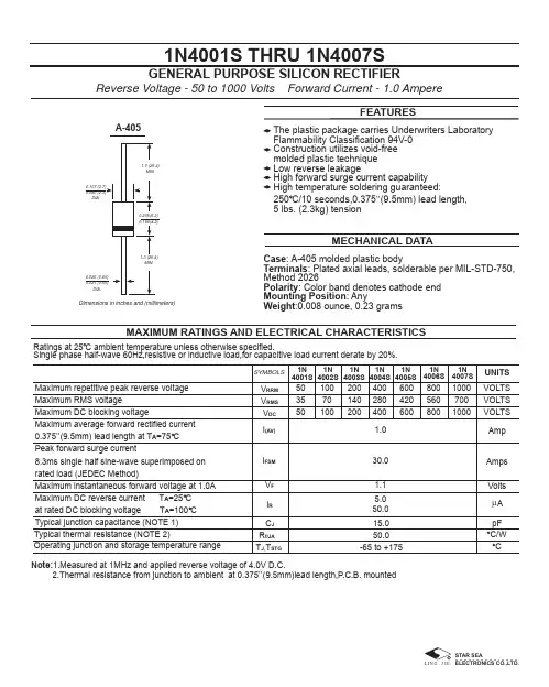
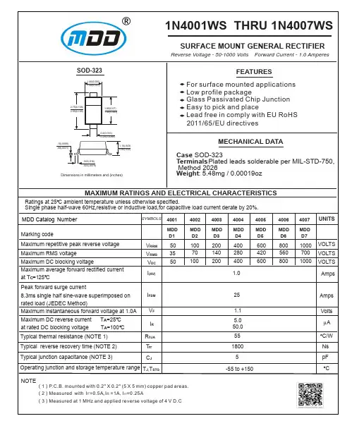
1N4001S THRU 1N4007SGENERAL PURPOSE SILICON RECTIFIERReverse Voltage - 50 to 1000 Volts Forward Current - 1.0 AmpereCase : A-405 molded plastic bodyTerminals : Plated axial leads, solderable per MIL-STD-750,Method 2026Polarity : Color band denotes cathode end Mounting Position : AnyWeight :0.008 ounce, 0.23 gramsThe plastic package carries Underwriters Laboratory Flammability Classification 94V-0Construction utilizes void-free molded plastic technique Low reverse leakageHigh forward surge current capability High temperature soldering guaranteed:250 C/10 seconds,0.375”(9.5mm) lead length,5 lbs. (2.3kg) tensionFEATURESMECHANICAL DATAMAXIMUM RATINGS AND ELECTRICAL CHARACTERISTICSA-405Dimensions in inches and (millimeters)50355010070100200140200400280400600420600800560800100070010001N4001S VOLTS VOLTS VOLTS SYMBOLSUNITS AmpAmps Volts V RRM V RMS V DC I (AV)I FSM V F 1.030.01.1Operating junction and storage temperature rangeMaximum repetitive peak reverse voltage Maximum RMS voltageMaximum DC blocking voltageMaximum average forward rectified current 0.375”(9.5mm) lead length at T A =75 C Peak forward surge current8.3ms single half sine-wave superimposed on rated load (JEDEC Method)Maximum instantaneous forward voltage at 1.0A Maximum DC reverse current T A =25 C at rated DC blocking voltage T A =100 C Typical junction capacitance (NOTE 1)Note:1.Measured at 1MHz and applied reverse voltage of 4.0V D.C.2.Thermal resistance from junction to ambient at 0.375”(9.5mm)lead length,P.C.B. mountedI R 5.050.0R θJA C J T J ,T STG50.015.0-65 to +175pF CA µTypical thermal resistance (NOTE 2)C/W 1N 4002S 1N 4004S 1N 4003S 1N 4005S 1N 4007S1N 4006S Ratings at 25 C ambient temperature unless otherwise specified.Single phase half-wave 60Hz,resistive or inductive load,for capacitive load current derate by 20%.RATINGS AND CHARACTERISTIC CURVES 1N4001S THRU 1N4007S0.6 0.8 1.0 1.2 1.4 1.50.01 0.1 1 10 1001001010.1REVERSE VOLTAGE,VOLTSt,PULSE DURATION,sec.FIG. 5-TYPICAL JUNCTION CAPACITANCEFIG. 6-TYPICAL TRANSIENT THERMAL IMPEDANCEFIG. 3-TYPICAL INSTANTANEOUS FORWARDCHARACTERISTICSNUMBER OF CYCLES AT 60 HzFIG. 2-MAXIMUM NON-REPETITIVE PEAK FORWARDFIG. 1- FORWARD CURRENT DERATING CURVEA V E R A G E F O R W A R D R E C T I F I E D C U R R E N T ,A M P E R E SI N S T A N T A N E O U S F O R W A R D C U R R E N T ,A M P E R E SJ U N C T I O N C A P A C I T A N C E ,p FP E A K F O R W A R D S U R G E C U R R E N T ,A M P E R E SINSTANTANEOUS FORWARD VOLTAGE,VOLTS1001010.10.01PERCENT OF PEAK REVERSE VOLTAGE,%FIG. 4-TYPICAL REVERSE CHARACTERISTICSI N S T A N T A N E O U S R E V E R S E C U R R E N T ,M I C R O A M P E R E ST R A N S I E N T T H E R M A L I M P E D A N C E ,C /WAMBIENT TEMPERATURE, C。
1. 介绍1n4007二极管的基本信息1N4007是一种常见的大功率长时正向工作二极管,具有较高的反向耐压能力和大电流容许值。
它是由半导体材料制成的,可以在电子电路中用来做整流器和保护器件。
2. 1N4007二极管的外观特征1N4007二极管通常呈长方体形状,外观上有两个引线,通常一个是正极,另一个是负极。
引线的颜色可能有不同的标识,但是最常见的是正极引线为黑色,负极引线为白色。
3. 1N4007二极管的标识方法1N4007二极管的包装上通常会有标识,可以通过这些标识来识别器件型号和生产厂家。
在国内,1N4007二极管的包装上会有型号,批号等信息,这些信息是非常重要的,通过这些信息我们可以追溯到器件的生产时间和生产工艺。
4. 1N4007二极管的识别方法除了包装标识,我们还可以通过一些简单的测试方法来识别1N4007二极管。
可以使用万用表来测试二极管的正反向导通情况,从而确定其正负极。
5. 1N4007二极管的应用领域1N4007二极管广泛应用于开关电源、逆变电路、恒流电源、电机控制、逆变焊机、高频电源、充放电电路以及各种仪器仪表等领域。
6. 总结1N4007二极管是一种性能稳定、应用广泛的大功率二极管,具有较好的反向耐压能力和大电流容许值,因此在电子电路中有着重要的应用价值。
通过学习1N4007二极管的标识和识别方法,可以更好地应用于实际工程中,并确保电子产品的稳定性和可靠性。
7. 1N4007二极管的性能特点1N4007二极管的主要性能特点包括:最大可逆工作电压为1000V,平均整流电流为1A,最大浪涌电流为30A,正向压降为1V。
这些性能特点使得1N4007二极管在电子电路中具有非常好的整流性能和稳定性,能够承受较大的工作电压和电流。
8. 1N4007二极管的优势与其他类型的二极管相比,1N4007二极管具有以下优势:- 较高的反向耐压能力,能够承受较大的反向电压,适用于各种高压电路的应用;- 大电流容许值,能够承受较大的正向电流,适用于大功率电路的应用;- 正向压降较小,能够减小功耗,提高电路的效率;- 结构简单,成本低廉,制造成本相对较低,广泛应用于各种电子设备和电路。
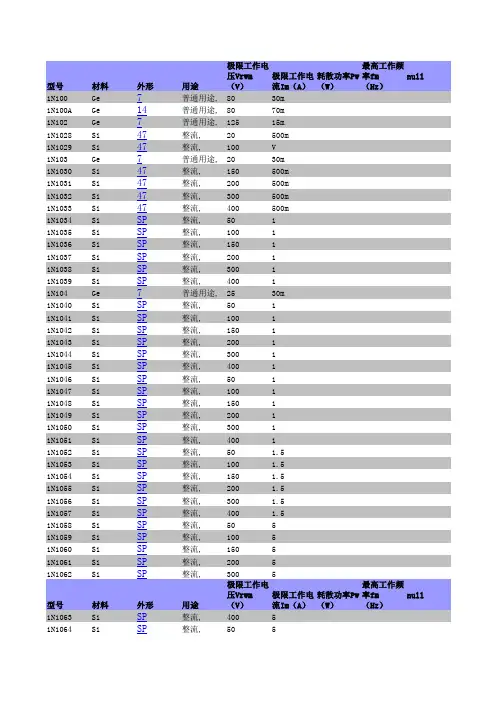
型号材料外形用途极限工作电压Vrwm(V)极限工作电流Im(A)耗散功率Pw(W)最高工作频率fm(H稳压)V稳压1N1313Si51稳压200μ150m8.75 1N1314Si51稳压200μ150m10.5 1N1315Si51稳压200μ150m12.71N1316Si51稳压200μ150m15.7 1N1317Si51稳压200μ150m18.5 1N1318Si51稳压200μ150m23.5 1N1319Si51稳压200μ150m28.5 1N1320Si51稳压200μ150m34.5 1N1321Si51稳压200μ150m41 1N1322Si51稳压200μ150m49.5 1N1323Si51稳压200μ150m58 1N1324Si51稳压200μ150m71 1N1325Si51稳压200μ150m87.5 1N1326Si51稳压200μ150m105 1N1327Si51稳压200μ150m127 1N1347Si SP整流,50061N1347A Si4整流,50061N1347B Si4整流,50061N1347C Si4整流,50061N1348Si SP整流,60061N1348A Si4整流,60061N1348B Si4整流,60061N1348C Si4整流,60061N135Ge7普通用途,755m1N1351Si4稳压500m10101N1351A Si4稳压500m1010 1N1351B Si SP稳压500m1010 1N1352Si4稳压500m10111N1352A Si4稳压500m1011 1N1352B Si SP稳压500m1011 1N1353Si4稳压500m1012 1N1353A Si4稳压500m1012 1N1353B Si稳压500m10121N1354Si4稳压500m10131N1354A Si4稳压500m1013 1N1354B Si SP稳压500m1013 1N1355Si4稳压500m10151N1355A Si4稳压500m1015 1N1355B Si SP稳压500m1015 1N1356Si4稳压500m1016 1N1356A Si4稳压500m1016 1N1356B Si SP稳压500m1016 1N1357Si4稳压500m1018 1N1357A Si4稳压500m1018 1N1357B Si SP稳压500m1018 1N1358Si4稳压150m1020 1N1358A Si4稳压150m1020 1N1358B Si SP稳压150m1020 1N1359Si4稳压150m1022 1N1359A Si4稳压150m1022 1N1359B Si SP稳压150m1022 1N1360Si4稳压150m1024 1N1360A Si4稳压150m1024 1N1360B Si SP稳压150m1024 1N1361Si4稳压150m1027 1N1361A Si4稳压150m1027 1N1361B Si SP稳压150m1027 1N1362Si4稳压150m1030 1N1362A Si4稳压150m1030 1N1362B Si SP稳压150m1030 1N1363Si4稳压150m1033 1N1363A Si4稳压150m1033 1N1363B Si SP稳压150m1033 1N1364Si4稳压150m1036 1N1364A Si4稳压150m1036 1N1364B Si SP稳压150m1036 1N1365Si4稳压150m1039 1N1365A Si4稳压150m1039 1N1365B Si SP稳压150m1039 1N1366Si4稳压150m1043 1N1366A Si4稳压150m1043 1N1366B Si SP稳压150m1043 1N1367Si4稳压150m1047 1N1367A Si4稳压150m1047 1N1367B Si SP稳压150m1047 1N1368Si4稳压150m1051 1N1368A Si4稳压150m1051 1N1368B Si稳压150m10511N1369Si4稳压150m1056 1N1369A Si4稳压150m1056 1N1369B Si SP稳压150m1056 1N1370Si4稳压50m1062 1N1370A Si4稳压50m1062 1N1370B Si SP稳压50m1062 1N1371Si4稳压50m1068 1N1371A Si4稳压50m1068 1N1371B Si SP稳压50m1068 1N1372Si4稳压50m1075 1N1372A Si4稳压50m1075 1N1372B Si SP稳压50m1075 1N1373Si4稳压50m1082 1N1373A Si4稳压50m1082 1N1373B Si SP稳压50m1082 1N1374Si4稳压50m1091 1N1374A Si4稳压50m1091 1N1374B Si SP稳压50m1091 1N1375Si4稳压50m10100 1N1375A Si4稳压50m10100 1N1376Si SP整流,502401N1377Si SP整流,1002401N1378Si SP整流,1502401N1379Si SP整流,2002401N137A Si51整流,3630m1N137B Si51整流,3675m1N1380Si SP整流,3002401N1381Si SP整流,4002401N1382Si SP整流,5002401N138A Si51整流,1850m1N138B Si51整流,189.0m1N139Ge7普通用途,4670m1N1396Si SP整流,5070 1N1397Si SP整流,10070 1N1398Si SP整流,15070 1N1399Si SP整流,200701N140Ge7普通用途,6085m1N1400Si整流,300701N1401Si SP整流,40070 1N1402Si SP整流,50070 1N1403Si SP整流,60070 1N1406Si45整流,600125m型号材料外形用途极限工作电压Vrwm(V)极限工作电流Im(A)耗散功率Pw(W)最高工作频率fm(Hz)Vz1N1911Si47整流,400 1.59页</< html>9a页</< html>12页</<。
常用开关二极管型号及主要参数开关二极管是电子元器件的一种,主要用于电路中的开关控制功能。
按照功能来说,开关二极管可以分为开关二极管和反向恢复二极管两种。
开关二极管通常用于低压电路中的开关控制电路,其主要参数有正向电压、反向电压、正向电流和反向电容等。
常用开关二极管型号1. 1N41481N4148是一种快速开关二极管,常用于高速开关电路和频繁开关电路的应用中。
其正向电压为100V,正向电流为300mA。
在开关频率高于1MHz时,其开关速度优于其他开关二极管。
2. 1N40071N4007是一种一般用途整流二极管,常用于低压电路中。
其正向电压为1000V,正向电流为1A。
由于其价格较低、结构简单,因此被广泛使用。
3. 1N58191N5819是一种快速恢复二极管,常用于功率电路中的开关控制电路。
其正向电压为40V,正向电流为1A。
由于其反向恢复时间短,可在高频开关电路中发挥较好的性能。
开关二极管的主要参数1. 正向电压正向电压是指正向工作时二极管的最大电压值,通常以Vf表示。
在超过正向电压时,二极管会开始导通。
2. 反向电压反向电压是指反向工作时二极管的最大电压值,通常以Vr表示。
在超过反向电压时,二极管会瞬时击穿并开始导通。
3. 正向电流正向电流是指正向工作时二极管的最大电流值,通常以If表示。
当二极管导通时,其正向电流会逐渐增大,并受到管子本身的导通能力和电路的限制。
4. 反向电容反向电容是指反向工作时二极管的电容值,通常以Cr表示。
反向电容主要由管子的内部结构以及与终端接触的材料等因素决定。
对于高频开关电路,反向电容应尽量小。
开关二极管是电子中不可或缺的元器件之一,其性能指标决定了电路的稳定性和可靠性。
以上介绍了三种常用的开关二极管型号及其主要参数,可根据实际需求进行选择和应用。
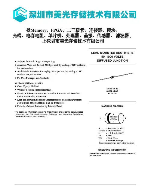
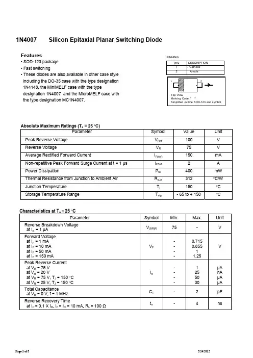
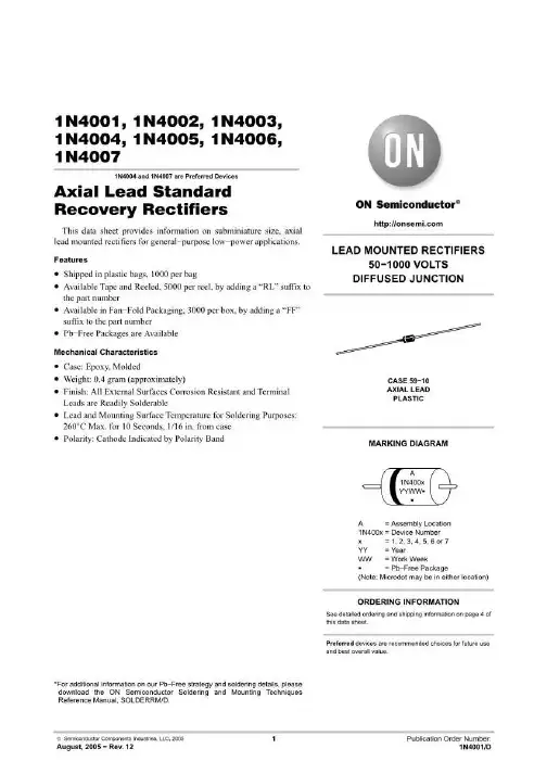
1N4001, 1N4002, 1N4003,1N4004, 1N4005, 1N4006,1N40071N4004 and 1N4007 are Preferred DevicesAxial Lead Standard Recovery RectifiersThis data sheet provides information on subminiature size, axial lead mounted rectifiers for general−purpose low−power applications. Features•Shipped in plastic bags, 1000 per bag•Available Tape and Reeled, 5000 per reel, by adding a “RL” suffix to the part number•Available in Fan−Fold Packaging, 3000 per box, by adding a “FF”suffix to the part number•Pb−Free Packages are AvailableMechanical Characteristics•Case: Epoxy, Molded•Weight: 0.4 gram (approximately)•Finish: All External Surfaces Corrosion Resistant and Terminal Leads are Readily Solderable•Lead and Mounting Surface Temperature for Soldering Purposes: 260°C Max. for 10 Seconds, 1/16 in. from case •Polarity: Cathode Indicated by Polarity Band*For additional information on our Pb−Free strategy and soldering details, please download the ON Semiconductor Soldering and Mounting Techniques Reference Manual, SOLDERRM/D.CASE 59−10AXIAL LEADPLASTICLEAD MOUNTED RECTIFIERS50−1000 VOLTSDIFFUSED JUNCTIONPreferred devices are recommended choices for future use and best overall value.MARKING DIAGRAMSee detailed ordering and shipping information on page 4 of this data sheet.ORDERING INFORMATIONA= Assembly Location1N400x= Device Numberx= 1, 2, 3, 4, 5, 6 or 7YY= YearWW= Work WeekG= Pb−Free Package(Note: Microdot may be in either location)A1N400xYYWW GGMAXIMUM RATINGSRating Symbol1N40011N40021N40031N40041N40051N40061N4007Unit†Peak Repetitive Reverse Voltage Working Peak Reverse Voltage DC Blocking Voltage V RRMV RWMV R501002004006008001000V†Non−Repetitive Peak Reverse Voltage(halfwave, single phase, 60 Hz)V RSM6012024048072010001200V †RMS Reverse Voltage V R(RMS)3570140280420560700V†Average Rectified Forward Current(single phase, resistive load,60 Hz, T A = 75°C)I O 1.0A†Non−Repetitive Peak Surge Current(surge applied at rated load conditions)I FSM30 (for 1 cycle)AOperating and Storage Junction Temperature RangeT JT stg−65 to +175°CMaximum ratings are those values beyond which device damage can occur. Maximum ratings applied to the device are individual stress limit values (not normal operating conditions) and are not valid simultaneously. If these limits are exceeded, device functional operation is not implied, damage may occur and reliability may be affected.ELECTRICAL CHARACTERISTICS†Rating Symbol Typ Max Unit Maximum Instantaneous Forward Voltage Drop, (i F = 1.0 Amp, T J = 25°C)v F0.93 1.1V Maximum Full−Cycle Average Forward Voltage Drop, (I O = 1.0 Amp, T L = 75°C, 1 inch leads)V F(AV)−0.8VMaximum Reverse Current (rated DC voltage) (T J = 25°C)(T J = 100°C)I R0.051.01050m AMaximum Full−Cycle Average Reverse Current, (I O = 1.0 Amp, T L = 75°C, 1 inch leads)I R(AV)−30m A †Indicates JEDEC Registered Data10.110I F , F O R W A R D C U R R E N T (A )Figure 3. Typical CapacitanceV R , REVERSE VOLTAGE (V)1N4001Axial Lead*1000 Units/Bag1N4001G Axial Lead*1000 Units/Bag(Pb−Free)1N4001FF Axial Lead*3000 Units/Box3000 Units/Box1N4001FFG Axial Lead*(Pb−Free)1N4001RL Axial Lead*5000/T ape & Reel5000/T ape & Reel1N4001RLG Axial Lead*(Pb−Free)1N4002Axial Lead*1000 Units/Bag1000 Units/Bag1N4002G Axial Lead*(Pb−Free)1N4002FF Axial Lead*3000 Units/Box3000 Units/Box1N4002FFG Axial Lead*(Pb−Free)1N4002RL Axial Lead*5000/T ape & Reel5000/T ape & Reel1N4002RLG Axial Lead*(Pb−Free)1N4003Axial Lead*1000 Units/Bag1N4003G Axial Lead*1000 Units/Bag(Pb−Free)1N4003FF Axial Lead*3000 Units/Box3000 Units/Box1N4003FFG Axial Lead*(Pb−Free)1N4003RL Axial Lead*5000/T ape & Reel5000/T ape & Reel1N4003RLG Axial Lead*(Pb−Free)1N4004Axial Lead*1000 Units/Bag1000 Units/Bag1N4004G Axial Lead*(Pb−Free)1N4004FF Axial Lead*3000 Units/Box3000 Units/Box1N4004FFG Axial Lead*(Pb−Free)1N4004RL Axial Lead*5000/T ape & Reel5000/T ape & Reel1N4004RLG Axial Lead*(Pb−Free)1N4005Axial Lead*1000 Units/Bag1N4005G Axial Lead*1000 Units/Bag(Pb−Free)1N4005FF Axial Lead*3000 Units/Box3000 Units/Box1N4005FFG Axial Lead*(Pb−Free)1N4005RL Axial Lead*5000/T ape & Reel5000/T ape & Reel1N4005RLG Axial Lead*(Pb−Free)†For information on tape and reel specifications, including part orientation and tape sizes, please refer to our Tape and Reel Packaging Specifications Brochure, BRD8011/D.*This package is inherently Pb−Free.1N4006Axial Lead*1000 Units/Bag1000 Units/Bag1N4006G Axial Lead*(Pb−Free)1N4006FF Axial Lead*3000 Units/Box3000 Units/Box1N4006FFG Axial Lead*(Pb−Free)1N4006RL Axial Lead*5000/T ape & Reel1N4006RLG Axial Lead*5000/T ape & Reel(Pb−Free)1N4007Axial Lead*1000 Units/Bag1000 Units/Bag1N4007G Axial Lead*(Pb−Free)1N4007FF Axial Lead*3000 Units/Box3000 Units/Box1N4007FFG Axial Lead*(Pb−Free)1N4007RL Axial Lead*5000/T ape & Reel1N4007RLG Axial Lead*5000/T ape & Reel(Pb−Free)†For information on tape and reel specifications, including part orientation and tape sizes, please refer to our Tape and Reel Packaging Specifications Brochure, BRD8011/D.*This package is inherently Pb−Free.PACKAGE DIMENSIONSAXIAL LEAD CASE 59−10ISSUE UDIM MIN MAX MIN MAX MILLIMETERSINCHES A 4.10 5.200.1610.205B 2.00 2.700.0790.106D 0.710.860.0280.034F −−− 1.27−−−0.050K25.40−−−1.000−−−NOTES:1.DIMENSIONING AND TOLERANCING PER ANSI Y14.5M, 1982.2.CONTROLLING DIMENSION: INCH.3.ALL RULES AND NOTES ASSOCIATED WITH JEDEC DO−41 OUTLINE SHALL APPLY4.POLARITY DENOTED BY CATHODE BAND.5.LEAD DIAMETER NOT CONTROLLED WITHIN F DIMENSION.ON Semiconductor and are registered trademarks of Semiconductor Components Industries, LLC (SCILLC). SCILLC reserves the right to make changes without further noticeto any products herein. SCILLC makes no warranty, representation or guarantee regarding the suitability of its products for any particular purpose, nor does SCILLC assume any liability arising out of the application or use of any product or circuit, and specifically disclaims any and all liability, including without limitation special, consequential or incidental damages.“Typical” parameters which may be provided in SCILLC data sheets and/or specifications can and do vary in different applications and actual performance may vary over time. All operating parameters, including “Typicals” must be validated for each customer application by customer’s technical experts. SCILLC does not convey any license under its patent rights nor the rights of others. SCILLC products are not designed, intended, or authorized for use as components in systems intended for surgical implant into the body, or other applications intended to support or sustain life, or for any other application in which the failure of the SCILLC product could create a situation where personal injury or death may occur. Should Buyer purchase or use SCILLC products for any such unintended or unauthorized application, Buyer shall indemnify and hold SCILLC and its officers, employees, subsidiaries, affiliates,and distributors harmless against all claims, costs, damages, and expenses, and reasonable attorney fees arising out of, directly or indirectly, any claim of personal injury or death associated with such unintended or unauthorized use, even if such claim alleges that SCILLC was negligent regarding the design or manufacture of the part. SCILLC is an Equal Opportunity/Affirmative Action Employer. This literature is subject to all applicable copyright laws and is not for resale in any manner.PUBLICATION ORDERING INFORMATION分销商库存信息:ONSEMI1N4007RLG1N4002RLG1N4004RLG 1N4005RLG1N4003RLG1N4001RLG 1N4004G1N4007G1N4001G1N4002G1N4003G1N4006G1N4005G1N4001RL1N4002RL 1N4003RL1N4004RL1N4005RL 1N4006RL1N4006RLG1N4007RL。
Features
1N4001/L - 1N4007/L
1.0A RECTIFIER
“L” Suffix Designates A-405 Package No Suffix Designates DO-41 Package A
A
B C
D
DO-41 Plastic
A-405Dim Min Max Min Max A 25.40¾25.40¾B 4.06 5.21 4.10 5.20C 0.710.8640.530.64D
2.00
2.72
2.00
2.70
All Dimensions in mm
Maximum Ratings and Electrical Characteristics
@ T A = 25°C unless otherwise specified
·Diffused Junction
·High Current Capability and Low Forward Voltage Drop
·Surge Overload Rating to 30A Peak ·Low Reverse Leakage Current ·
Plastic Material: UL Flammability Classification Rating 94V-0
Mechanical Data
·Case: Molded Plastic
·Terminals: Plated Leads Solderable per MIL-STD-202, Method 208·Polarity: Cathode Band
·Weight: DO-41 0.30 grams (approx)
A-405 0.20 grams (approx)
·Mounting Position: Any ·
Marking: Type Number
Single phase, half wave, 60Hz, resistive or inductive load.For capacitive load, derate current by 20%.
Characteristic
Symbol 1N 4001/L 1N 4002/L 1N 4003/L 1N 4004/L
1N 4005/L 1N 4006/L 1N 4007/L Unit Peak Repetitive Reverse Voltage Working Peak Reverse Voltage DC Blocking Voltage V RRM
V RWM V R 501002004006008001000V RMS Reverse Voltage
V R(RMS)
35
70
140
280420
560
700
V Average Rectified Output Current (Note 1)@ T A = 75°C I O 1.0A Non-Repetitive Peak Forward Surge Current 8.3ms single half sine-wave superimposed on rated load (JEDEC Method)I FSM 30A Forward Voltage
@ I F = 1.0A V FM 1.0V Peak Reverse Current
@ T A = 25°C at Rated DC Blocking Voltage @ T A = 100°C
I RM 5.050
m A Typical Junction Capacitance (Note 2)
C j 15
8
pF Typical Thermal Resistance Junction to Ambient R q JA 100K/W Maximum DC Blocking Voltage Temperature T A +150°C Operating and Storage Temperature Range (Note 3)
T j,T STG
-65 to +175
°C
Notes:
1. Leads maintained at ambient temperature at a distance of 9.5mm from the case.
2. Measured at 1.MHz and applied reverse voltage of 4.0V DC.
3. JEDEC Value .
406080100120140160180
0.2
0.4
0.6
0.8
1.0
I ,A V E R A G E F O R W A R D R E C T I F I E D C U R R E N T (A )
(A V )T ,AMBIENT TEMPERATURE (ºC)Fig.1Forward Current Derating Curve
A C ,C A P A C I T A N C E (p F )
j V ,REVERSE VOLTAGE (V)Fig.4Typical Junction Capacitance
R 1.010
100
1.0
10
100
1.0
10100
I ,P E A
K F O R W A R D S U R G E C U R R E N T (A )
F S M NUMBER OF CYCLES AT 60Hz
Fig.3Max Non-Repetitive Peak Fwd Surge Current
40
30
20
010
500.6
0.8 1.0 1.2 1.4 1.6
0.01
0.1
1.0
I ,I N S T A
N T A N E O U S F O R W A R D C U R R E N T (A )
F V ,INSTANTANEOUS FORWARD VOLTAGE (V)
Fig.2Typical Forward Characteristics
F 10。