硅片行业术语大全中英文对照I-Z
- 格式:docx
- 大小:68.57 KB
- 文档页数:12
1.•Vt could drops or c limbs as gate length shrinks à Short Channel Effect or Reverse Short Channel Effect.2•Vt could drops or climbs as AA width shrinks àNarrow width Effect or Reverse Narrow Width Effect.3•Channel profile determines SCE and RSCE.4•Isolation structure and channel profile determines NWE and RNWE.ASIC: 专用集成电路application specific ICW/S:width/spaceSTI: shallow slot isolationSlurry泥浆, 浆Pad 衬垫RTI 实时检测SC specially characteristic 关键属性Numerical Aperture(N.A.)數值孔徑LDD: low dose drain 轻掺杂漏极: to supperess the SCEATPG:auto test pattern generatorADI: After Developing InspectionDIBL (Drain Induced Barrier Lowering)GIDL(gate induced drain leakage)PSM phase-shift mask 相移掩膜技术SC1 standard clean 1SC2 standard clean 2FEOL front-end of lineBEOL back-end of lineDIBL: drain induced barrier lowerGIDL: drain induced drain leakageSCE: short channel effectSAC oxide: sacrifice oxideDARC: dielectric anti-reflective coating 无机物; barc & tarc bottom and top 有机物SDE:source/drain-extensionRCA : SC1 + SC2Caro:3号液:PRRM: PhotoResist ReMoveEKC : EKC 270T (solvent name)APM,SPM,HPM的主要成分,除何种杂质;HF的作用。
一、硅片行业术语大全(中英文对照A-H)Acceptor - An element, such as boron, indium, and gallium used to create a free hole in a semiconductor. The acceptor atoms are required to have one less valence electron than the semiconductor.受主- 一种用来在半导体中形成空穴的元素,比如硼、铟和镓。
受主原子必须比半导体元素少一价电子Alignment Precision - Displacement of patterns that occurs during the photolithography process.套准精度- 在光刻工艺中转移图形的精度。
Anisotropic - A process of etching that has very little or no undercutting各向异性- 在蚀刻过程中,只做少量或不做侧向凹刻。
Area Contamination - Any foreign particles or material that are found on the surface of a wafer. This is viewed as discolored or smudged, and it is the result of stains, fingerprints, water spots, etc.沾污区域- 任何在晶圆片表面的外来粒子或物质。
由沾污、手印和水滴产生的污染。
Azimuth, in Ellipsometry - The angle measured between the plane of incidence and the major axis of the ellipse.椭圆方位角- 测量入射面和主晶轴之间的角度。
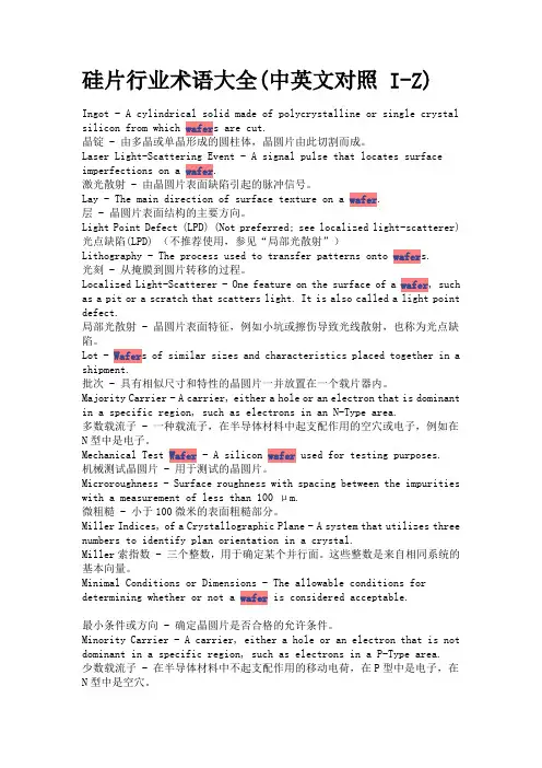
硅片行业术语大全(中英文对照 I—Z)Ingot — A cylindrical solid made of polycrystalline or single crystal silicon from which wafer s are cut。
晶锭—由多晶或单晶形成的圆柱体,晶圆片由此切割而成.Laser Light—Scattering Event — A signal pulse that locates surface imperfections on a wafer。
激光散射 - 由晶圆片表面缺陷引起的脉冲信号。
Lay — The main direction of surface texture on a wafer。
层—晶圆片表面结构的主要方向。
Light Point Defect (LPD)(Not preferred; see localized light-scatterer) 光点缺陷(LPD)(不推荐使用,参见“局部光散射")Lithography — The process used to transfer patterns onto wafer s.光刻—从掩膜到圆片转移的过程。
Localized Light—Scatterer —One feature on the surface of a wafer, such as a pit or a scratch that scatters light. It is also called a light point defect。
局部光散射—晶圆片表面特征,例如小坑或擦伤导致光线散射,也称为光点缺陷。
Lot —Wafer s of similar sizes and characteristics placed together in a shipment。
批次—具有相似尺寸和特性的晶圆片一并放置在一个载片器内.Majority Carrier - A carrier, either a hole or an electron that is dominant in a specific region, such as electrons in an N—Type area。
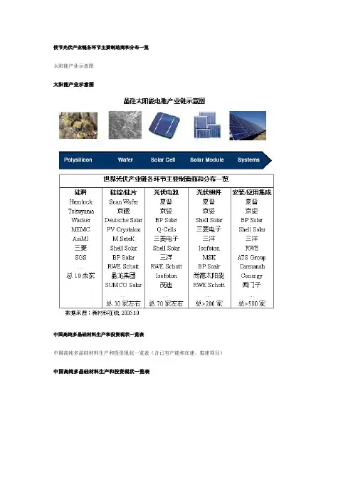
使节光伏产业链各环节主要制造商和分布一览太阳能产业示意图太阳能产业示意图中国高纯多晶硅材料生产和投资现状一览表中国高纯多晶硅材料生产和投资现状一览表(含已有产能和在建、拟建项目)中国高纯多晶硅材料生产和投资现状一览表国外硅片供应商大全国外硅片供应商大全(转载)/sites/start/start.htm /default.asphttp://www.rasa.co.jp硅片行业术语大全Acceptor - An element, such as boron, indium, and gallium used to create a free hole in a semiconductor. The acceptor atoms are required to have one less valence electron than the semiconductor.受主- 一种用来在半导体中形成空穴的元素,比如硼、铟和镓。
受主原子必须比半导体元素少一价电子Alignment Precision - Displacement of patterns that occurs during the photolithography process. 套准精度- 在光刻工艺中转移图形的精度。
Anisotropic - A process of etching that has very little or no undercutting各向异性- 在蚀刻过程中,只做少量或不做侧向凹刻。
Area Contamination - Any foreign particles or material that are found on the surface of a wafer. This is viewed as discolored or smudged, and it is the result of stains, fingerprints, water spots, etc. 沾污区域- 任何在晶圆片表面的外来粒子或物质。
分享举报| 硅片行业术语大全(中英文对照 I-Z)热9徐静文 2009-12-31 15:03硅片行业术语大全(中英文对照 I-Z)硅片行业术语大全(中英文对照 I-Z)In got - A cy lindr icalsolid made of p olycr ystal lineor si nglecryst al si licon from whic h waf ers a re cu t.晶锭 - 由多晶或单晶形成的圆柱体,晶圆片由此切割而成。
L aserLight-Scat terin g Eve nt -A sig nal p ulsethatlocat es su rface impe rfect ionson awafer.激光散射 -由晶圆片表面缺陷引起的脉冲信号。
La y - T he ma in di recti on of surf ace t extur e ona waf er. 层 - 晶圆片表面结构的主要方向。
L ightPoint Defe ct (L PD) (Not p refer red;see l ocali zed l ight-scatt erer)光点缺陷(LPD) (不推荐使用,参见“局部光散射”)Lith ograp hy -The p roces s use d totrans fer p atter ns on to wa fers.光刻- 从掩膜到圆片转移的过程。
Loca lized Ligh t-Sca ttere r - O ne fe ature on t he su rface of a wafe r, su ch as a pi t orascr atchthatscatt ers l ight. It i s als o cal led a ligh t poi nt de fect.局部光散射 -晶圆片表面特征,例如小坑或擦伤导致光线散射,也称为光点缺陷。
silicon profile翻译硅材料简介硅是一种广泛使用的半导体材料,其化学符号为Si。
它是地壳中第二丰富的元素,占地壳总质量的约27%。
硅具有很高的热导率和电导率,因此被广泛用于制造电子器件和太阳能电池等应用中。
硅材料的用途广泛,以下是一些常见的应用和中英文对照例句:1. 电子器件制造:硅是制造集成电路和晶体管等电子器件的基本材料。
- Silicon wafers are used as substrates for manufacturing microchips. (硅晶圆用作微芯片的基片。
)- Silicon-based transistors revolutionized the field of electronics. (基于硅的晶体管彻底改变了电子领域。
)2. 太阳能电池:硅材料是太阳能电池的主要组成部分,用于将太阳能转化为电能。
- Silicon solar cells are widely used in renewable energy systems. (硅太阳能电池广泛应用于可再生能源系统中。
)- The efficiency of silicon-based solar panels has greatly improved in recent years. (基于硅的太阳能电池板的效率近年来有了很大提升。
)3. 光学材料:硅具有良好的透明性和光学特性,被用于制造光学器件和光纤等。
- Silicon lenses are used in cameras and optical instruments. (硅透镜用于相机和光学仪器中。
)- Silicon-based optical fibers are widely used for high-speed data transmission. (基于硅的光纤广泛用于高速数据传输。
)4. 化工行业:硅材料可以制备许多化学品和合成材料。
多晶硅技术英语词汇(原创)
English-Chinese Glossary List for PCS Technology
多晶硅技术涉及冶金、半导体材料、化工、机械、热能、电子等各个专业的交叉,在国外多晶硅行业对其中的许多专有词汇有专门的说法,国内目前还没有多晶硅专业词汇出版,以致国内的业界人士在进行多晶硅项目国际合作时使用了很多Chinese English,造成沟通上的误解。
博主通过近几年和国外同行大量的交流,将多晶硅行业专用的英语词汇进行了整理,供业内的朋友参考使用。
由于时间关系,本词汇先粗略发布,日后会不断地充实完善。
硅片行业术语大全(中英文对照I-Z)硅片行业术语大全(中英文对照I-Z)Ingot - A cylindrical solid made of polycrystalline or single crystal silicon from which wafers are cut.晶锭- 由多晶或单晶形成的圆柱体,晶圆片由此切割而成。
Laser Light-Scattering Event - A signal pulse that locates surface imperfections on a wafer. 激光散射- 由晶圆片表面缺陷引起的脉冲信号。
Lay - The main direction of surface texture on a wafer.层- 晶圆片表面结构的主要方向。
Light Point Defect (LPD) (Not preferred; see localized light-scatterer)光点缺陷(LPD) (不推荐使用,参见“局部光散射”)Lithography - The process used to transfer patterns onto wafers.光刻- 从掩膜到圆片转移的过程。
Localized Light-Scatterer - One feature on the surface of a wafer, such as a pit or a scratch that scatters light. It is also called a light point defect.局部光散射- 晶圆片表面特征,例如小坑或擦伤导致光线散射,也称为光点缺陷。
Lot - Wafers of similar sizes and characteristics placed together in a shipment.批次- 具有相似尺寸和特性的晶圆片一并放置在一个载片器内。
硅片行业术语大全(中英文对照 I-Z)Ingot - A cylindrical solid made of polycrystalline or single crystal silicon from which wafer s are cut.晶锭 - 由多晶或单晶形成的圆柱体,晶圆片由此切割而成。
Laser Light-Scattering Event - A signal pulse that locates surface imperfections on a wafer.激光散射 - 由晶圆片表面缺陷引起的脉冲信号。
Lay - The main direction of surface texture on a wafer.层 - 晶圆片表面结构的主要方向。
Light Point Defect (LPD) (Not preferred; see localized light-scatterer) 光点缺陷(LPD) (不推荐使用,参见“局部光散射”)Lithography - The process used to transfer patterns onto wafer s.光刻 - 从掩膜到圆片转移的过程。
Localized Light-Scatterer - One feature on the surface of a wafer, such as a pit or a scratch that scatters light. It is also called a light point defect.局部光散射 - 晶圆片表面特征,例如小坑或擦伤导致光线散射,也称为光点缺陷。
Lot - Wafer s of similar sizes and characteristics placed together in a shipment.批次 - 具有相似尺寸和特性的晶圆片一并放置在一个载片器内。
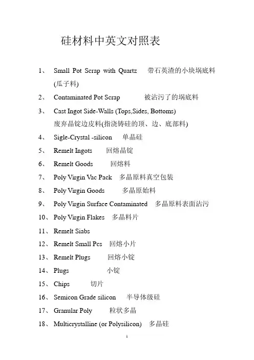
硅材料中英文对照表1、Small Pot Scrap with Quartz 带石英渣的小块埚底料(瓜子料)2、Contaminated Pot Scrap 被沾污了的埚底料3、Cast Ingot Side-Walls (Tops,Sides, Bottoms)废弃晶锭边皮料(指浇铸硅的顶、边、底部料)4、Sigle-Crystal -silicon 单晶硅5、Remelt Ingots 回熔晶锭6、Remelt Goods 回熔料7、Poly Virgin Vac Pack 多晶原料真空包装8、Poly Virgin Goods 多晶原始料9、Poly Virgin Surface Contaminated 多晶原料表面沾污10、Poly Virgin Flakes 多晶料片11、Remelt Siabs12、Remelt Small Pcs 回熔小片13、Remelt Plugs 回熔小锭14、Plugs 小锭15、Chips 切片16、Semicon Grade silicon 半导体级硅17、Granular Poly 粒状多晶18、Multicrystalline (or Polysilicon) 多晶硅19、Recliam Wafers 回收硅片20、Broken Cells 碎电池片21、N-type N型22、P-type P型23、Resistivity (ohm-cm ) 电阻率(欧姆-厘米)24、Orintation 晶向25、Beam 横樑料26、Polysilicon with Carbon (or Graphite) 碳头料27、Solar Grade Silicon 太阳能级硅28、Minor Carrier life-time 少数载流子寿命29、Acceptor Impurity 受主杂质。
又称P型杂质(如硅中的硼、铝、镓、铟等杂质),这是指为半导体材料提供空穴的一类杂质。
半导体厂务专业名词中英文对照表Semiconductor Factory Terminologies English-Chinese Comparison1. Semiconductor - 半导体2. Wafer - 晶圆3. Die - 芯片4. Clean Room - 净化室5. Lithography - 光刻6. Etching - 蚀刻7. Deposition - 沉积8. Patterning - 图形化9. Doping - 掺杂10. Metrology - 计量11. Inspection - 检验12. Test - 测试13. Assembly - 组装14. Packaging - 封装15. Back-End - 后端16. Front-End - 前端17. Sputtering - 粒子沉积18. Chemical Vapor Deposition (CVD) - 化学气相沉积19. Physical Vapor Deposition (PVD) - 物理气相沉积20. Thin Film - 薄膜21. Photolithography - 光刻技术22. Ion Implantation - 离子注入23. Diffusion - 扩散24. Planarization - 平坦化25. Ion Etching - 离子蚀刻26. Circuit - 电路27. Integrated Circuit (IC) - 集成电路28. Silicon - 硅29. Gallium Arsenide (GaAs) - 砷化镓30. Silicon dioxide - 二氧化硅This English-Chinese comparison table provides a comprehensive list of key terminologies used in the semiconductor industry. These terms are essential for professionals working in semiconductor manufacturing facilities to communicate effectively with their Chinese counterparts. From basic concepts like wafer and die to advanced processes such as lithography and etching, having a clear understanding of these terms in both languages is crucial for successful collaboration and operations in a semiconductor factory.。
光伏行业英文词汇Cell 电池Crystalline silicon 晶体硅Photovoltaic 光伏bulk properties 体特性at ambient temperature 在室温下wavelength 波长absorption coefficient 吸收系数electron-hole pairs 电子空穴对photon 光子density 密度defect 缺陷surface 表面electrode 电极p-type for hole extraction p型空穴型n-type for electron extraction n 型电子型majority carriers 多数载流子minority carriers 少数载流子surface recombination velocity (SRV)表面复合速率back surface field (BSF)背场at the heavily doped regions 重掺杂区saturation current density Jo 饱和电流密度thickness 厚度contact resistance 接触电阻concentration 浓度boron 硼Gettering techniques吸杂nonhomogeneous 非均匀的solubility 溶解度selective contacts 选择性接触insulator 绝缘体oxygen 氧气hydrogen 氢气Plasma enhanced chemical vapor deposition PECVDInterface 界面The limiting efficiency 极限效率reflection 反射light- trapping 光陷intrinsic material 本征材料bifacial cells 双面电池monocrystalline 单晶float zone material FZ-Si Czochralski silicon Cz-Si industrial cells 工业电池a high concentration of oxygen 高浓度氧Block or ribbon 块或硅带Crystal defects 晶体缺陷grain boundaries 晶界dislocation 位错solar cell fabrication 太阳能电池制造impurity 杂质P gettering effect 磷吸杂效果Spin-on 旋涂supersaturation 过饱和dead layer 死层electrically inactive phosphorus 非电活性磷interstitial 空隙the eutectic temperature 共融温度boron-doped substrate 掺硼基体passivated emitter and rear locally diffused cells PERL电池losses 损失the front surface 前表面metallization techniques 金属化技术metal grids 金属栅线laboratory cells 实验室电池the metal lines 金属线selective emitter 选择性发射极photolithographic 光刻gradient 斜度precipitate 沉淀物localized contacts 局部接触point contacts 点接触passivated emitter rear totally diffused PERTsolder 焊接bare silicon 裸硅片high refraction index 高折射系数reflectance 反射encapsulation 封装antireflection coating ARC减反射层an optically thin dielectric layer 光学薄电介层interference effects 干涉效应texturing 制绒alkaline solutions 碱溶液etch 刻蚀/腐蚀anisotropically 各向异性地plane 晶面pyramids 金字塔a few microns 几微米etching time and temperature 腐蚀时间和温度manufacturing process 制造工艺process flow 工艺流程high yield 高产量starting material 原材料solar grade 太阳级a pseudo-square shape 单晶型状saw damage removal 去除损伤层fracture 裂纹acid solutions 酸溶液immerse 沉浸tank 槽texturization 制绒microscopic pyramids 极小的金字塔size 尺寸大小hinder the formation of the contacts 阻碍电极的形成the concentration,the temperature and the agitation of the solution 溶液的浓度,温度和搅拌the duration of the bath 溶液维持时间alcohol 酒精improve 改进增加homogeneity 同质性wettability 润湿性phosphorus diffusion 磷扩散eliminate adsorbed metallic impurities 消除吸附的金属杂质quartz furnaces 石英炉quartz boats 石英舟quartz tube 石英炉管bubbling nitrogen through liquid POCL3 小氮belt furnaces 链式炉back contact cell 背电极电池reverse voltage 反向电压reverse current 反向电流amorphous glass of phospho-silicates 非晶玻璃diluted HF 稀释HF溶液junction isolation 结绝缘coin-stacked 堆放barrel-type reactors 桶状反应腔fluorine 氟fluorine compound 氟化物simultaneously 同时地high throughput 高产出ARC deposition 减反层沉积Titanium dioxide TiO2Refraction index 折射系数Encapsulated cell 封装电池Atmospheric pressure chemical vapor deposition APCVDSprayed from a nozzle 喷嘴喷雾Hydrolyze 水解Spin -on 旋涂Front contact print 正电极印刷The front metallization 前面金属化Low contact resistance to silicon 低接触电阻Low bulk resistivity 低体电阻率Low line width with high aspect ratio 低线宽高比Good mechanical adhesion 好机械粘贴solderability 可焊性screen printing 丝网印刷comblike pattern 梳妆图案finger 指条bus bars 主栅线viscous 粘的solvent 溶剂back contact print 背电极印刷both silver and aluminum 银铝form ohmic contact 形成欧姆接触warp 弯曲cofiring of metal contacts 电极共烧organic components of the paste 浆料有机成分burn off 烧掉sinter 烧结perforate 穿透testing and sorting 测试分选I-V curve I-V曲线Module 组件Inhomogeneous 不均匀的Gallium 镓Degradation 衰减A small segregation coefficient 小分凝系数Asymmetric 不对称的High resolution 高分辨率Base resistivity 基体电阻率The process flow 工艺流程Antireflection coating 减反射层Cross section of a solar cell 太阳能电池横截面Dissipation 损耗Light-generated current 光生电流Incident photons 入射光子The ideal short circuit flow 理想短路电路The depletion region 耗尽区Quantum efficiency 量子效率Blue response 蓝光效应Spectral response 光谱响应Light-generated carriers 光生载流子Forward bias 正向偏压Simulation 模拟Equilibrium 平衡Superposition 重合The fourth quadrant 第四象限The saturation current 饱和电流Io Fill factor 填充因子FF Graphically 用图象表示The maximum theoretical FF 理论上Empirically 经验主义的Normalized Voc 规范化VocThe ideality factor n-factor 理想因子Terrestrial solar cells 地球上的电池At a temperature of 25C 25度下Under AM1.5 conditions 在AM1.5环境下Efficiency is defined as ××定义为Fraction 分数Parasitic resistances 寄生电阻Series resistance 串联电阻Shunt resistance 并联电阻The circuit diagram 电路图Be sensitive to temperature 易受温度影响The band gap of a semiconductor 半导体能隙The intrinsic carrier concentration 本征载流子的浓度Reduce the optical losses 减少光损Deuterated silicon nitride 含重氢氮化硅Buried contact solar cells BCSC Porous silicon PS 多孔硅Electrochemical etching 电化学腐蚀Screen printed SP 丝网印刷A sheet resistance of 45-50 ohm/sq 45到50方块电阻The reverse saturation current density Job 反向饱和电流密度Destructive interference 相消干涉Surface textingInverted pyramid 倒金字塔Four point probe 四探针Saw damage etchAlkaline 碱的Cut groove 开槽Conduction band 导带Valence band 价带B and O simultaneously in silicon 硼氧共存Iodine/methanol solution 碘酒/甲醇溶液Rheology 流变学Spin-on dopants 旋涂掺杂Spray-on dopants 喷涂掺杂The metallic impurities 金属杂质One slot for two wafers 一个槽两片Throughput 产量A standard POCL3 diffusion 标准POCL3扩散Back-to-back diffusion 背靠背扩散Heterojunction with intrinsic thin -layer HIT电池Refine 提炼Dye sensitized solar cell 染料敏化太阳电池Organic thin film solar cell 有机薄膜电池Infra red 红外光Unltra violet 紫外光Parasitic resistance 寄生电阻Theoretical efficiency 理论效率Busbar 主栅线Kerf loss 锯齿损失Electric charge 电荷Covalent bonds 共价键The coefficient of thermal expansion (CTE) 热膨胀系数Bump 鼓泡Alignment 基准Fiducial mark 基准符号Squeegee 橡胶带Isotropic plasma texturing 各向等离子制绒Block-cast multicrystalline silicon 整铸多晶硅Parasitic junction removal 寄生结的去除Iodine ethanol 碘酒Deionised water 去离子水Viscosity 粘性Mesh screen 网孔Emulsion 乳胶Properties of light 光特性Electromagnetic radiation 电磁辐射The visible light 可见光The wavelength,denoted by R 用R 表示波长An inverse relationship between……and……given by the equation:相反关系,可用方程表示Spectral irradiance 分光照度……is shown in the figure below. Directly convert electricity into sunlight 直接将电转换成光Raise an electron to a higher energy state 电子升入更高能级External circuit 外电路Meta-stable 亚稳态Light-generated current 光生电流Sweep apart by the electric field Quantum efficiency 量子效率The fourth quadrant 第四象限The spectrum of the incident light 入射光谱The AM1.5 spectrumThe FF is defined as the ratio of ……to……Graphically 如图所示Screen-printed solar cells 丝网印刷电池Phosphorous diffusion 磷扩散A simple homongeneous diffusion 均匀扩散Blue response 蓝光相应Shallow emitter 浅结Commercial production 商业生产Surface texturing to reduce reflection 表面制绒Etch pyramids on the wafer surface with a chemical solutionCrystal orientationTitanium dioxide TiO2PasteInorganic 无机的Glass 玻璃料DopantCompositionParticle sizeDistributionEtch SiNxContact pathSintering aidAdhesion 黏合性Ag powderMorphology 形态CrystallinityGlass effect on Ag/Si interface Reference cellOrganicResin 树脂Carrier 载体Rheology 流变性Printability 印刷性Aspect ratio 高宽比Functional groupMolecular weightAdditives 添加剂Surfactant 表面活性剂Thixotropic agent 触变剂Plasticizer 可塑剂Solvent 溶剂Boiling pointVapor pressure蒸汽压Solubility 溶解性Surface tension 表面张力Solderability Viscosity 黏性Solids contentFineness of grind ,研磨细度Dried thicknessFired thicknessDrying profilePeak firing temp300 mesh screenEmulsion thickness 乳胶厚度StorageShelf life 保存期限Thinning 稀释Eliminate Al bead formation 消除铝珠Low bowingWet depositPattern design: 100um*74太阳电池solar cell单晶硅太阳电池single crystalline silicon solar cell多晶硅太阳电池so multi crystalline silicon solar cell非晶硅太阳电池amorphous silicon solar cell薄膜太能能电池Thin-film solar cell多结太阳电池multijunction solar cell 化合物半导体太阳电池compound semiconductor solar cell用化合物半导体材料制成的太阳电池带硅太阳电池silicon ribbon solar cell光电子photo-electron短路电流short-circuit current (Isc)开路电压open-circuit voltage (V oc)最大功率maximum power (Pm)最大功率点maximum power point最佳工作点电压optimum operating voltage (Vn)最佳工作点电流optimum operating current (In)填充因子fill factor(curve factor)曲线修正系数curve correction coefficient太阳电池温度solar cell temperature串联电阻series resistance并联电阻shunt resistance转换效率cell efficiency暗电流dark current暗特性曲线dark characteristic curve光谱响应spectral response(spectral sensitivity)太阳电池组件module(solar cell module)隔离二极管blocking diode旁路二极管bypass (shunt) diode组件的电池额定工作温度NOCT(nominal operating cell temperature)短路电流的温度系数temperature coefficients of Isc开路电压的温度系数temperature coefficients of V oc峰值功率的温度系数temperature coefficients of Pm组件效率Module efficiency峰瓦watts peak额定功率rated power额定电压rated voltage额定电流rated current太阳能光伏系统solar photovoltaic (PV) system并网太阳能光伏发电系统Grid-Connected PV system独立太阳能光伏发电系统Stand alone PV system太阳能控制器solar controller逆变器inverter孤岛效应islanding逆变器变换效率inverter efficiency方阵(太阳电池方阵) array (solar cell array)子方阵sub-array (solar cell sub-array)充电控制器charge controller直流/直流电压变换器DC/DC converter(inverter)直流/交流电压变换器DC/AC converter(inverter)电网grid太阳跟踪控制器sun-tracking ontroller 并网接口utility interface光伏系统有功功率active power of PV power station光伏系统无功功率reactive power of PV power station光伏系统功率因数power factor of PV power station公共连接点point of common coupling 接线盒junction box发电量power generation输出功率output power交流电Alternating current断路器Circuit breaker汇流箱Combiner box配电箱Distribution box电能表Supply meter变压器Transformer太阳能光伏建筑一体化Building-integrated PV (BIPV)辐射radiation太阳辐照度Solar radiation散射辐照(散射太阳辐照)量diffuse irradiation(diffuse insolation)直射辐照direct irradiation (direct insolation)总辐射度(太阳辐照度) global irradiance (solar global irradiance)辐射计radiometer方位角Azimuth angle倾斜角Tilt angle太阳常数solar constant大气质量(AM) air mass太阳高度角solar elevation angle标准太阳电池standard solar cell (reference solar cell)太阳模拟器solar simulator太阳电池的标准测试条件为:环境温度25±2℃,用标准测量的光源辐照度为1000W/m2 并且有标准的太阳光谱辐照度分布。
半导体行业英语专业术语1.Angle of incidence:入射角。
2.Dielectric:介电质。
3.Epitaxial Growth:外延生长。
4.Junction:结。
5.MOS transistor:MOS晶体管。
6.Lithography:光刻。
7.Photoresist:光刻胶。
8.Picking:取片。
9.Reflow soldering:热风焊接。
10.Deposition:沉积。
11.Diffusion:扩散。
12.Doping:掺杂。
13.Epitaxy:外延。
14.Furnace:炉。
15.Gate oxide:栅极氧化层。
16.Grinding:研磨。
17.Ion Implantation:离子注入。
18.Polishing:抛光。
19.Substrate:基底。
20.Chip:芯片。
21.Wafer:晶圆。
22.Yield:良率。
23.Masking:掩模。
24.Electrical Characterization:电性测试。
25.Suitability Test:可靠性测试。
26.Failure Analysis:失效分析。
27.Annealing:退火。
28.Threshold Voltage:阈值电压。
29.Voltage Transfer Curve:电压传递曲线。
30.Contact Resistance:接触电阻。
31.Electromigration:电迁移。
32.Inspection:检验。
33.CMP:表面处理。
34.CVD:化学气相沉积。
35.Metallization:金属化。
36.Microscopy:显微镜。
37.Ohmic Contact:正性接触。
38.Oxidation:氧化。
39.PECVD:电演化学气相沉积。
40.Photolithography:光刻工艺。
41.Sputtering:溅射。
42.Thermal Oxidation:热氧化。
硅片行业术语大全(中英文对照I-Z)Ingot - A of polycrystalline or single crystalsilicon from are cut.晶锭 - 由多晶或单晶形成的圆柱体,晶圆片由此切割而成。
- A signal pulse that locates surfaceimperfections on激光散射 -由晶圆片表面缺陷引起的脉冲信号。
Lay - The main direction of surface texture on a层 - 晶圆片表面结构的主要方向。
Light Point Defect (LPD) (Not preferred; see localized light- scatterer)光点缺陷(LPD)(不推荐使用,参见“局部光散射”)Lithography - The process used to transfer patterns onto wafer s.光刻 - 从掩膜到圆片转移的过程。
Localized Light-Scatterer - One feature on the surface of asuch as a pit or a scratch that scatters light. It is also called a light point defect.局部光散射-晶圆片表面特征,例如小坑或擦伤导致光线散射,也称为光点缺陷。
of similar sizes and characteristics placed together in a shipment.批次 - 具有相似尺寸和特性的晶圆片一并放置在一个载片器内。
Majority Carrier- A carrier,either a hole or an electron that is dominant in a specific region, such as electrons in an N-Type area. 多数载流子-一种载流子,在半导体材料中起支配作用的空穴或电子,例如在N 型中是电子。
Mechanical Test Wafer - A silicon wafer used for testing purposes.机械测试晶圆片-用于测试的晶圆片。
Microroughness- Surface roughness with spacing between theimpurities with a measurement of less than 100 μm.微粗糙 - 小于100微米的表面粗糙部分。
Miller Indices,of a Crystallographic Plane - A system that utilizes three numbers to identify plan orientation in a crystal.Miller索指数-三个整数,用于确定某个并行面。
这些整数是来自相同系统的基本向量。
Minimal Conditions or Dimensions- The allowable conditions for determining whether or not a wafer is considered acceptable.最小条件或方向-确定晶圆片是否合格的允许条件。
Minority Carrier- A carrier,either a hole or an electron that is not dominant in a specific region, such as electrons in a P-Type area.少数载流子-在半导体材料中不起支配作用的移动电荷,在P型中是电子,在N型中是空穴。
Mound - A raised defect on the surface of a wafer measuring more than 0.25 mm.堆垛 - 晶圆片表面超过0.25毫米的缺陷。
Notch - An indent on the edge of a wafer used for orientation purposes.凹槽 - 晶圆片边缘上用于晶向定位的小凹槽。
Orange Peel-A roughened surface that is visible to the unaided eye.桔皮 - 可以用肉眼看到的粗糙表面Orthogonal Misorientation -直角定向误差-Particle - A small piece of material found on a wafer that is not connected with it.颗粒 -Particle Counting -used to test tools for particle contamination.颗粒计算 -用来测试晶圆片颗粒污染的测试工具。
Contamination - Particles found on the surface of abright points when a collineated light isshined on the颗粒污染 -晶圆片表面的颗粒。
Pit - A non-removable imperfection found on the surface of a深坑 - 一种晶圆片表面无法消除的缺陷。
Point Defect-A crystal defect that is an impurity,such as alattice vacancy or an interstitial atom.点缺陷 - 不纯净的晶缺陷,例如格子空缺或原子空隙。
Preferential Etch -优先蚀刻 -Premium Wafer - A wafer that can be used for particle counting, measuring pattern resolution in the photolithography process, andmetal contamination monitoring. This wafer has very stricta specific usage, but looser specifications thanthe prime测试晶圆片-影印过程中用于颗粒计算、测量溶解度和检测金属污染的晶圆片。
PrimaryOrientation Flat - The longest flat found on the wafer. -晶圆片上最长的定位边。
Process Test Wafer - A wafer that can be used for processes as wellas area cleanliness.加工测试晶圆片-用于区域清洁过程中的晶圆片。
Profilometer-A tool that is used for measuring surface topography.表面形貌剂-一种用来测量晶圆片表面形貌的工具。
Resistivity(Electrical) - The amount of difficulty that chargedcarriers have in moving throughout material.电阻率(电学方面) - 材料反抗或对抗电荷在其中通过的一种物理特性。
Required -The minimum specifications needed by the customer when ordering wafer s.必需 - 订购晶圆片时客户必须达到的最小规格。
Roughness - The texture found on the surface of the wafer that is spaced very closely together.粗糙度 - 晶圆片表面间隙很小的纹理。
Saw Marks-Surface irregularities锯痕 - 表面不规则。
Scan Direction-In the flatness calculation, the direction of the subsites.扫描方向 -平整度测量中,局部平面的方向。
Scanner Site Flatness -局部平整度扫描仪-Scratch - A mark that is found on the wafer surface.擦伤 - 晶圆片表面的痕迹。
Secondary Flat-A flat that is smaller than the primary orientationwafer is,and also the orientation of the第二定位边-比主定位边小的定位边,它的位置决定了晶圆片的类型和晶向。
Shape -形状 -Site - An area on the front surface of the wafer that has sides parallel and perpendicular to the primary orientation flat. (This area is rectangular in shape)局部表面 -晶圆片前面上平行或垂直于主定位边方向的区域。
Site Array-a neighboring set of sites局部表面系列-一系列的相关局部表面。
Site Flatness-局部平整 -pattern of small ridges found on the surface of the划伤 - 晶圆片表面上的小皱造成的缺陷。
Smudge - A defect or contamination found on the wafer caused by fingerprints.污迹 - 晶圆片上指纹造成的缺陷或污染。
Sori -Striation-Defects or contaminations found in the shape of a helix. 条痕 - 螺纹上的缺陷或污染。
Subsite, of a Site - An area found within the site, also rectangular. The center of the subsite must be located within the original site.局部子表面-局部表面内的区域,也是矩形的。
子站中心必须位于原始站点内部。