
UVX2G4R7MDA中文资料
- 格式:pdf
- 大小:322.59 KB
- 文档页数:2

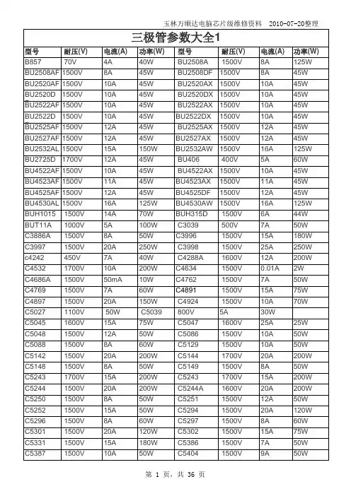
玉林万顺达电脑芯片级维修资料 2010-07-20整理玉林万顺达电脑芯片级维修资料 2010-07-20整理玉林万顺达电脑芯片级维修资料 2010-07-20整理玉林万顺达电脑芯片级维修资料 2010-07-20整理玉林万顺达电脑芯片级维修资料 2010-07-20整理玉林万顺达电脑芯片级维修资料 2010-07-20整理玉林万顺达电脑芯片级维修资料 2010-07-20整理玉林万顺达电脑芯片级维修资料 2010-07-20整理玉林万顺达电脑芯片级维修资料 2010-07-20整理玉林万顺达电脑芯片级维修资料 2010-07-20整理玉林万顺达电脑芯片级维修资料 2010-07-20整理玉林万顺达电脑芯片级维修资料 2010-07-20整理玉林万顺达电脑芯片级维修资料 2010-07-20整理玉林万顺达电脑芯片级维修资料 2010-07-20整理玉林万顺达电脑芯片级维修资料 2010-07-20整理玉林万顺达电脑芯片级维修资料 2010-07-20整理玉林万顺达电脑芯片级维修资料 2010-07-20整理玉林万顺达电脑芯片级维修资料 2010-07-20整理玉林万顺达电脑芯片级维修资料 2010-07-20整理玉林万顺达电脑芯片级维修资料 2010-07-20整理玉林万顺达电脑芯片级维修资料 2010-07-20整理玉林万顺达电脑芯片级维修资料 2010-07-20整理玉林万顺达电脑芯片级维修资料 2010-07-20整理玉林万顺达电脑芯片级维修资料 2010-07-20整理玉林万顺达电脑芯片级维修资料 2010-07-20整理玉林万顺达电脑芯片级维修资料 2010-07-20整理玉林万顺达电脑芯片级维修资料 2010-07-20整理玉林万顺达电脑芯片级维修资料 2010-07-20整理玉林万顺达电脑芯片级维修资料 2010-07-20整理玉林万顺达电脑芯片级维修资料 2010-07-20整理。
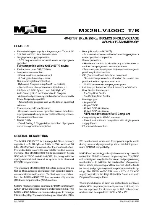
MX29LV400C T/B4M-BIT [512K x 8 / 256K x 16] CMOS SINGLE VOLTAGE3V ONLY FLASH MEMORY•Ready/Busy# pin (RY/BY#)- Provides a hardware method of detecting program or erase operation completion •Sector protection- Hardware method to disable any combination of sectors from program or erase operations- Temporary sector unprotect allows code changes in previously locked sectors•CFI (Common Flash Interface) compliant- Flash device parameters stored on the device and provide the host system to access•100,000 minimum erase/program cycles•Latch-up protected to 100mA from -1V to VCC+1V •Boot Sector Architecture - T = Top Boot Sector - B = Bottom Boot Sector •Package type:- 44-pin SOP - 48-pin TSOP- 48-ball CSP (6 x 8mm)- 48-ball CSP (4 x 6mm)- All Pb-free devices are RoHS Compliant •Compatibility with JEDEC standard- Pinout and software compatible with single-power supply Flash•20 years data retentionFEATURES•Extended single - supply voltage range 2.7V to 3.6V •524,288 x 8/262,144 x 16 switchable •Single power supply operation- 3.0V only operation for read, erase and program operation•Fully compatible with MX29LV400T/B device •Fast access time: 55R/70/90ns •Low power consumption- 30mA maximum active current - 0.2uA typical standby current •Command register architecture- Byte/word Programming (9us/11us typical)- Sector Erase (Sector structure 16K-Byte x 1,8K-Byte x 2, 32K-Byte x1, and 64K-Byte x7)•Auto Erase (chip & sector) and Auto Program- Automatically erase any combination of sectors with Erase Suspend capability- Automatically program and verify data at specified address•Erase suspend/Erase Resume- Suspends sector erase operation to read data from,or program data to, any sector that is not being erased,then resumes the erase •Status Reply- Data# Polling & Toggle bit for detection of program and erase operation completionGENERAL DESCRIPTIONThe MX29LV400C T/B is a 4-mega bit Flash memory organized as 512K bytes of 8 bits or 256K words of 16bits. MXIC's Flash memories offer the most cost-effec-tive and reliable read/write non-volatile random access memory. The MX29LV400C T/B is packaged in 44-pin SOP , 48-pin TSOP and 48-ball CSP . It is designed to be reprogrammed and erased in system or in standard EPROM programmers.The standard MX29LV400C T/B offers access time as fast as 55ns, allowing operation of high-speed micropro-cessors without wait states. To eliminate bus conten-tion, the MX29LV400C T/B has separate chip enable (CE#) and output enable (OE#) controls.MXIC's Flash memories augment EPROM functionality with in-circuit electrical erasure and programming. The MX29LV400C T/B uses a command register to manage this functionality. The command register allows for 100%TTL level control inputs and fixed power supply levels during erase and programming, while maintaining maxi-mum EPROM compatibility.MXIC Flash technology reliably stores memory contents even after 100,000 erase and program cycles. The MXIC cell is designed to optimize the erase and programming mechanisms. In addition, the combination of advanced tunnel oxide processing and low internal electric fields for erase and program operations produces reliable cy-cling. The MX29LV400C T/B uses a 2.7V~3.6V VCC supply to perform the High Reliability Erase and auto Program/Erase algorithms.The highest degree of latch-up protection is achieved with MXIC's proprietary non-epi process. Latch-up pro-tection is proved for stresses up to 100 milliamps on address and data pin from -1V to VCC + 1V .MX29LV400C T/BPIN CONFIGURATIONS 44 SOP(500 mil)PIN DESCRIPTIONSYMBOL PIN NAMEA0~A17Address InputQ0~Q14Data Input/OutputQ15/A-1Q15 (Word mode)/LSB addr(Byte mode) CE#Chip Enable InputWE#Write Enable InputBYTE#Word/Byte Selection inputRESET#Hardware Reset Pin/Sector ProtectUnlockOE#Output Enable InputRY/BY#Ready/Busy OutputVCC Power Supply Pin (2.7V~3.6V)GND Ground PinNC Pin Not Connected Internally48 TSOP (Standard Type) (12mm x 20mm)A15A14A13A12A11A10A9A8NCNCWE# RESET#NCNC RY/BY#NCA17A7A6A5A4A3A2A1123456789101112131415161718192021222324A16BYTE#GNDQ15/A-1Q7Q14Q6Q13Q5Q12Q4VCCQ11Q3Q10Q2Q9Q1Q8Q0OE#GNDCE#A0484746454443424140393837363534333231302928272625MX29LV400C T/B2 3 4 5 6 7 8 9 10 11 12 13 14 15 16 17 18 19 20 21 2244 43 42 41 40 39 38 37 36 35 34 33 32 31 30 29 28 27 26 25 24 23NC RY/BY#A17A7A6A5A4A3A2A1A0CE#GNDOE#Q0Q8Q1Q9Q2Q10Q3Q11RESET#WE#A8A9A10A11A12A13A14A15A16BYTE#GNDQ15/A-1Q7Q14Q6Q13Q5Q12Q4VCCMX29LV4CT/BMX29LV400C T/BMX29LV400C T/BBLOCK STRUCTURETable 1: MX29LV400CT SECTOR ARCHITECTURE Note: Byte mode:address range A17:A-1, word mode:address range A17:A0.Sector Sector SizeAddress range Sector AddressByte Mode Word ModeByte Mode (x8)Word Mode (x16)A17A16A15A14A13A12SA064Kbytes 32Kwords 00000-0FFFF 00000-07FFF 000X X X SA164Kbytes 32Kwords 10000-1FFFF 08000-0FFFF 001X X X SA264Kbytes 32Kwords 20000-2FFFF 10000-17FFF 010X X X SA364Kbytes 32Kwords 30000-3FFFF 18000-1FFFF 011X X X SA464Kbytes 32Kwords 40000-4FFFF 20000-27FFF 100X X X SA564Kbytes 32Kwords 50000-5FFFF 28000-2FFFF 101X X X SA664Kbytes 32Kwords 60000-6FFFF 30000-37FFF 110X X X SA732Kbytes 16Kwords 70000-77FFF 38000-3BFFF 1110X X SA88Kbytes 4Kwords 78000-79FFF 3C000-3CFFF 111100SA98Kbytes 4Kwords 7A000-7BFFF 3D000-3DFFF 111101SA1016Kbytes8Kwords7C000-7FFFF3E000-3FFFF11111XSector Sector SizeAddress range Sector AddressByte Mode Word ModeByte Mode (x8)Word Mode (x16)A17A16A15A14A13A12SA016Kbytes 8Kwords 00000-03FFF 00000-01FFF 00000X SA18Kbytes 4Kwords 04000-05FFF 02000-02FFF 000010SA28Kbytes 4Kwords 06000-07FFF 03000-03FFF 000011SA332Kbytes 16Kwords 08000-0FFFF 04000-07FFF 0001X X SA464Kbytes 32Kwords 10000-1FFFF 08000-0FFFF 001X X X SA564Kbytes 32Kwords 20000-2FFFF 10000-17FFF 010X X X SA664Kbytes 32Kwords 30000-3FFFF 18000-1FFFF 011X X X SA764Kbytes 32Kwords 40000-4FFFF 20000-27FFF 100X X X SA864Kbytes 32Kwords 50000-5FFFF 28000-2FFFF 101X X X SA964Kbytes 32Kwords 60000-6FFFF 30000-37FFF 110X X X SA1064Kbytes32Kwords70000-7FFFF38000-3FFFF111XXXTable 2: MX29LV400CB SECTOR ARCHITECTURE Note: Byte mode:address range A17:A-1, word mode:address range A17:A0.MX29LV400C T/BBLOCK DIAGRAMCONTROL INPUT LOGICPROGRAM/ERASE HIGH VOLTAGEWRITE STATE MACHINE (WSM)STATE REGISTERFLASH ARRAYX-DECODERADDRESS LATCHAND BUFFERY -PASS GATEY -DECODERARRAY SOURCE HVCOMMAND DATADECODERCOMMAND DATA LATCHI/O BUFFERPGM DATA HVPROGRAM DATA LATCHSENSE AMPLIFIERQ0-Q15/A-1A0-A17CE#OE#WE#RESET#MX29LV400C T/BAUTOMATIC PROGRAMMINGThe MX29L V400C T/B is byte programmable using the Automatic Programming algorithm. The Automatic Pro-gramming algorithm makes the external system do not need to have time out sequence nor to verify the data programmed. The typical chip programming time at room temperature of the MX29LV400C T/B is less than 10 seconds.AUTOMATIC CHIP ERASEThe entire chip is bulk erased using 10 ms erase pulses according to MXIC's Automatic Chip Erase algorithm. T ypical erasure at room temperature is accomplished in less than 4 second. The Automatic Erase algorithm au-tomatically programs the entire array prior to electrical erase. The timing and verification of electrical erase are controlled internally within the device.AUTOMATIC SECTOR ERASEThe MX29L V400C T/B is sector(s) erasable using MXIC's Auto Sector Erase algorithm. The Automatic Sector Erase algorithm automatically programs the specified sector(s) prior to electrical erase. The timing and verifi-cation of electrical erase are controlled internally within the device. An erase operation can erase one sector, multiple sectors, or the entire device.AUTOMATIC PROGRAMMING ALGORITHMMXIC's Automatic Programming algorithm requires the user to only write program set-up commands (including 2 unlock write cycle and A0H) and a program command (program data and address). The device automatically times the programming pulse width, provides the pro-gram verification, and counts the number of sequences.A status bit similar to Data# Polling and a status bit toggling between consecutive read cycles, provide feed-back to the user as to the status of the programming operation. Refer to write operation status, table7, for more information on these status bits.AUTOMATIC ERASE ALGORITHMMXIC's Automatic Erase algorithm requires the user to write commands to the command register using stan-dard microprocessor write timings. The device will auto-matically pre-program and verify the entire array. Then the device automatically times the erase pulse width, provides the erase verification, and counts the number of sequences. A status bit toggling between consecutive read cycles provides feedback to the user as to the sta-tus of the erasing operation.Register contents serve as inputs to an internal state-machine which controls the erase and programming cir-cuitry. During write cycles, the command register inter-nally latches address and data needed for the program-ming and erase operations. During a system write cycle, addresses are latched on the falling edge, and data are latched on the rising edge of WE# or CE#, whichever happens first.MXIC's Flash technology combines years of EPROM experience to produce the highest levels of quality, reli-ability, and cost effectiveness. The MX29LV400C T/B electrically erases all bits simultaneously using Fowler-Nordheim tunneling. The bytes are programmed by us-ing the EPROM programming mechanism of hot elec-tron injection.During a program cycle, the state-machine will control the program sequences and command register will not respond to any command set. During a Sector Erase cycle, the command register will only respond to Erase Suspend command. After Erase Suspend is completed, the device stays in read mode. After the state machine has completed its task, it will allow the command regis-ter to respond to its full command set.AUTOMATIC SELECTThe automatic select mode provides manufacturer and device identification, and sector protection verification, through identifier codes output on Q7~Q0. This mode is mainly adapted for programming equipment on the de-vice to be programmed with its programming algorithm. When programming by high voltage method, automatic select mode requires VID (11.5V to 12.5V) on address pin A9 and other address pin A6, A1 as referring to T able 3. In addition, to access the automatic select codes in-system, the host can issue the automatic select com-mand through the command register without requiring VID, as shown in table4.To verify whether or not sector being protected, the sec-tor address must appear on the appropriate highest orderMX29LV400C T/BTABLE 3. MX29LV400C T/B AUTO SELECT MODE OPERATIONNOTE:SA=Sector Address, X=Don't Care, L=Logic Low, H=Logic HighA17A11A8A5DescriptionMode CE#OE#WE#RE- | |A9 |A6 |A1A0Q15~Q0SET#A12A10A7A2Manufacture LLHHXX VID XLXLLC2HCodeRead Device ID Word L L H H X X VID X L X L H 22B9H Silicon (T op Boot Block)Byte L L H H X X VID X L X L H XXB9H IDDevice ID (Bottom Word L L H H X X VID X L X L H 22BAH Boot Block)ByteL L H H X X VID X L X L H XXBAH XX01H Sector Protection LLHHSAX VID XLXHL(protected)VerificationXX00H (unprotected)address bit (see T able 1 and T able 2). The rest of address bits, as shown in table3, are don't care. Once all neces-sary bits have been set as required, the programming equipment may read the corresponding identifier code on Q7~Q0.MX29LV400C T/BTABLE 4. MX29LV400C T/B COMMAND DEFINITIONSFirst Bus Second Bus Third Bus Fourth Bus Fifth Bus Sixth Bus Command Bus Cycle Cycle Cycle Cycle Cycle CycleCycle Addr Data Addr Data Addr Data Addr Data Addr Data Addr Data Reset 1XXXH F0HRead1RA RDRead Silicon ID Word4555H AAH2AAH55H555H90H ADI DDIByte4AAAH AAH555H55H AAAH90H ADI DDISector Protect Word4555H AAH2AAH55H555H90H(SA)XX00HVerify x02H XX01HByte4AAAH AAH555H55H AAAH90H(SA)00Hx04H01HProgram Word4555H AAH2AAH55H555H A0H PA PDByte4AAAH AAH555H55H AAAH A0H PA PDChip Erase Word6555H AAH2AAH55H555H80H555H AAH2AAH55H555H10H Byte6AAAH AAH555H55H AAAH80H AAAH AAH555H55H AAAH10H Sector Erase Word6555H AAH2AAH55H555H80H555H AAH2AAH55H SA30H Byte6AAAH AAH555H55H AAAH80H AAAH AAH555H55H SA30H Sector Erase Suspend1XXXH B0HSector Erase Resume1XXXH30HCFI Query Word155H98Byte1AAH98Note:1.ADI = Address of Device identifier; A1=0, A0 = 0 for manufacturer code,A1=0, A0 = 1 for device code. A2-A17=do not care.(Refer to table 3)DDI = Data of Device identifier : C2H for manufacture code, B9H/BAH (x8) and 22B9H/22BAH (x16) for device code.X = X can be VIL or VIHRA=Address of memory location to be read.RD=Data to be read at location RA.2.P A = Address of memory location to be programmed.PD = Data to be programmed at location P A.SA = Address of the sector to be erased.3.The system should generate the following address patterns: 555H or 2AAH to Address A10~A0 in word mode/AAAH or555H to Address A10~A-1 in byte mode.Address bit A11~A17=X=Don't care for all address commands except for Program Address (PA) and SectorAddress (SA). Write Sequence may be initiated with A11~A17 in either state.4.For Sector Protect Verify operation: If read out data is 01H, it means the sector has been protected. If read out data is 00H, itmeans the sector is still not being protected.5.Any number of CFI data read cycle are permitted.MX29LV400C T/BADDRESSQ8~Q15DESCRIPTIONCE#OE#WE#RE- A17A10A9A8A6A5A1A0Q0~Q7BYTE BYTE SET#A11A7A2=VIH=VILReadLLHHAINDoutDout Q8~Q14=High ZQ15=A-1Write L H L H AIN DIN(3)DIN Q8~Q14=High ZQ15=A-1ResetX X X L X High Z High Z High Z Temporary sector unlock X X X VID AIN DIN DIN High Z Output Disable L H H H X High Z High Z High Z StandbyVcc ±XXVcc ±XHigh ZHigh ZHigh Z0.3V0.3VSector Protect L H L VID SA X X X L X H L DIN X X Chip Unprotect L H L VID X XXXH X H L DIN X X Sector Protection VerifyLLHHSAX VID XLXHLCODE(5)XXTABLE 5. MX29L V400C T/B BUS OPERATIONNOTES:1. Manufacturer and device codes may also be accessed via a command register write sequence. Refer to T able 4.2. VID is the Silicon-ID-Read high voltage, 11.5V to 12.5V .3. Refer to T able 4 for valid Data-In during a write operation.4. X can be VIL or VIH.5. Code=00H/XX00H means unprotected.Code=01H/XX01H means protected.6.A17~A12=Sector address for sector protect.7.The sector protect and chip unprotect functions may also be implemented via programming equipment.sequences. Note that the Erase Suspend (B0H) and Erase Resume (30H) commands are valid only while the Sector Erase operation is in progress.COMMAND DEFINITIONSDevice operations are selected by writing specific ad-dress and data sequences into the command register.Writing incorrect address and data values or writing them in the improper sequence will reset the device to the read mode. Table 4 defines the valid register commandMX29LV400C T/BREQUIREMENTS FOR READING ARRAY DATATo read array data from the outputs, the system must drive the CE# and OE# pins to VIL. CE# is the power control and selects the device. OE# is the output control and gates array data to the output pins. WE# should re-main at VIH.The internal state machine is set for reading array data upon device power-up, or after a hardware reset. This ensures that no spurious alteration of the memory con-tent occurs during the power transition. No command is necessary in this mode to obtain array data. Standard microprocessor read cycles that assert valid address on the device address inputs produce valid data on the de-vice data outputs. The device remains enabled for read access until the command register contents are altered. WRITE COMMANDS/COMMAND SEQUENCEST o program data to the device or erase sectors of memory , the system must drive WE# and CE# to VIL, and OE# to VIH.An erase operation can erase one sector, multiple sec-tors , or the entire device. Table indicates the address space that each sector occupies. A "sector address" consists of the address bits required to uniquely select a sector. The "Writing specific address and data commands or sequences into the command register initiates device operations. Table 1 defines the valid register command sequences. Writing incorrect address and data values or writing them in the improper sequence resets the device to reading array data. Section has details on erasing a sector or the entire chip, or suspending/resuming the erase operation.After the system writes the autoselect command se-quence, the device enters the autoselect mode. The sys-tem can then read autoselect codes from the internal reg-ister (which is separate from the memory array) on Q7-Q0. Standard read cycle timings apply in this mode. Re-fer to the Autoselect Mode and Autoselect Command Sequence section for more information.ICC2 in the DC Characteristics table represents the ac-tive current specification for the write mode. The "AC Characteristics" section contains timing specification table and timing diagrams for write operations.STANDBY MODEWhen using both pins of CE# and RESET#, the device enter CMOS Standby with both pins held at Vcc ± 0.3V. If CE# and RESET# are held at VIH, but not within the range of VCC ± 0.3V, the device will still be in the standby mode, but the standby current will be larger. During Auto Algorithm operation, Vcc active current (Icc2) is required even CE# = "H" until the operation is completed. The device can be read with standard access time (tCE) from either of these standby modes, before it is ready to read data.OUTPUT DISABLEWith the OE# input at a logic high level (VIH), output from the devices are disabled. This will cause the output pins to be in a high impedance state.RESET# OPERATIONThe RESET# pin provides a hardware method of reset-ting the device to reading array data. When the RESET# pin is driven low for at least a period of tRP, the device immediately terminates any operation in progress, tristates all output pins, and ignores all read/write com-mands for the duration of the RESET# pulse. The device also resets the internal state machine to reading array data. The operation that was interrupted should be reinitiated once the device is ready to accept another command sequence, to ensure data integrityCurrent is reduced for the duration of the RESET# pulse. When RESET# is held at VSS±0.3V, the device draws CMOS standby current (ICC4). If RESET# is held at VIL but not within VSS±0.3V, the standby current will be greater.The RESET# pin may be tied to system reset circuitry.A system reset would that also reset the Flash memory, enabling the system to read the boot-up firm-ware from the Flash memory.If RESET# is asserted during a program or erase opera-tion, the RY/BY# pin remains a "0" (busy) until the inter-nal reset operation is complete, which requires a time of tREADY (during Embedded Algorithms). The system can thus monitor RY/BY# to determine whether the reset op-eration is complete. If RESET# is asserted when a pro-MX29LV400C T/Bgram or erase operation is completed within a time of tREADY (not during Embedded Algorithms). The system can read data tRH after the RESET# pin returns to VIH. Refer to the AC Characteristics tables for RESET# pa-rameters and to Figure 24 for the timing diagram.READ/RESET COMMANDThe read or reset operation is initiated by writing the read/ reset command sequence into the command register. Microprocessor read cycles retrieve array data. The de-vice remains enabled for reads until the command regis-ter contents are altered.If program-fail or erase-fail happen, the write of F0H will reset the device to abort the operation. A valid com-mand must then be written to place the device in the desired state.SILICON-ID READ COMMANDFlash memories are intended for use in applications where the local CPU alters memory contents. As such, manu-facturer and device codes must be accessible while the device resides in the target system. PROM program-mers typically access signature codes by raising A9 to a high voltage (VID). However, multiplexing high voltage onto address lines is not generally desired system de-sign practice.The MX29LV400C T/B contains a Silicon-ID-Read op-eration to supple traditional PROM programming meth-odology. The operation is initiated by writing the read silicon ID command sequence into the command regis-ter. Following the command write, a read cycle with A1=VIL, A0=VIL retrieves the manufacturer code of C2H/ 00C2H. A read cycle with A1=VIL, A0=VIH returns the device code of B9H/22B9H for MX29LV400CT, BAH/ 22BAH for MX29LV400CB.SET-UP AUTOMATIC CHIP/SECTOR ERASE COM-MANDSChip erase is a six-bus cycle operation. There are two "unlock" write cycles. These are followed by writing the "set-up" command 80H. T wo more "unlock" write cycles are then followed by the chip erase command 10H or sector erase command 30H.The Automatic Chip Erase does not require the device to be entirely pre-programmed prior to executing the Auto-matic Chip Erase. Upon executing the Automatic Chip Erase, the device will automatically program and verify the entire memory for an all-zero data pattern. When the device is automatically verified to contain an all-zero pat-tern, a self-timed chip erase and verify begin. The erase and verify operations are completed when the data on Q7 is "1" at which time the device returns to the Read mode. The system is not required to provide any control or timing during these operations.When using the Automatic Chip Erase algorithm, note that the erase automatically terminates when adequate erase margin has been achieved for the memory array (no erase verification command is required).If the Erase operation was unsuccessful, the data on Q5 is "1"(see Table 7), indicating the erase operation ex-ceed internal timing limit.The automatic erase begins on the rising edge of the last WE# or CE# pulse, whichever happens first in the com-mand sequence and terminates when the data on Q7 is "1" at which time the device returns to the Read mode, or the data on Q6 stops toggling for two consecutive read cycles at which time the device returns to the Read mode.MX29LV400C T/BPins A0A1Q15~Q8Q7Q6Q5Q4Q3Q2Q1Q0Code(Hex)Manufacture code Word VIL VIL00H1100001000C2HByte VIL VIL X11000010C2H Device code Word VIH VIL22H1011100122B9Hfor MX29LV400CT Byte VIH VIL X10111001B9HDevice code Word VIH VIL22H1011101022BAHfor MX29LV400CB Byte VIH VIL X10111010BAHSector Protection X VIH X0000000101H (Protected) Verification X VIH X0000000000H (Unprotected) TABLE 6. EXPANDED SILICON ID CODEREADING ARRA Y DATAThe device is automatically set to reading array data after device power-up. No commands are required to re-trieve data. The device is also ready to read array data after completing an Automatic Program or Automatic Erase algorithm.After the device accepts an Erase Suspend command, the device enters the Erase Suspend mode. The sys-tem can read array data using the standard read tim-ings, except that if it reads at an address within erase-suspended sectors, the device outputs status data. Af-ter completing a programming operation in the Erase Suspend mode, the system may once again read array data with the same exception. See "Erase Suspend/Erase Resume Commands" for more infor-mation on this mode. The system must issue the reset command to re-en-able the device for reading array data if Q5 goes high, or while in the autoselect mode. See the "Reset Command" section, next.RESET COMMANDWriting the reset command to the device resets the de-vice to reading array data. Address bits are don't care for this command.The reset command may be written between the se-quence cycles in an erase command sequence before erasing begins. This resets the device to reading array data. Once erasure begins, however, the device ignores reset commands until the operation is complete.The reset command may be written between the se-quence cycles in a program command sequence be-fore programming begins. This resets the device to reading array data (also applies to programming in Erase Sus-pend mode). Once programming begins, however, the device ignores reset commands until the operation is complete.The reset command may be written between the se-quence cycles in an SILICON ID READ command se-quence. Once in the SILICON ID READ mode, the reset command must be written to return to reading array data (also applies to SILICON ID READ during Erase Sus-pend).If Q5 goes high during a program or erase operation, writ-ing the reset command returns the device to read-ing array data (also applies during Erase Suspend).MX29LV400C T/Berase margin has been achieved for the memory array (no erase verification command is required). Sector erase is a six-bus cycle operation. There are two "un-lock" write cycles. These are followed by writing the set-up command 80H. Two more "unlock" write cycles are then followed by the sector erase command 30H. The sector address is latched on the falling edge of WE# or CE#, whichever happens later, while the command (data)is latched on the rising edge of WE# or CE#, whichever happens first. Sector addresses selected are loaded into internal register on the sixth falling edge of WE# or CE#, whichever happens later. Each successive sector load cycle started by the falling edge of WE# or CE#,whichever happens later must begin within 50us from the rising edge of the preceding WE# or CE#, whichever happens first. Otherwise, the loading period ends and internal auto sector erase cycle starts. (Monitor Q3 to determine if the sector erase timer window is still open,see section Q3, Sector Erase Timer.) Any command other than Sector Erase(30H) or Erase Suspend(B0H) during the time-out period resets the device to read mode.SECTOR ERASE COMMANDSThe Automatic Sector Erase does not require the de-vice to be entirely pre-programmed prior to executing the Automatic Sector Erase Set-up command and Au-tomatic Sector Erase command. Upon executing the Automatic Sector Erase command, the device will auto-matically program and verify the sector(s) memory for an all-zero data pattern. The system is not required to provide any control or timing during these operations.When the sector(s) is automatically verified to contain an all-zero pattern, a self-timed sector erase and verify begin. The erase and verify operations are complete when either the data on Q7 is "1" at which time the de-vice returns to the Read mode, or the data on Q6 stops toggling for two consecutive read cycles at which time the device returns to the Read mode. The system is not required to provide any control or timing during these operations.When using the Automatic sector Erase algorithm, note that the erase automatically terminates when adequateStatusQ7Q6Q5Q3Q2RY/(Note1)(Note2)BY#Byte Program in Auto Program Algorithm Q7#Toggle 0N/A No 0Toggle Auto Erase Algorithm0Toggle 01Toggle0Erase Suspend Read1No 0N/A Toggle1(Erase Suspended Sector)Toggle In ProgressErase Suspended ModeErase Suspend ReadData Data Data Data Data 1(Non-Erase Suspended Sector)Erase Suspend ProgramQ7#Toggle 0N/A N/A 0Byte Program in Auto Program AlgorithmQ7#Toggle 1N/A No 0Toggle ExceededTime Limits Auto Erase Algorithm0Toggle 11Toggle 0Erase Suspend ProgramQ7#Toggle1N/AN/ATable 7. Write Operation StatusNote:1.Q7 and Q2 require a valid address when reading status information. Refer to the appropriate subsection for further details.2.Q5 switches to '1' when an Auto Program or Auto Erase operation has exceeded the maximum timing limits.See "Q5:Exceeded Timing Limits " for more information.。
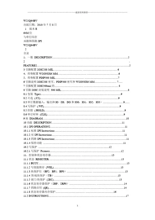
W25Q64BV出版日期:2010年7月8日- 1 - 版本E64M位与串行闪存双路和四路SPIW25Q64BV- 2 -目录1,一般DESCRIPTION (5)2。
FEATURES (5)3引脚配置SOIC208-MIL.......................................... .. (6)4,焊垫配置WSON8X6-MM.......................................... . (6)5,焊垫配置PDIP300-MIL.......................................... . (7)6引脚说明SOIC208密耳,PDIP300密耳和WSON8X6-MM................................ 7......7引脚配置SOIC300mil的.......................................... .. (8)8引脚SOIC封装说明300-MIL (8)8.1包装Types (9)8.2片选(/CS) (9)8.3串行数据输入,输出和IO(DI,DO和IO0,IO1,IO2,IO3)............................. 9.......8.4写保护(/WP) (9)8.5控股(/HOLD) (9)8.6串行时钟(CLK) (9)9座DIAGRAM (10)10功能DESCRIPTION (11)10.1 SPI OPERATIONS (11)10.1.1标准SPI Instructions (11)10.1.2双SPI Instructions (11)10.1.3四路SPI Instructions (11)10.1.4保持功能 (11)10.2写保护 (12)10.2.1写保护Features (12)11,控制和状态寄存器............................................ .. (13)11.1状态REGISTER (13)11.1.1 BUSY (13)11.1.2写使能锁存(WEL) (13)11.1.3块保护位(BP2,BP1,BP0)..................................... .. (13)11.1.4顶/底块保护(TB)....................................... .................................................. ..1311.1.5部门/块保护(SEC) (13)11.1.6状态寄存器保护(SRP,SRP0)....................................... . (14)11.1.7四路启用(QE) (14)11.1.8状态寄存器内存保护........................................... .. (16)11.2 INSTRUCTIONS (17)11.2.1制造商和设备标识........................................... .. (17)11.2.2指令集表1 (18)W25Q64BV11.2.3指令表2(阅读说明书)....................................... (19)出版日期:2010年7月8日- 3 - 修订版E11.2.4写使能(06h) (20)11.2.5写禁止(04h) (20)11.2.6读状态寄存器1(05H)和读状态寄存器2(35H).............................. (21)11.2.7写状态寄存器(01H)......................................... .................................................. .. (22)11.2.8读取数据(03h) (23)11.2.9快速阅读(0Bh) (24)11.2.10快速读双输出(3BH)........................................ .................................................. 0.25 11.2.11快速读四路输出(6BH)........................................ .. (26)11.2.12快速读双I / O (BBh) (27)11.2.13快速读取四I/ O (EBh) (29)11.2.14八进制字读取四I/ O(E3H)..................................... (31)11.2.15页编程(02h) (33)11.2.16四路输入页编程(32H)........................................ . (34)11.2.17扇区擦除(20H) (35)11.2.1832KB的块擦除(52H) (36)11.2.1964KB的块擦除(D8h) (37)20年2月11日芯片擦除(C7H/ 60h) (38)21年2月11日擦除挂起(75h) (39)22年2月11日擦除恢复(7Ah) (40)23年11月2日掉电(B9h) (41)24年2月11日高性能模式(A3H)......................................... (42)25年2月11日发布掉电或高性能模式/设备ID(ABH) (42)26年2月11日读制造商/设备ID(90H)....................................... . (44)27年2月11日阅读唯一的ID号(4BH)........................................ . (45)28年2月11日读JEDEC的ID (9Fh) (46)29年2月11日连续读取模式复位(FFH或FFFFH)...................................... .. (47)12,电气特性.............................................. (48)12.1绝对最大Ratings (48)12.2操作范围 (48)12.3上电时序和写抑制阈值......................................... (49)12.4直流电气Characteristics (50)12.5 AC测量条件.............................................. .. (51)12.6 AC电气Characteristics (52)12.7 AC电气特性(续)......................................... . (53)12.8串行输出Timing (54)12.9输入Timing (54)12.10持有Timing (54)13包装SPECIFICATION (55)W25Q64BV13.18引脚SOIC208密耳(包装代号SS)..................................... .. (55)- 4 -13.28引脚PDIP300密耳(封装代码DA)..................................... (56)13.38触点WSON8x6毫米(封装代码ZE)....................................... (57)13.416引脚SOIC300密耳(封装代码SF)..................................... . (58)14订货INFORMA TION (59)14.1有效的部件号和顶端标记.......................................... (60)15版本HISTORY (61)W25Q64BV出版日期:2010年7月8日- 5 - 修订版E1概述该W25Q64BV(64M位)串行Flash存储器提供了有限的系统存储解决方案空间,引脚和电源。

EW-7317UHg802.11b/g 6dBi高功率指向性USB無線網路卡中文使用手冊Version: 1.1 (August, 2007)警告聲明本設備已通過測試並符合 FCC 規則第 15 部分有關數位裝置的規定。
這些限制的主要目的是在保護商業區中運作此種設備時,提供合理程度的保護,避免有害干擾。
本設備會產生、使用並放射射頻能源,若不按指示手冊安裝和使用,會對無線通訊造成有害干擾。
在住宅區中運作本設備亦可能造成有害干擾,在這種情況下,使用者會被要求採用以下一種或多種方法來改善干擾的情形:1. 調整接收天線的方向或移動其位置。
2. 將設備與接收天線的距離增加。
3. 諮詢經銷商或有經驗的無線電/電視技術員的協助。
FCC 聲明這個設備遵照FCC 規則第15節,操作程序受限於以下二個條件:(1) 這個設備不能導致有害的干擾。
(2) 這個設備必須可接受任一種干擾,包括可能導致非預期操作的干擾。
FCC輻射暴露聲明:本設備完全符合美國聯邦通訊委員會針對非控制環境所提出之輻射暴露限制。
用戶必須遵照所有滿足射頻暴露符合性之特殊操作說明,在正常操作時並距離該機器20公分以上。
本發射器所使用之天線在同一地點不得存在有其他天線或發射器或是與之合併操作。
CE標誌警告:本機器屬於Class B產品,適用於家用環境中,由於本產品可能會產生無線電干擾,因此用戶需採取適當防範措施。
R&TTE 符合性聲明本設備遵照2000年4月8日開始生效的1999/5/EC歐洲經濟共同體針對電信終端設備和衛星地面電臺設備之整合及互相承認(R&TTE) 所決議的所有要求。
安全性本設備之設計已針對安裝和使用上的安全性施以最大重視。
然而, 仍需對電擊和靜電的危險給予特別留意。
歐洲地區 EU Countries Intended for Use本機器的ETSI版本可以用於下列國家,澳洲、比利時、丹麥、芬蘭、法國、德國、希臘、愛爾蘭、義大利、盧森堡、荷蘭、西班牙、葡萄牙、瑞典及聯合王國之家庭及一般辦公室內。