HT1622
- 格式:pdf
- 大小:151.27 KB
- 文档页数:17
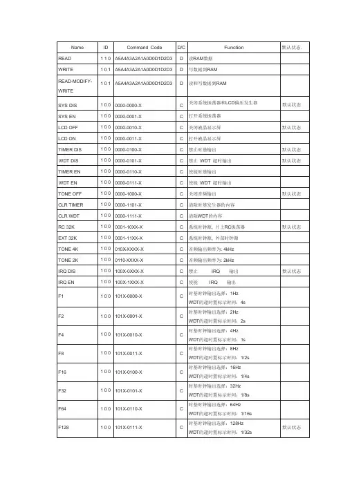
HT16270RAM Mapping 64´16LCD Controller for I/O m CSelection TableHT162X HT1620HT1621HT1622HT16220HT1623HT1625HT1626HT1627HT16270COM 448888161616SEG323232324864486464Built-in Osc.ÖÖÖÖÖÖCrystal Osc.ÖÖÖÖÖÖÖ1April 21,2000Features·Operating voltage:2.7V~5.2V·External Crystal 32.768kHz oscillator·1/5bias,1/16duty,frame frequency is 64Hz ·Max.64´16patterns,16commons,64segments·Built-in internal resistor type bias generator ·3-wire serial interface·8kinds of time base/WDT selection ·Time base or WDT overflow output ·Built-in LCD display RAM·R/W address auto increment·Two selectable buzzer frequencies (2kHz/4kHz)·Power down command reduces power consumption·Software configuration feature·Data mode and Command mode instructions ·Three data accessing modes·VLCD pin to adjust LCD operating voltageGeneral DescriptionHT16270is a peripheral device specially de-signed for I/O type m C used to expand the dis-play capability.The max.display segment of the device are 1024patterns (64´16).It also supports serial interface,buzzer sound,watch-dog timer or time base timer functions.The HT16270is a memory mapping and multi-function LCD controller.The softwareconfiguration feature of the HT16270make it suitable for multiple LCD applications includ-ing LCD modules and display subsystems.Only threelines are required for the interface be-tween the host controller and the HT16270.The HT162X series have many kinds of prod-ucts that match various applications.Block DiagramPin AssignmentHT162702April 21,2000Pad AssignmentChip size:245´237(mil)2*The IC substrate should be connected to VDD in the PCB layout artwork.HT162703April 21,2000Pad CoordinatesUnit:milPad No.X Y Pad No.X Y 1-116.5799.9049116.15-99.792-116.6890.8050116.15-93.163-116.7284.1551116.19-81.184-116.7277.5052116.19-74.545-116.7270.9053116.15-62.586-115.9364.2554116.19-55.937-116.7254.7555116.19-43.948-116.7241.4556116.19-37.409-116.7221.8557116.19-25.3710-115.9411.3958116.19-18.7011-115.94-0.6059116.19-6.7212-115.94-7.1860116.24-0.0913-115.90-19.2161116.2411.9014-115.97-25.8562116.1918.4915-115.93-37.8563116.2430.5116-115.93-44.4564116.1937.1017-115.93-56.4565116.1949.0918-115.93-63.0566116.1555.7619-115.97-75.0567116.1567.7520-115.93-81.7068116.1974.3821-115.93-93.6569116.1586.3622-115.94-100.3070116.1993.0323-115.94-112.3771116.11104.8524-108.08-112.0772112.20112.2425-96.03-112.0573100.04112.2426-89.43-112.057493.42112.2427-77.43-112.057581.43112.2428-70.82-112.057674.80112.2429-58.83-112.057762.77112.2430-52.17-112.057856.23112.2431-40.22-112.057944.20112.2432-33.58-112.058037.57112.2433-21.58-112.008125.63112.2434-14.98-112.058218.95112.2435-2.97-112.0083 6.97112.2436 3.67-112.05840.38112.243715.63-112.0585-11.65112.243822.27-112.0586-18.23112.203934.28-112.0587-30.22112.244040.88-112.0588-36.89112.244152.88-112.0589-48.92112.244259.47-112.0590-55.51112.244371.47-112.0091-67.45112.294478.13-112.0092-74.12112.244590.07-112.0593-86.15112.244696.72-112.0594-92.72112.2547108.72-112.0095-104.72112.2548116.19-111.8296-114.22112.25HT162704April 21,2000Pad DescriptionPad No.Pad Name I/O Description1DATA I/O Serial data input/output with pull-high resistor2VSS¾Negative power supply,ground3OSCI I Crystal oscillator input pin4OSCO O Crystal oscillato output pin5VDD¾Positive power supply6VLCD I LCD operating voltage input pad.7IRQ O Time base or watchdog timer overflow flag,NMOS open drainoutput8,9BZ,BZ O2kHz or4kHz tone frequency output pair(Tristate outputbuffer)10~13T1~T4I Not connected14~29COM0~COM15O LCD common outputs30~93SEG0~SEG63O LCD segment outputs94CS I Chip selection input with pull-high resistor.When the CS is logic high,the data and command read from or write to the HT16270are disabled.The serial interface circuit is also reset. But if the CS is at logic low level and is input to the CS pad,the data and command transmission between the host controller and the HT16270are all enabled.95RD I READ clock input with pull-high resistor.Data in the RAM of the HT16270are clocked out on the rising edge of the RD sig-nal.The clocked out data will appear on the data line.The host controller can use the next falling edge to latch the clocked out data.96WR I WRITE clock input with pull-high resistor.Data on the DATA line are latched into the HT16270on the rising edge of the WR signal.Absolute Maximum RatingsSupply Voltage.............................-0.3V to5.5V Storage Temperature.................-50°C to125°C Input Voltage.................V SS-0.3V to V DD+0.3V Operating Temperature..............-25°C to75°CNote:These are stress ratings only.Stresses exceeding the range specified under²Absolute Maxi-mum Ratings²may cause substantial damage to the device.Functional operation of this device at other conditions beyond those listed in the specification is not implied and prolonged expo-sure to extreme conditions may affect device reliability.5April21,2000Symbol Parameter Min.Typ.Max.UnitV DD ConditionsV DD Operating Voltage¾¾ 2.7¾ 5.2VI DD1Operating Current 3V No load/LCD ONCrystal oscillator¾3075m A 5V¾50125m AI DD2Operating Current 3V No load/LCD OFFCrystal oscillator¾525m A 5V¾1045m AI STB Standby Current 3V No loadPower down mode¾214m A 5V¾428m AV IL Input Low Voltage 3VDATA,WR,CS,RD0¾0.6V 5V0¾ 1.0VV IH Input High Voltage 3VDATA,WR,CS,RD2.4¾3V 5V 4.0¾5VI OL1BZ,BZ,IRQ 3V V OL=0.3V0.9 1.8¾mA 5V V OL=0.5V 1.73¾mAI OH1BZ,BZ 3V V OH=2.7V-0.9-1.8¾mA 5V V OH=4.5V-1.7-3¾mAI OL2DATA 3V V OL=0.3V0.9 1.8¾mA 5V V OL=0.5V 1.73¾mAI OH2DATA 3V V OH=2.7V-0.9-1.8¾mA 5V V OH=4.5V-1.7-3¾mAI OL3LCD Common Sink Current 3V V OL=0.3V80160¾m A 5V V OL=0.5V180360¾m AI OH3LCD Common Source Current 3V V OH=2.7V-40-80¾m A 5V V OH=4.5V-90-180¾m AI OL4LCD Segment Sink Current 3V V OL=0.3V50100¾m A 5V V OL=0.5V120240¾m AI OH4LCD Segment Source Current 3V V OH=2.7V-30-60¾m A 5V V OH=4.5V-70-140¾m AR PH Pull-high Resistor 3VDATA,WR,CS,RD100200300k W 5V50100150k W6April21,2000Symbol Parameter Min.Typ.Max.UnitV DD Conditionsf SYS System Clock 3VCrystal oscillator¾32¾kHz 5V¾32¾kHzf LCD LCD Frame Frequency 3VCrystal oscillator¾64¾Hz 5V¾64¾Hzt COM LCD Common Period¾n:Number of COM¾n/f LCD¾secf CLK1Serial Data Clock(WR Pin)3VDuty cycle50%¾¾150kHz 5V¾¾300kHzf CLK2Serial Data Clock(RD Pin)3VDuty cycle50%¾¾75kHz 5V¾¾150kHzt CS Serial Interface Reset PulseWidth(Figure3)¾CS¾250¾nst CLK WR,RD Input Pulse Width(Figure1)3VWrite mode 3.34¾¾m s Read mode 6.67¾¾5VWrite mode 1.67¾¾m s Read mode 3.34¾¾t r,t f Rise/Fall Time Serial Data Clock Width(Figure1)3V¾¾120¾ns 5Vt su Setup Time for DATA to WR,RD Clock Width(Figure2)3V¾¾120¾ns 5Vt h Hold Time for DATA to WR,RD Clock Width(Figure2)3V¾¾120¾ns 5Vt su1Setup Time for CS to WR,RDClock Width(Figure3)3V¾¾100¾ns 5Vt h1Hold Time for CS to WR,RDClock Width(Figure3)3V¾¾100¾ns 5V7April21,2000Figure1Figure2Figure3Functional DescriptionDisplay memory-RAM structureThe static display RAM is organized into256´4 bits and stores the display data.The contents of the RAM are directly mapped to the contents of the LCD driver.Data in the RAM can be a c c e s s e d b y t h e R E A D,W R I T E a n d READ-MODIFY-WRITE commands.The fol-lowing is a mapping from the RAM to the LCD patterns.Time base and watchdog timer-WDTThe time base generator and WDT share the same divided(/256)counter.TIMER DIS/EN/CLR, WDT DIS/EN/CLR and IRQ EN/DIS are inde-pendent from each other.Once the WDT time-out occurs,the IRQ pin will remain at logic low level until the CLR WDT or the IRQ DIS command is issued.RAM mapping8April21,20009April 21,2000Timer and WDT configurationsName Command Code FunctionTONE OFF 0000-1000-X Turn-off tone outputTONE 4K 010X-XXXX-X Turn-on tone output,tone frequency is 4kHz TONE 2K0110-XXXX-XTurn-on tone output,tone frequency is 2kHzIf an external clock is selected as the source of system frequency,the SYS DIS command turns out invalid and the power down mode fails to be carried out until the external clock source is re-moved.Buzzer tone outputA simple tone generator is implemented in the HT16270.The tone generator can output a pair of differential driving signals on the BZ and BZ which are used to generate a single mand formatThe HT16270can be configured by the software setting.There are two mode commands to con-figure the HT16270resource and to transfer the LCD display data.The following are the data mode ID and the command mode ID:OperationMode ID READ Data 110WRITEData 101READ-MODIFY-WRITE Data101COMMANDCommand 100If successive commands have been issued,the command mode ID can be omitted.While the system is operating in the non-successive com-mand or the non-successive address data mode,the CS pin should be set to ²1²and the previous operation mode will be reset also.The CS pin returns to ²0²,a new operation mode ID should be issued first.Timing DiagramsREAD mode(command code:110)READ mode(successive address reading)10April21,2000WRITE mode(command code:101)WRITE mode(successive address writing)11April21,2000READ-MODIFY-WRITE mode(command code:101)READ-MODIFY-WRITE mode(successive address accessing)12April21,2000Command mode(command code:100)Mode(data and command mode)13April21,2000Application Circuits*Note:The connection of IRQ and RD pin can be selected depending on the requirement of the m C.The voltage applied to V LCD pin must be lower than V DD.Adjust VR to fit LCD display,at V DD=5V,V LCD=4V,VR=15k W±20%.Adjust R(external pull-high resistance)to fit user¢s time base clock.14April21,2000Command SummaryName ID Command Code D/C Function Def. READ110A7A6A5A4A3A2A1A0D0D1D2D3D Read data from the RAMWRITE101A7A6A5A4A3A2A1A0D0D1D2D3D Write data to the RAMREAD-MODIFY-101A7A6A5A4A3A2A1A0D0D1D2D3D Read and Write data to the RAM WRITESYS DIS1000000-0000-X C Turn off both system oscillatorand LCD bias generator Yes SYS EN1000000-0001-X C Turn on system oscillatorLCD OFF1000000-0010-X C Turn off LCD display Yes LCD ON1000000-0011-X C Turn on LCD displayTIMER DIS1000000-0100-X C Disable time base output Yes WDT DIS1000000-0101-X C Disable WDT time-out flag output Yes TIMER EN1000000-0110-X C Enable time base outputWDT EN1000000-0111-X C Enable WDT time-out flag output TONE OFF1000000-1000-X C Turn off tone outputs YesCLR TIMER1000000-1101-X C Clear the contents of the time basegeneratorCLR WDT1000000-1111-X C Clear the contents of the WDT stage TONE4K100010X-XXXX-X C Tone frequency output:4kHzTONE2K1000110-XXXX-X C Tone frequency output:2kHzIRQ DIS100100X-0XXX-X C Disable IRQ output Yes IRQ EN100100X-1XXX-X C Enable IRQ outputF1100101X-0000-X C Time base clock output:1HzThe WDT time-out flag after:4sF2100101X-0001-X C Time base clock output:2HzThe WDT time-out flag after:2sF4100101X-0010-X C Time base clock output:4HzThe WDT time-out flag after:1sF8100101X-0011-X C Time base clock output:8HzThe WDT time-out flag after:1/2sF16100101X-0100-X C Time base clock output:16HzThe WDT time-out flag after:1/4s15April21,2000Name ID Command Code D/C Function Def. F32100101X-0101-X C Time base clock output:32HzThe WDT time-out flag after:1/8sF64100101X-0110-X C Time base clock output:64HzThe WDT time-out flag after:1/16sF128100101X-0111-X C Time base clock output:128HzThe WDT time-out flag after:1/32s Yes TEST1001110-0000-X C Test mode,user don¢t use.NORMAL1001110-0011-X C Normal mode Yes Note:X:Don¢t careA7~A0:RAM addressD3~D0:RAM dataD/C:Data/Command modeDef.:Power on reset defaultAll the bold forms,namely110,101,and100,are mode commands.Of these,100indicates the command mode ID.If successive commands have been issued,the command mode ID except for the first command will be omitted.The source of the tone frequency and of the time base/WDT clock fre-quency can be derived from a32.768kHz crystal oscillator or an external32kHz clock.Calculation of the frequency is based on the system frequency sources as stated above.It is recommended that the host controller should initialize the HT16270after power on reset,for power on reset may fail,which in turn leads to malfunctioning of the HT16270.16April21,200017April 21,2000Copyright Ó2000by HOLTEK SEMICONDUCTOR INC.The information appearing in this Data Sheet is believed to be accurate at the time of publication.However,Holtek assumes no responsibility arising from the use of the specifications described.The applications mentioned herein are used solely for the purpose of illustration and Holtek makes no warranty or representation that such applications will be suitable without further modification,nor recommends the use of its products for application that may pres-ent a risk to human life due to malfunction or otherwise.Holtek reserves the right to alter its products without prior notification.For the most up-to-date information,please visit our web site at .Holtek Semiconductor Inc.(Headquarters)No.3Creation Rd.II,Science-based Industrial Park,Hsinchu,Taiwan,R.O.C.Tel:886-3-563-1999Fax:886-3-563-1189Holtek Semiconductor Inc.(Taipei Office)5F,No.576,Sec.7Chung Hsiao E.Rd.,Taipei,Taiwan,R.O.C.Tel:886-2-2782-9635Fax:886-2-2782-9636Fax:886-2-2782-7128(International sales hotline)Holtek Semiconductor (Hong Kong)Ltd.RM.711,Tower 2,Cheung Sha Wan Plaza,833Cheung Sha Wan Rd.,Kowloon,Hong Kong Tel:852-2-745-8288Fax:852-2-742-8657。