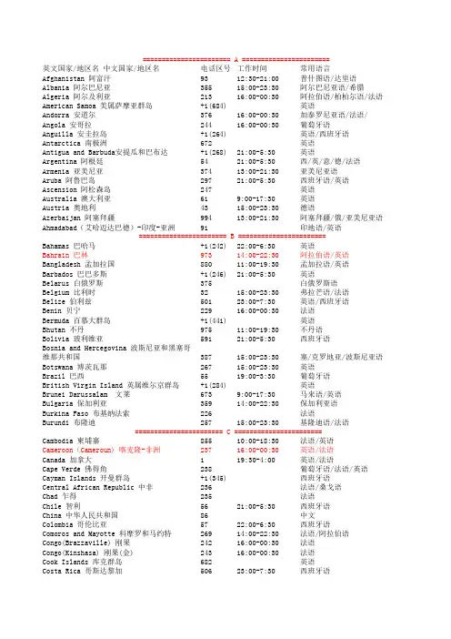
G961中文资料
- 格式:pdf
- 大小:234.58 KB
- 文档页数:6
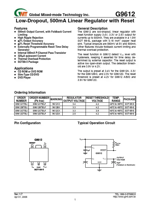
1A Low Dropout Regulator with EnableFeaturesAdjustable Output from 1.2V to 4.8V Using Ex-ternal Resistors1.5V, 1.8V and2.5V Options by Setting ADJ Pin Below 0.2VOver current and over temperature protection 400mV dropout @1A Enable pin10µA quiescent current in shutdownSOT-89-5 PackageApplicationsBattery powered systems Motherboards Peripheral cards Network cards Set Top Boxes Medical Equipment Notebook ComputersGeneral DescriptionThe G961 is a high performance positive voltage regulator designed for use in applications requiring very low dropout voltage at up to 1 Amps. Since it has superior dropout characteristics compared to regular LDOs, it can be used to supply 2.5V on motherboards or 1.5V, 1.8V on peripheral cards from the 3.3V supply thus allowing the elimination of costly heatsinks. An enable pin further reduces power dissipation while shut down. The G961 provides excellent regulation over variations in line, load and temperature.The SOT-89-5 is available with 1.5V, 1.8V and 2.5V internally preset outputs that are also adjustable using external resistors.Ordering InformationORDER NUMBERORDER NUMBER(Pb free)MARKINGTEMP. RANGEPACKAGEG961-15ADJTEU G961-15ADJTEUf 961-15 -40°C ~ +85°C SOT-89-5 G961-18ADJTEU G961-18ADJTEUf 961-18 -40°C ~ +85°C SOT-89-5 G961-25ADJTEU G961-25ADJTEUf961-25-40°C ~ +85°CSOT-89-5Note: TE: SOT-89-5U : Tape & Reel e.g. 18 denotes the 1.8V output voltage.Pin Configuration Typical Application CircuitR2R3 should be connected for current I 1.2 (R1+R2)VO =VoltsSOT-89-5R2=12k Ωis recommended ENH restriction as V EN > V IN +0.3VAbsolute Maximum Ratings (Note 1)Input Voltage……………………………………………..7V V EN Voltage…………..…………………………..V IN +0.3V Power Dissipation Internally Limited (Note 2) Maximum Junction Temperature…………………150°C Storage Temperature Range……..-65°C ≤T J ≤ +150°C Reflow Temperature (soldering, 10sec)……..….260°C Thermal Resistance Junction to Ambient, (θJA )SOT-89-5………………………….…………..…128°C/W Thermal Resistance Junction to Case, (θJc )SOT-89-5……………………………….…………19°C/W ESD Rating (Human Body Model)…………..………2kVOperation Conditions (Note 1)Input Voltage………………………………….2.2V ~5.5V Temperature Range………….………-40°C ≤T A ≤ +85°CElectrical CharacteristicsV EN =V IN , V IN =5V, I O = 0.5A, C IN = 4.7µF, C OUT =10µF, T A = T J = 25°C unless otherwise specified (Note 3)PARAMETER SYMBOLCONDITION MIN TYP MAX UNITSupply Voltage V IN 2.2 --- 5.5 VOutput Voltage V O V IN =V O +0.7V, I O =10mA -2 V O 2 %Line RegulationV O +0.7V < V IN < 5.5V, I O =10mA --- 0.2 2 %Load Regulation 10mA < I O < 1A --- 0.8 2 % V IN =3.3V,V EN =V IN --- 1.7 2.5 mAQuiescent Current I QV IN =3.3V,V EN =0V--- 16 35 µA Ripple Rejection fi=120Hz, 1V P-P , I O =100mA --- 55 --- dBDropout Voltage V D I O =1A --- 0.4 0.6 V Short Circuit Current --- 0.8 --- A Over Temperature --- 150 --- °C V EN Voltage High V ENH Output Active 1.6 --- --- V V EN Voltage LowV ENL Output Disabled --- --- 0.4 V V EN Bias Current Low I ENL V EN =0.4V --- --- 20 µA ADJ Reference Voltage V REF V IN =2.2V, V ADJ =V OUT , I O =10mA 1.188 1.2 1.212VADJ Pin Threshold--- 0.2 ---VNote 1: Absolute Maximum Ratings are limits beyond which damage to the device may occur. Operating Conditionsare conditions under which the device functions but the specifications might not be guaranteed. For guaranteed specifications and test conditions see the Electrical Characteristics.Note 2: The maximum power dissipation is a function of the maximum junction temperature, T Jmax ; total thermal resis-tance, θJA , and ambient temperature T A . The maximum allowable power dissipation at any ambient temperatureis (T jmax -T A ) / θJA . If this dissipation is exceeded, the die temperature will rise above 150°C and IC will go into thermal shutdown.Note3: Low duty pulse techniques are used during test to maintain junction temperature as close to ambient as possible. Note4: The type of output capacitor should be tantalum or aluminum.DefinitionsDropout VoltageThe input/output Voltage differential at which the regula-tor output no longer maintains regulation against further reductions in input voltage. Measured when the output drops 2% below its nominal value, dropout voltage is affected by junction temperature, load current and mini-mum input supply requirements.Line RegulationThe change in output voltage for a change in input voltage. The measurement is made under conditions of low dissi-pation or by using pulse techniques such that average chip temperature is not significantly affected.Load RegulationThe change in output voltage for a change in load cur-rent at constant chip temperature. The measurement is made under conditions of low dissipation or by using pulse techniques such that average chip temperature is not significantly affected.Maximum Power DissipationThe maximum total device dissipation for which the regulator will operate within specifications.Quiescent Bias CurrentCurrent which is used to operate the regulator chip and is not delivered to the load.Typical Performance CharacteristicsV EN =V IN , V IN =5V, I O = 0.5A, C IN = 4.7µF, C OUT =10µF, T A = T J = 25°C (V OUT =1.8V)Line Transient ResponseShort Circuit CurrentLoad Transient ResponseOvercurrent Protection CharacteristicsStart-upTypical Performance Characteristics(Continued)SOT-89-5 Max. Power DissipationRecommended Minimum FootprintSOT-89-5Package InformationSOT-89-5 PackageDIMENSION IN MM DIMENSION IN INCHSYMBOLMIN MAX MIN MAXA 4.40 4.60 0.173 0.181B 4.05 4.25 0.159 0.167C 1.50 1.70 0.059 0.067D 1.30 1.50 0.051 0.059E 2.40 2.60 0.094 0.102F 0.80 ----- 0.031 -----G 3.00 REF 0.118 REF H 1.50 REF 0.059 REFI 0.40 0.52 0.016 0.020 J 1.40 1.60 0.055 0.063 K 0.35 0.41 0.014 0.016 L5º TYP5º TYPTaping SpecificationPACKAGE Q’TY/REELSOT-89-5 1,000eaGMT Inc. does not assume any responsibility for use of any circuitry described, no circuit patent licenses are implied and GMT Inc. reserves the right at any time without notice to change said circuitry and specifications.SOT-89-5 Package Orientation。