鼎日DTM9435规格书
- 格式:pdf
- 大小:345.46 KB
- 文档页数:7

lm3z5v1t1规格书摘要:一、引言二、规格书概述1.产品型号2.产品功能3.产品规格三、技术参数1.输入电压2.输出电压3.电流容量4.工作效率5.工作温度四、产品特性1.体积小巧2.性能稳定3.安全可靠五、应用领域1.电子设备2.工业控制3.通信设备4.医疗设备六、安装与维护1.安装步骤2.注意事项3.维护保养七、结论正文:【引言】随着科技的飞速发展,电源适配器在人们的生活中占据着越来越重要的地位。
本文将为您介绍一款lm3z5v1t1 规格书的电源适配器,帮助您了解其性能特点及应用领域。
【规格书概述】lm3z5v1t1 电源适配器是一款具有高效稳定性能的电源产品。
产品型号为lm3z5v1t1,主要功能是为各类电子设备提供稳定的电压和电流。
该产品规格齐全,可满足不同设备的用电需求。
【技术参数】lm3z5v1t1 电源适配器具有以下技术参数:1.输入电压:根据不同国家和地区,输入电压分为100-240V,满足全球范围内使用;2.输出电压:输出电压为稳定的5V;3.电流容量:最大输出电流为1A;4.工作效率:高效率,节能环保;5.工作温度:宽温度范围,适应各种环境。
【产品特性】lm3z5v1t1 电源适配器具有以下特点:1.体积小巧,便于携带和安装;2.性能稳定,保证设备正常运行;3.安全可靠,通过多项安全认证。
【应用领域】lm3z5v1t1 电源适配器广泛应用于各类电子设备,如:1.电子设备:笔记本电脑、平板电脑、智能手机等;2.工业控制:自动化设备、仪器仪表、传感器等;3.通信设备:路由器、交换机、通信基站等;4.医疗设备:监护仪、心电图机、医疗诊断设备等。
【安装与维护】lm3z5v1t1 电源适配器的安装步骤简单,只需将输入插头插入电源插座,将输出插头连接至设备即可。
在使用过程中,请注意以下事项:1.避免在潮湿、高温、多尘的环境中使用;2.使用时请确保电源线和插头的完好无损;3.请勿让儿童单独操作电源适配器。
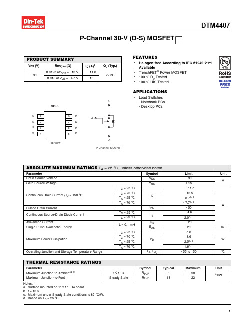
1P-Channel 30-V (D-S) MOSFETFEATURES•Halogen-free According to IEC 61249-2-21Available•T renchFET ® Power MOSFET •100 % R g Tested •100 % UIS TestedAPPLICATIONS•Load Switches - Notebook PCs - Desktop PCsPRODUCT SUMMARYV DS (V)R DS(on) (Ω)I D (A)d Q g (Typ.)- 300.0125 at V GS = - 10 V - 11.622 nC0.018 at V GS = - 4.5 V- 10Notes:a.Surface mounted on 1" x 1" FR4 board.b.t = 10 s.c.Maximum under Steady State conditions is 85 °C/W.d.Based on T C = 25 °C.ABSOLUTE MAXIMUM RATINGS T A = 25 °C, unless otherwise notedParameterSymbol Limit Unit Drain-Source Voltage V DS - 30VGate-Source VoltageV GS± 25Continuous Drain Current (T J = 150 °C)T C = 25 °C I D - 11.6AT C = 70 °C - 10.5T A = 25 °C - 8.7a, b T A = 70 °C - 7.7a, b Pulsed Drain CurrentI DM - 50Continuous Source-Drain Diode Current T C = 25 °C I S - 4.6T A = 25 °C 2.0a, b Avalanche CurrentL = 0.1 mH I AS - 20Single-Pulse Avalanche EnergyE AS 20mJMaximum Power Dissipation T C = 25 °C P D 5.6WT C = 70 °C 3.6T A = 25 °C 2.5a, b T A = 70 °C1.6a, b Operating Junction and Storage T emperature Range T J , T stg- 55 to 150°CTHERMAL RESISTANCE RATINGSParameterSymbol Typical MaximumUnit Maximum Junction-to-Ambient a, c t ≤ 10 s R thJA 3950°C/WMaximum Junction-to-FootSteady StateR thJF 1822S S D D D S GDSO-85678Top View23412Notes:a.Pulse test; pulse width ≤ 300 µs, duty cycle ≤ 2 %.b.Guaranteed by design, not subject to production testing.Stresses beyond those listed under “Absolute Maximum Ratings” may cause permanent damage to the device. These are stress ratings only, and functional operation of the device at these or any other conditions beyond those indicated in the operational sections of the specifications is not implied. Exposure to absolute maximum rating conditions for extended periods may affect device reliability.SPECIFICATIONS T J = 25 °C, unless otherwise notedParameter Symbol Test Conditions Min. Typ.Max.UnitStaticDrain-Source Breakdown Voltage V DS V GS = 0 V , I D = - 250 µA- 30V V DS Temperature Coefficient ΔV DS /T J I D = - 250 µA - 31mV/°C V GS(th) T emperature Coefficient ΔV GS(th)/T J 5.5Gate-Source Threshold Voltage V GS(th) V DS = V GS , I D = - 250 µA - 1.0- 3.0V Gate-Source LeakageI GSS V DS = 0 V , V GS = ± 25 V ± 100nA Zero Gate Voltage Drain Current I DSS V DS = - 30 V, V GS = 0 V - 1µA V DS = - 30 V, V GS = 0 V , T J = 55 °C- 5On-State Drain Current aI D(on) V DS ≥ - 10 V , V GS = - 10 V - 30A Drain-Source On-State Resistance a R DS(on)V GS = - 10 V , I D = - 10 A 0.0110.0125ΩV GS = - 4.5 V, I D = - 7 A 0.0120.018Forward T ransconductance a g fs V DS = - 10 V , I D = - 10 A23SDynamic bInput Capacitance C iss V DS = - 15 V , V GS = 0 V , f = 1 MHz1960pFOutput CapacitanceC oss 380Reverse Transfer Capacitance C rss 325Total Gate Charge Q g V DS = - 15 V, V GS = - 10 V , ID = - 10 A 4365nC V DS = - 15 V, V GS = - 4.5 V , I D = - 10 A 2233Gate-Source Charge Q gs 6Gate-Drain Charge Q gd 11Gate Resistance R g f = 1 MHz0.31.32.5ΩTurn-On Delay Time t d(on) V DD = - 15 V , R L = 3 ΩI D ≅ - 5 A, V GEN = - 10 V , R g = 1 Ω1122ns Rise Timet r 1325Turn-Off DelayTime t d(off) 3250Fall Timet f 918Turn-On Delay Time t d(on) V DD = - 15 V , R L = 3 ΩI D ≅ - 5 A, V GEN = - 4.5 V, R g = 1 Ω4470Rise Timet r 100160Turn-Off DelayTime t d(off) 2850Fall Timet f1530Drain-Source Body Diode Characteristics Continuous Source-Drain Diode Current I S T C = 25 °C- 4.6A Pulse Diode Forward Current I SM - 50Body Diode VoltageV SD I S = - 2 A, V GS = 0 V- 0.75- 1.2V Body Diode Reverse Recovery Time t rr I F = - 2 A, dI/dt = 100 A/µs, T J = 25 °C2845ns Body Diode Reverse Recovery Charge Q rr 2040nC Reverse Recovery Fall Time t a 13nsReverse Recovery Rise Timet b153CapacitanceOn-Resistance vs. Junction TemperatureThreshold Voltage Single Pulse Power, Junction-to-AmbientSafe Operating Area45TYPICAL CHARACTERISTICS 25°C, unless otherwise noted*The power dissipation P D is based on T J(max) = 150 °C, using junction-to-case thermal resistance, and is more useful in settling the upper dissipation limit for cases where additional heatsinking is used. It is used to determine the current rating, when this rating falls below the package limit.Current Derating*TYPICAL CHARACTERISTICS 25 °C, unless otherwise notedNormalized Thermal Transient Impedance, Junction-to-Foot 61DIM MILLIMETERSINCHESMin Max Min Max A 1.35 1.750.0530.069A 10.100.200.0040.008B 0.350.510.0140.020C 0.190.250.00750.010D 4.80 5.000.1890.196E 3.804.000.1500.157e 1.27 BSC0.050 BSCH 5.80 6.200.2280.244h 0.250.500.0100.020L 0.500.930.0200.037q 0°8°0°8°S0.440.640.0180.026ECN: C-06527-Rev. I, 11-Sep-06DWG: 54981A P P L I C A T I O N N O T ERECOMMENDED MINIMUM PADS FOR SO-8。

商品说明书产品的包装和配件清单商品说明书尊敬的用户:感谢您购买我们的产品。
为了让您更好地了解商品的包装和配件,请仔细阅读本商品说明书。
一、包装我们的商品采用精美的包装,旨在确保商品在运输过程中的安全和完好无损。
包装材料选用环保材料,符合相关法规和标准,同时具备良好的防摔、防潮和防尘功能。
商品的包装设计简洁大方,体现了产品的高品质和独特之处。
二、配件清单以下是本商品所附赠的配件及其详情:1. 电源适配器- 输入电压:220V-240V- 输出电压:5V- 输出电流:2A- 插头类型:国标插头(可根据您的需求提供适配器)2. 数据线- 长度:1.5米- 接口类型:USB-A 至 USB-C- 适用范围:可用于连接设备和充电3. 耳机- 接口类型:3.5mm 耳机插孔- 频率响应范围:20Hz-20kHz- 阻抗:32Ω- 线材长度:1.2米4. 保修卡- 保修期限:一年- 保修范围:自然损坏、非人为损坏的故障请注意,以上配件根据不同产品型号和配置可能会有所变化,具体配件清单以实际商品为准。
三、其他注意事项1. 请在使用前仔细阅读产品说明书,并按照说明书的指引正确使用商品及附件。
2. 如出现配件缺失或包装破损的情况,请立即联系销售商或售后服务中心进行处理。
3. 不要将商品包装材料随意丢弃,应当根据当地的环保规定进行正确的处理。
如需了解更多关于本商品的信息,请查阅产品介绍手册或访问官方网站。
如有疑问或需要进一步的技术支持,请随时联系我们的客服团队。
再次感谢您对我们产品的支持和信赖,我们将持续为您提供优质的商品和服务。
谢谢!附注:本商品说明书仅适用于指定产品,请勿将其用于其他用途或商品。
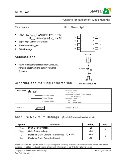
ANPEC reserves the right to make changes to improve reliability or manufacturability without notice, and advise customers to obtain the latest version of relevant information to verify before placing orders.Pin DescriptionOrdering and Marking InformationFeaturesApplications• Power Management in Notebook Computer,Portable Equipment and Battery Powered SystemsSO − 8• -30V/-4.6A, R DS(ON) = 52m Ω(typ.) @ V GS = -10VR DS(ON) = 80m Ω(typ.) @ V GS = -4.5V• Super High Density Cell Design • Reliable and Rugged • SO-8 PackageAbsolute Maximum Ratings (T A = 25°C unless otherwise noted)S S S GDD D D P-Channel MOSFETGA P M 9435H a n d lin g C o d e T e m p. R a n g e P a c k a g e C o d eP a c k a g e C o d e K : S O -8O p e ra tio n J u n c tio n T e m p. R a n g e C : -55 to 150°C H a n d lin g C o d e T U : T u b eT R : T a p e & R e e lA P M 9435A P M 9435X X X X XX X X X X - D a te C o d eElectrical Characteristics (T A = 25°C unless otherwise noted)Absolute Maximum Ratings (T A = 25°C unless otherwise noted)Notesa : Guaranteed by design, not subject to production testing b: Pulse test ; pulse width ≤300µs, duty cycle ≤ 2%0.02.55.07.510.012.515.017.520.00.000.020.040.060.080.100.120.140.1602468105101520-50-2502550751001251500.000.250.500.751.001.251.50123455101520Typical Characteristics-I D -D r a i n C u r r e n t (A )Transfer Characteristics-V GS - Gate-to-Source Voltage (V)Threshold Voltage vs. Junction T emperatureTj - Junction T emperature (°C)-V G S (t h )-T h r e s h o l d V o l t a g e (V )(N o r m a l i z e d )On-Resistance vs. Drain Current-I D - Drain Current (A)R D S (o n )-O n -R e s i s ta n c e (Ω)Output Characteristics-I D -D r a i n C u r r e n t (A )-V DS- Drain-to-Source Voltage (V)0510********200400600800123456789100.000.050.100.150.200.250.3005101520250246810-50-2502550751001251500.000.250.500.751.001.251.501.752.00Typical Characteristics-V GS - Gate-to-Source Voltage (V)R D S (o n )-O n -R e s i s t a n c e (Ω)On-Resistance vs. Gate-to-Source VoltageR D S (o n )-O n -R e s i s t a n c e (Ω)(N o r m a l i z e d )On-Resistance vs. Junction TemperatureT J - Junction T emperature (°C)-V DS - Drain-to-Source Voltage (V)CapacitanceC a p a c i t a n c e (p F )Gate ChargeQ G - Gate Charge (nC)-V G S -G a t e -S o u r c e V o l t a g e (V )0.010.111001020304050607080301E-41E-30.010.11100.010.11300.00.20.40.60.8 1.0 1.2 1.4 1.6 1.80.111020Typical CharacteristicsSingle Pulse Power Time (sec)Square Wave Pulse Duration (sec)N o r m a l i z e d E f f e c t i v e T r a n s i e n tT h e r m a l I m p e d a n c eNormalized Thermal Transient Impedence, Junction to AmbientP o w e r (W )Source-Drain Diode Forward Voltage-V SD -Source-to-Drain Voltage (V )-I S -S o u r c e C u r r e n t (Α)Packaging InformationSOP-8 pin ( Reference JEDEC Registration MS-012)Reflow Condition (IR/Convection or VPR Reflow)Physical SpecificationsPre-heat temperature183 CPeak temperatureTime°t e m p e r a t u r eClassification Reflow ProfilesPackage Reflow ConditionsReliability test programCover Tape DimensionsCustomer ServiceAnpec Electronics Corp.Head Office :5F, No. 2 Li-Hsin Road, SBIP,Hsin-Chu, Taiwan, R.O.C.T el : 886-3-5642000Fax : 886-3-5642050Taipei Branch :7F, No. 137, Lane 235, Pac Chiao Rd.,Hsin Tien City, Taipei Hsien, Taiwan, R. O. C.T el : 886-2-89191368Fax : 886-2-89191369。

tu933规格书摘要:1.背景介绍2.产品概述3.产品规格4.产品优势5.应用场景6.市场前景正文:随着科技的飞速发展,市场上涌现出越来越多的创新产品。
在此背景下,本文将为您介绍一款具有高性能、实用性的产品——tu933。
接下来,我们将从产品概述、规格、优势、应用场景和市场前景五个方面为您详细剖析这款产品。
一、背景介绍在智能化、信息化时代的推动下,人们对于电子产品的需求日益增长,对产品性能和功能的要求也越来越高。
为了满足市场需求,厂商们不断研发新产品,提升产品性能。
tu933就是在这样的背景下应运而生的一款高性能产品。
二、产品概述tu933是一款集多种功能于一体的电子产品。
它具备出色的性能,可以为用户提供高效、便捷的服务。
此外,tu933在外观设计上也颇具匠心,简约时尚,深受消费者喜爱。
三、产品规格tu933的规格非常齐全,包括以下几个方面:1.处理器:采用高性能处理器,运行速度快,能够满足用户多种需求。
2.内存:配置大容量内存,保障系统流畅运行,轻松应对多任务处理。
3.存储:提供大容量存储空间,让用户随心所欲地存储文件、图片、视频等。
4.显示器:采用高清晰度显示器,呈现细腻画质,带给用户优质的视觉体验。
5.电池:配备长寿命电池,续航能力强,满足用户全天候使用需求。
四、产品优势tu933具备以下优势:1.高性能:采用高性能处理器和内存,确保产品在运行大型软件和多任务处理时依然流畅。
2.便捷功能:具备丰富的接口和扩展能力,方便用户连接各种设备和使用第三方软件。
3.省电设计:采用低功耗技术,延长产品续航时间,减少用户充电次数。
4.安全性:具备严密的安全防护措施,保护用户数据和隐私。
5.价格合理:tu933在性能与品质上具有较高竞争力,价格相对实惠。
五、应用场景tu933适用于多种场景,如:1.商务办公:处理文档、演示、邮件等任务,提高工作效率。
2.学习研究:查阅资料、撰写论文、在线学习等。
3.娱乐休闲:观看高清视频、玩游戏、听音乐等。
1PRODUCT SUMMARYV DS (V)R DS(on) (Ω)I D (A)Q g (Typ.)- 200.018 at V GS = - 4.5 V - 6a 20 nC 0.026 at V GS = - 2.5 V - 6a 0.065 at V GS = - 1.8 V- 4Notes:a.Package limited.b.Surface Mounted on 1" x 1" FR4 board.c.t = 5 s.d .Rework Conditions: manual soldering with a soldering iron is not recommended for leadless components.e .Maximum under Steady State conditions is 80 °C/W.ABSOLUTE MAXIMUM RATINGS T A = 25 °C, unless otherwise notedParameterSymbol Limit Unit Drain-Source Voltage V DS - 20VGate-Source VoltageV GS± 12Continuous Drain Current (T J = 150 °C)T C = 25 °C I D - 6a AT C = 70 °C - 6a T A = 25 °C - 5b, c T A = 70 °C- 4.1b, c Pulsed Drain CurrentI DM - 50Continuous Source-Drain Diode CurrentT C = 25 °C I S- 6a T A = 25 °C - 2.9b, c Maximum Power DissipationT C = 25 °C P D 19WT C = 70 °C 12T A = 25 °C 3.5b, c T A = 70 °C 2.2b, c Operating Junction and Storage T emperature Range T J , T stg- 55 to 150°CSoldering Recommendations (Peak Temperature)d, e260THERMAL RESISTANCE RATINGSParameterSymbol Typical Maximum Unit Maximum Junction-to-Ambient b, e t ≤ 5 s R thJA 2836°C/WMaximum Junction-to-Case (Drain)Steady StateR thJC 5.3 6.5FEATURES•Halogen-free According to IEC 61249-2-21Definition•TrenchFET ® Power MOSFET •100 % R g Tested•Built in ESD Protection with Zener Diode •Typical ESD Performance: 1800 V•Compliant to RoHS Directive 2002/95/EC2Notes:a.Pulse test; pulse width ≤ 300 µs, duty cycle ≤ 2 %.b.Guaranteed by design, not subject to production testing.Stresses beyond those listed under “Absolute Maximum Ratings” may cause permanent damage to the device. These are stress ratings only, and functional operation of the device at these or any other conditions beyond those indicated in the operational sections of the specifications is not implied. Exposure to absolute maximum rating conditions for extended periods may affect device reliability.SPECIFICATIONS T J = 25 °C, unless otherwise notedParameter Symbol Test Conditions Min.Typ.Max.UnitStaticDrain-Source Breakdown Voltage V DS V GS = 0 V , I D = - 250 µA- 20V V DS Temperature Coefficient ΔV DS /T J I D= - 250 µA - 12mV/°C V GS(th) Temperature Coefficient ΔV GS(th)/T J 3Gate-Source Threshold Voltage V GS(th) V DS = V GS , I D = - 250 µA - 0.5- 1.2VGate-Source LeakageI GSS V DS = 0 V , V GS = ± 12 V ± 20µAV DS = 0 V , V GS = ± 4.5 V ± 0.5Zero Gate Voltage Drain Current I DSS V DS = - 20 V, V GS = 0 V - 1V DS = - 20 V , V GS = 0 V, T J = 55 °C- 10On-State Drain Current aI D(on)V DS ≤ - 5 V , V GS = - 4.5 V - 20A Drain-Source On-State Resistance a R DS(on) V GS = - 4.5 V, I D = - 5.6 A 0.0150.018ΩV GS = - 2.5 V, I D = - 5.3 A 0.0210.026V GS = - 1.8 V , I D = - 2.5 A 0.0400.065Forward T ransconductance a g fsV DS = - 10 V, I D = - 5.6 A35S Dynamic bTotal Gate Charge Q g V DS = - 10 V, V GS = - 8 V, I D = - 5 A 5075nCGate-Source Charge V DS = - 10 V, V GS = - 4.5 V, I D = - 5 A2030Q gs 3.3Gate-Drain Charge Q gd 8.4Gate Resistance R g f = 1 MHz0.212k ΩTurn-On Delay Time t d(on) V DD = - 10 V, R L = 1 Ω I D ≅ - 5 A, V GEN = - 4.5 V, R g = 1Ω0.71 1.1us Rise Timet r 1.7 2.6Turn-Off Delay Time t d(off) 69Fall Timet f 3.25Turn-On Delay Time t d(on) V DD = - 10 V, R L = 1 Ω I D ≅ - 5 A, V GEN = - 10 V, R g = 1Ω0.30.45Rise Timet r 0.60.9Turn-Off Delay Time t d(off) 1015Fall Timet f3.55.5Drain-Source Body Diode Characteristics Continuous Source-Drain Diode Current I S T C = 25 °C- 6A Pulse Diode Forward Current I SM - 50Body Diode VoltageV SD I S = - 5 A, V GS = 0 V- 0.85- 1.2V Body Diode Reverse Recovery Time t rr I F = 6 A, dI/dt = 100 A/µs, T J = 25 °C3060ns Body Diode Reverse Recovery Charge Q rr 2040nC Reverse Recovery Fall Time t a 13nsReverse Recovery Rise Timet b173Transfer CharacteristicsGate Charge4TYPICAL CHARACTERISTICS 25°C, unless otherwise notedOn-Resistance vs. Gate-to-Source VoltageSingle Pulse Power, Junction-to-AmbientThreshold VoltageSafe Operating Area, Junction-to-Ambient5TYPICAL CHARACTERISTICS 25*The power dissipation P D is based on T J(max) = 150 °C, using junction-to-case thermal resistance, and is more useful in settling the upper dissipation limit for cases where additional heatsinking is used. It is used to determine the current rating, when this rating falls below the package limit.Current Derating*TYPICAL CHARACTERISTICS 25°C, unless otherwise notedNormalized Thermal Transient Impedance, Junction-to-Case 61SOT-23 (TO-236): 3-LEADDimMILLIMETERS INCHESMinMaxMinMaxA 0.89 1.120.0350.044A 10.010.100.00040.004A 20.88 1.020.03460.040b 0.350.500.0140.020c0.0850.180.0030.007D 2.803.040.1100.120E 2.10 2.640.0830.104E 1 1.201.400.0470.055e 0.95 BSC 0.0374 Ref e 1 1.90 BSC0.0748 RefL 0.400.600.0160.024L 10.64 Ref 0.025 Ref S 0.50 Ref0.020 Refq3°8°3°8°ECN: S-03946-Rev. K, 09-Jul-01DWG: 54791A P P L I C A T I O N N O T ERECOMMENDED MINIMUM PADS FOR SOT-23。
1P-Channel 40-V (D-S) MOSFETFEATURES•Halogen-free According to IEC 61249-2-21Definition•TrenchFET ® Power MOSFET •100 % R g and UIS Tested•Compliant to RoHS Directive 2002/95/ECAPPLICATIONS•Power Switch•Load Switch in High Current Applications •DC/DC ConvertersPRODUCT SUMMARYV DS (V)R DS(on) (Ω)I D (A)Qg (Typ.)- 400.012 at V GS = - 10 V - 60d 600.018 at V GS = - 4.5 V- 48dTO-252SGDNotes:a.Duty cycle ≤ 1 %.b.See SOA curve for voltage derating.c.When Mounted on 1" square PCB (FR-4 material).d.Package limited.ABSOLUTE MAXIMUM RATINGS T C = 25 °C, unless otherwise notedParameterSymbol Limit Unit Drain-Source Voltage V DS - 40VGate-Source VoltageV GS± 20Continuous Drain Current (T J = 150 °C)T C = 25 °C I D - 60d AT C = 70 °C- 60d Pulsed Drain Current I DM - 100Avalanche Current I AS- 46Single Avalanche Energy a L = 0.1 mH E AS 106mJ Maximum Power DissipationaT C = 25 °C P D 73.5b W T A = 25 °C c2.5Operating Junction and Storage T emperature RangeT J , T stg- 55 to 150°CTHERMAL RESISTANCE RATINGSParameterSymbol Limit Unit Junction-to-Ambient (PCB Mount)c R thJA 50°C/WJunction-to-Case (Drain)R thJC1.72Notes:a.Pulse test; pulse width ≤ 300 µs, duty cycle ≤ 2 %.b.Guaranteed by design, not subject to production testing.c.Independent of operating temperature.Stresses beyond those listed under “Absolute Maximum Ratings” may cause permanent damage to the device. These are stress ratings only, and functional operation of the device at these or any other conditions beyond those indicated in the operational sections of the specifications is not implied. Exposure to absolute maximum rating conditions for extended periods may affect device reliability.SPECIFICATIONS T J = 25 °C, unless otherwise notedParameter Symbol Test Conditions Min.Typ.Max.UnitStaticDrain-Source Breakdown Voltage V DS V DS = 0 V , I D = - 250 µA - 40V Gate Threshold Voltage V GS(th) V DS = V GS , I D = - 250 µA - 1- 2.5Gate-Body LeakageI GSS V DS = 0 V, V GS = ± 20 V ± 250nA Zero Gate Voltage Drain Current I DSS V DS = - 40 V , V GS = 0 V - 1µA V DS = - 40 V , V GS = 0 V , T J = 125 °C - 50V DS = - 40 V , V GS = 0 V , T J = 150 °C- 250On-State Drain Current aI D(on)V DS ≤ - 10 V , V GS = - 10 V - 50ADrain-Source On-State Resistance a R DS(on) V GS = - 10 V, I D = - 22 A 0.0100.012ΩV GS = - 4.5 V , I D = - 19 A 0.0150.018Forward T ransconductance a g fs V DS = - 15 V , I D = - 22 A45SDynamic bInput Capacitance C iss V GS = 0 V , V DS = - 20 V , f = 1 MHz5380pFOutput CapacitanceC oss 570Reverse Transfer Capacitance C rss 500Total Gate Charge c Q g V DS = - 20 V , V GS = - 10 V , ID = - 20 A 106159nCV DS = - 20 V, V GS = - 4.5 V , I D = - 20 A 6090Gate-Source Charge cQ gs 22Gate-Drain Charge c Q gd 27Gate Resistance R g f = 1 MHz0.41.8 3.6ΩTurn-On Delay Time c t d(on) V DD = - 20 V , R L = 2 ΩI D ≅ - 10 A, V GEN = - 10 V , R g = 1 Ω1523nsRise Time ct r 1218Turn-Off Delay Time c t d(off) 70105Fall Time ct f 1827Drain-Source Body Diode Ratings and Characteristics T C = 25°C b Continuous Current I S - 60A Pulsed Current I SM - 100Forward Voltage a V SD I F = - 10 A, V GS = 0 V- 0.8- 1.5V Reverse Recovery Time t rr I F = - 10 A, dI/dt = 100 A/µs 3553ns Peak Reverse Recovery Current I RM(REC)- 2- 3A Reverse Recovery ChargeQ rr3350nCTransconductance On-Resistance vs. Gate-to-Source VoltageGate Charge3TYPICAL CHARACTERISTICS 25Source-Drain Diode Forward VoltageCapacitanceOn-Resistance vs. Junction TemperatureThreshold VoltageDrain Source Breakdown vs. Junction Temperature4TYPICAL CHARACTERISTICS 25°C, unless otherwise notedSingle Pulse Avalanche Current Capability vs. TimeSafe Operating Area51TO-252AA CASE OUTLINENote•Dimension L3 is for reference only.MILLIMETERSINCHESDIM.MIN.MAX.MIN.MAX.A 2.18 2.380.0860.094A1-0.127-0.005b 0.640.880.0250.035b20.76 1.140.0300.045b3 4.95 5.460.1950.215C 0.460.610.0180.024C20.460.890.0180.035D 5.97 6.220.2350.245D1 5.21-0.205-E 6.35 6.730.2500.265E1 4.32-0.170-H 9.4010.410.3700.410e 2.28 BSC 0.090 BSC e1 4.56 BSC 0.180 BSC L 1.40 1.780.0550.070L30.89 1.270.0350.050L4- 1.02-0.040L51.141.520.0450.060ECN: X12-0247-Rev. M, 24-Dec-12DWG: 5347RECOMMENDED MINIMUM PADS FOR DPAK (TO-252)1。
For other values & Custom Designs, contact factory.Specifications subject to change without notice.15801 Chemical Lane, Huntington Beach, CA 92649-1595Tel: (714) 898-0960 • Fax: (714) 896-0971RhombusIndustries Inc.35Electrical Specifications 1,2 at 25O CTurns Ratio ( + 5 % )PRI-SEC C W/W max.( pF )Leakage L L max.( µH )OCLmin.( mH )Pri. DCR max.(Ω )Sec. DCR max.(Ω )Schem.StyleT-941T-9711CT:11.2450.60.70.720E T-942T-9721CT:1.3CT 1.2450.60.70.920C T-943T-9731CT:2.1CT0.8350.40.6 1.412C T-944T-9741CT:5CT 1.2450.60.7 3.520C T-945T-9751CT:1CT 1.2450.60.70.720CT6-Pkg.Part Number Wide-SMDPartNumber*Due to High ET Product, these parts are recommended for all applications where FS is High, Open, or Low.1.Primary Pins for all parts listed are pins 1-5.2.Temp range is -40O C to +85O CPulse T ransformers for Maxim "MAX253"Thru-hole & Surface MountSchematic"E"Schematic "C"RS-485 Data Interface Applications RS-232 Data Interface Applications 1800 V RMS Minimum Isolation Custom Designs and Variations on electrical data availableET *min.(V-µS)1.Primary Pins for all parts listed are pins 1-5.2.Temp range is -40O C to +85O C**Due to lower ET Product, these parts are only recommendedfor applications where FS is High or Open..205(5.21)MAX.(0.30) TYP..012 .315(8.00)MAX..120(3.05)MIN..300(7.62) .285(7.24)MAX..020(0.51)TYP..100(2.54)TYP..050(1.27)TYP..010(0.25)TYP..008 R (0.20) .365(9.27)MAX.6-Pin DIP Package T-941 thru T-9456-Pin SMD Package T-1106G thru T-1110G.200(5.08)MAX..020(0.38).315(8.00)MAX..038(0.96)TYP..100(2.54)TYP.TYP..405 (10.29).425 (10.80) .270(6.86).286(7.27) .010(0.25)TYP.SMD available on Tape & ReelMAXIM - 4/99.350(8.89)MAX..250 MAX.(6.35).080(2.03).020 DIA.(0.51)TYP..120 (3.05)MIN..100(2.54)TYP..500(12.70)MAX..340(8.64).400(10.16)"T6" Package T-941 thru T-945Physical Dimensionsinches (mm)MAX. .260(6.60) MAX..300(7.62)MAX..410 .020(0.51) .100(2.54)TYP..010(0.25).510 (12.95).480 (12.19)MAX..410(10.41).040(1.02)TYP.TYP.(10.41) TYP.Wide-SMD Package T-971 thru T-975SMD available on Tape & ReelT-1106T-1106G 1CT:11.2600.80.80.812E T-1107T-1107G 1CT:1.3CT 1.2600.80.8 1.012C T-1108T-1108G 1CT:2.1CT 0.8500.60.7 1.68C T-1110T-1110G 1CT:1CT 1.2600.80.80.812CElectrical Specifications 1,2 at 25O CTurns Ratio ( + 5 % )PRI-SEC C W/W max.( pF )Leakage L L max.( µH )OCLmin.( mH )Pri. DCR max.(Ω )Sec. DCR max.(Ω )Schem.StyleET **min.(V-µS)DIP Part Number SMDPartNumber元器件交易网。
FEATURES
•Halogen-free According to IEC 61249-2-21Definition
•TrenchFET ® Power MOSFET
•Compliant to RoHS Directive 2002/95/EC
PRODUCT SUMMARY
V DS (V)R DS(on) (Ω)I D (A)- 30
0.042 at V GS = - 10 V - 5.80.055 at V GS = - 6 V - 5.00.060 at V GS = - 4.5 V
- 4.4
S D S D S D G
D
SO-8
5
678Top View
234
1Notes:
a.Surface Mounted on 1" x 1" FR4 board.
ABSOLUTE MAXIMUM RATINGS T A = 25°C, unless otherwise noted
Parameter
Symbol 10 s Steady State Unit Drain-Source Voltage V DS - 30V
Gate-Source Voltage
V GS
± 20
Continuous Drain Current (T J = 150 °C)a T A = 25 °C I D - 5.8- 4.1A T A = 70 °C
- 4.6
- 3.2
Pulsed Drain Current
I DM - 30
Continuous Source Current (Diode Conduction)a I S
- 2.3- 1.1Maximum Power Dissipation
a
T A = 25 °C P D 2.5 1.3W T A = 70 °C
1.6
0.8
Operating Junction and Storage T emperature Range
T J , T stg
- 55 to 150°C
THERMAL RESISTANCE RATINGS
Parameter
Symbol Typical Maximum Unit Maximum Junction-to-Ambient a t ≤ 10 s R thJA 4050°C/W
Steady State 7095Maximum Junction-to-Foot (Drain)Steady State
R thJF
24
30
Notes:
a.Guaranteed by design, not subject to production testing.
b.Pulse test; pulse width ≤ 300 µs, duty cycle ≤ 2 %.
Stresses beyond those listed under “Absolute Maximum Ratings” may cause permanent damage to the device. These are stress ratings only, and functional operation of the device at these or any other conditions beyond those indicated in the operational sections of the specifications is not implied. Exposure to absolute maximum rating conditions for extended periods may affect device reliability.
SPECIFICATIONS T J = 25°C, unless otherwise noted
Parameter Symbol Test Conditions Min.Typ.a
Max.Unit
Static
Gate Threshold Voltage V GS(th) V DS = V GS , I D = - 250 µA - 1.0
- 3.0V
Gate-Body Leakage
I GSS V DS = 0 V , V GS = ± 20 V ± 100
nA Zero Gate Voltage Drain Current I DSS V DS = - 30 V , V GS = 0 V - 1µA V DS = - 30 V , V GS = 0 V , T J = 70 °C
- 5
On-State Drain Current b
I D(on)
V DS ≤ - 10 V , V GS = - 10 V - 20A
V DS ≤ - 5 V, V GS = - 4.5 V - 5
Drain-Source On-State Resistance b R DS(on) V GS = - 10 V , I D = - 5.8 A
0.0330.042Ω
V GS = - 6 V , I D = - 5 A 0.0430.055V GS = - 4.5 V , I D = - 4.4 A 0.0560.060
Forward T ransconductance b g fs V DS = - 15 V , I D = - 5.8 A 13S Diode Forward Voltage b V SD
I S = - 2.3 A, V GS = 0 V
- 0.8
- 1.1V Dynamic a
Total Gate Charge Q g V DS = - 15 V , V GS = - 10 V , I D = - 3.5 A
1624
nC
Gate-Source Charge Q gs 2.3Gate-Drain Charge Q gd 4.5Gate Resistance R g 8.8Ω
Turn-On Delay Time t d(on) V DD = - 15 V , R L = 15 Ω I D ≅ - 1 A, V GEN = - 10 V , R g = 6 Ω1425ns Rise Time
t r 1425Turn-Off Delay Time t d(off) 4270Fall Time
t f 3050Source-Drain Reverse Recovery Time
t rr
I F = - 1.2 A, dI/dt = 100 A/µs 30
60
TYPICAL CHARACTERISTICS 25°C, unless otherwise noted
Output Characteristics
On-Resistance vs. Drain Current
Transfer Characteristics
On-Resistance vs. Junction Temperature
TYPICAL CHARACTERISTICS 25°C, unless otherwise noted
Source-Drain Diode Forward Voltage
On-Resistance vs. Gate-to-Source Voltage
Safe Operating Area, Junction-to-Foot
TYPICAL CHARACTERISTICS 25°C, unless otherwise noted
Normalized Thermal Transient Impedance, Junction-to-Ambient
Normalized Thermal Transient Impedance, Junction-to-Foot
DIM MILLIMETERS
INCHES
Min Max Min Max A 1.35 1.750.0530.069A 10.100.200.0040.008B 0.350.510.0140.020C 0.190.250.00750.010D 4.80 5.000.1890.196E 3.80
4.00
0.150
0.157
e 1.27 BSC
0.050 BSC
H 5.80 6.200.2280.244h 0.250.500.0100.020L 0.500.930.0200.037q 0°8°0°8°S
0.440.64
0.018
0.026
ECN: C-06527-Rev. I, 11-Sep-06
DWG: 5498
A P P L I C A T I O N N O T E
RECOMMENDED MINIMUM PADS FOR SO-8。