
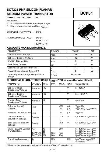
BCP51TA中文资料
- 格式:pdf
- 大小:42.85 KB
- 文档页数:1
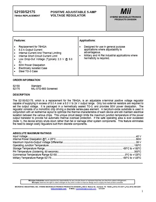
52150/52175POSITIVE ADJUSTABLE 5-AMP 78HGA REPLACEMENT VOLTAGE REGULATORMiiHYBRID MICROELECTRONICS PRODUCTS DIVISIONFeatures:•Replacement for 78HGA• 5.0 A Output Current•Internal Current And Thermal Limiting •Internal Short Circuit Current Limit•Low Drop-Out Voltage (Typically 2.3 V @ 5.0 A)•50W Power Dissipation•Electrically Isolated Case• Steel TO-3 Case Applications:•Designed for use in general purposeapplications where adjustability isadvantageous.•Military and Hi Rel Industrial applications where hermeticity is required.ORDER INFORMATION52150Standard52175MIL-STD-883 ScreenedDESCRIPTIONThe 52150/52175, which is a replacement for the 78HGA, is an adjustable 4-terminal positive voltage regulator capable of supplying in excess of 5.0 A over a 5.0 V to 24 V output range. Only two external resistors are required to set the output voltage. It is packaged in a hermetically sealed TO-3, and provides 50W power dissipation. The regulator consists of a monolithic chip driving a discrete series-pass element. A beryllium-oxide substrate is used in conjunction with an isothermal layout to optimize the thermal characteristics of each device and still maintain electrical isolation between the various chips. This unique circuit design limits the maximum junction temperature of the power output transistor to provide full automatic thermal overload protection. If the safe operating area is ever exceeded (Note 1), the device simply shuts down rather than fail or damage other system components. This feature eliminates the need to design costly regulators built from discrete components.ABSOLUTE MAXIMUM RATINGSInput Voltage.................................................................................................................................................................40 V Internal Power Dissipation @T c = 25°C.......................................................................................................................50W Maximum Input-to-Output Voltage Differential............................................................................................................35 V Operating Junction Temperature..............................................................................................................................150°C Storage Temperature Range...................................................................................................................-55°C to +150°C Pin Temperature (Soldering, 60 seconds)................................................................................................................300°C Commercial Temperature Range 52150.....................................................................................................0°C to +125°C Military Temperature Range 52175.........................................................................................................-55°C to +125°CMicropac Industries cannot assume any responsibility for any circuits shown or represent that they are free from patent infringement.52150/52175 POSITIVE ADJUSTABLE 5-AMP VOLTAGE REGULATORELECTRICAL CHARACTERISTICST J = 25ºC, V IN = 10 V and I OUT = -2.0A unless otherwise specifiedPARAMETER SYMBOL TEST CONDITIONS MIN TYP MAX UNIT Output Voltage (Note 4)V OUT I OUT = 2.0A,V IN = V OUT + 3.5V5.024VLine Regulation (Note 2)∆V OUT V IN= 7.5 to 25V0.2%1%V Load Regulation (Note 2)∆V OUT10mA ≤ I OUT ≤ 5.0A0.2%1%V Quiescent Current I Q I OUT = 0 3.410mA Ripple Rejection RR I OUT = 1.0A,f = 210Hz, 5.0V pk-pk60dBOutput Noise V n10Hz ≤ f ≤ 100 kHzV IN = V OUT + 5.0V50µV RMSDropout Voltage (Note 5)V DD I OUT = 5.0AI OUT = 3.0A 2.32.02.52.3VVShort-Circuit CurrentLimitI OS V IN= 15V, V OUT = 5V7.012.0A Control Pin Voltage V C 4.85 5.0 5.25VNOTES:1. This voltage regulator offers output transistor safe-area protection. However, to maintain full protection, thedevice must be operated within the maximum input-to-output voltage differential rating listed on the data sheet under “Absolute Maximum Ratings”. For applications violating these limits, device will not be fully protected.2. Load and line regulation are specified at constant junction temperature. Pulse testing is required with a pulsewidth ≤ 1 ms and a duty cycle ≤ 5%. Full Kelvin connection methods must be used to measure these parameters.3. The performance characteristics of the adjustable series (78HGA) is specified for V OUT = 5.0 V, unless otherwisenoted.4. V OUT is defined as V OUT = R1+ R2 (V CONT) where R1 and R2 are defined in the Basic Test Circuit diagram.5. Dropout Voltage is the input-output voltage differential that causes the output voltage to decrease by 5% of itsinitial value.Micropac Industries cannot assume any responsibility for any circuits shown or represent that they are free from patent infringement.52150/52175POSITIVE ADJUSTABLE 5-AMP VOLTAGE REGULATOR DESIGN CONSIDERATIONSThis device has thermal overload protection from excessive power and internal short circuit protection which limits the circuit’s maximum current. Thus, the device is protected from overload abnormalities. Although the internal power dissipation is limited, the junction temperature must be kept below the maximum specified temperature (150ºC). It is recommended by the manufacturer that the maximum junction temperature be kept as low as possible for increased reliability. To calculate the maximum junction temperature or heat sink required, the following thermal resistance values should be used.Package Type MaxP D(MAX) = T J(max) – T AθCA = θCS + θSAθJCθJCθ+ θCAJCTO-3 1.8 2.5Solving for T J = T A + P D (θJC+θCA)Where: T J = Junction TemperatureT A = Ambient TemperatureθCA = Case-to-ambient thermal resistanceP D = Power Dissipation θCS = Case-to-heat sink thermal resistanceθJC = Junction-to-case thermal resistanceθSA = Heat sink-to-ambient thermal resistance The device is designed to operate without external compensation components. However, the amount of external filtering of these voltage regulators depends upon the circuit layout. If in a specific application the regulator is more than four inches from the filter capacitor, a 2µF solid tantalum capacitor should be used at the input. A 1µF capacitor should be used at the output to reduce transients created by fast switching loads, as seen in the basic test circuit. These filter capacitors must be located as close to the regulator as possible.Caution: Permanent damage can result from forcing the output voltage higher than the input voltage. A protection diode from output to input should be used if this condition exists.VOLTAGE OUTPUTThe device has an adjustable output voltage from 5.0V to 24V which can be programmed by the external resistor network (potentiometer or two fixed resistors) using the relationship:Example: If R1 = 0Ω and R2 = 5kΩ, Then V OUT = V CONTROL x R1 + R2V OUT = 5V nominal.R2Or, if R1 = 10 kΩ and R2 = 5 kΩ thenV OUT = 15VMicropac Industries cannot assume any responsibility for any circuits shown or represent that they are free from patent infringement.。
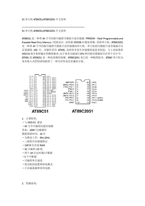
51单片机AT89C51/AT89C2051中文资料--------------------------------------------------------------------------------51单片机AT89C51/AT89C2051中文资料AT89C51是一种带4K字节闪烁可编程可擦除只读存储器(FPEROM—Falsh Programmable and Erasable Read Only Memory)的低电压,高性能CMOS8位微处理器,俗称单片机。
AT89C2051是一种带2K字节闪烁可编程可擦除只读存储器的单片机。
单片机的可擦除只读存储器可以反复擦除100次。
该器件采用ATMEL高密度非易失存储器制造技术制造,与工业标准的MCS-51指令集和输出管脚相兼容。
由于将多功能8位CPU和闪烁存储器组合在单个芯片中,ATMEL的A T89C51是一种高效微控制器,AT89C2051是它的一种精简版本。
AT89C单片机为很多嵌入式控制系统提供了一种灵活性高且价廉的方案。
1.主要特性:·与MCS-51 兼容·4K字节可编程闪烁存储器寿命:1000写/擦循环数据保留时间:10年·全静态工作:0Hz-24Hz·三级程序存储器锁定·128*8位内部RAM·32可编程I/O线·两个16位定时器/计数器·5个中断源·可编程串行通道·低功耗的闲置和掉电模式·片内振荡器和时钟电路2.管脚说明:VCC:供电电压。
GND:接地。
P0口:P0口为一个8位漏级开路双向I/O口,每脚可吸收8TTL门电流。
当P1口的管脚第一次写1时,被定义为高阻输入。
P0能够用于外部程序数据存储器,它可以被定义为数据/地址的第八位。
在FIASH编程时,P0 口作为原码输入口,当FIASH进行校验时,P0输出原码,此时P0外部必须被拉高。


54/742518选1数据选择器(3S,互补输出)简要说明:251为三态互补输出的8选1数据选择器,共有54/74251,54/74S251和54/74LS251三种线路结构型式,其主要电器特性的典型值如下(不同厂家具体值有差别):型号t PD(I到Z) P D54251/74251 17ns 260mW54S251/74S251 8ns 275mW54LS251/74LS251 17ns 38mW引出端符号:S0~S2 选择输入端E O输出使能(低电平有效)Z 输出/Z 反相输出端外接端口:逻辑图:双列直插封装极限值:电源电压 (7V)输入电压54/74251,54/74S251…………………………. 5.5V7V………………………………….54/74LS251输出高阻态时高电平电压 …………………………. 5.5V工作环境温度-55~125℃ 54XXX ………………………………….0~70℃74XXX ………………………………….存储温度 …………………………………………. -65~150℃功能表:推荐工作条件:54251/74251 54S251/74S251 54LS251/74LS251最小 额定最大最小额定最大最小 额定 最大单位54 4.5 5 5.5 4.5 5 5.5 4.5 5 5.5电源电压Vcc74 4.75 5 5.25 4.75 5 5.25 4.75 5 5.25V 输入高电平电V iH2 2 2 V 54 0.8 0.8 0.7输入低电平电V iL74 0.8 0.8 0.8 V 54 -2 -2 -1 输出高电平电流I OH74-5.2 -6.5 -2.6mA54 16 20 4输出低电平电流I OL74 16 20 8mA动态特性(T A =25℃)251 S251 LS251参 数【2】测 试 条 件 最大 最大 最大单位t PLH 45 18 45 t PHL 任一S 到Z(4级)45 19.5 45 nst PLH 33 15 33 t PHL 任一S 到/Z (3级) 33 13.5 33 ns t PLH 28 12 28 t PHL任一I 到ZVcc =5V R L =400Ω(S251为280Ω,LS251为2K) C L =50pF (S251和LS251为15pF) 28 12 28nst PLH 15 7 15t PHL 任一I 到/Z15 7 15 nst PZH 27 19.5 45 t PZL /EN 到Z 40 21 40 nst PZH 27 19.5 27t PZL /EN 到/Z C L =50pF (LS251为15pF)40 21 40 nst PHZ 8 8.5 45t PLZ /EN 到Z23 14 25 nst PHZ 8 8.5 56t PLZ/EN 到/ZC L =15pF23 14 25ns[2] t PLH 输出由低到高传输延迟时间t PHL 输出由高到低传输延迟时间 t PZH 输出由高阻态到高允许时间 t PZL 输出由高阻态到低允许时间 t PHZ 输出由高到高阻态禁止时间 t PLZ 输出由低到高阻态禁止时间静态特性(TA 为工作环境温度范围)251 S251 LS251参 数测 试 条 件【1】最小最大最小 最大 最小最大单位I ik =-12mA -1.5 V IK 输入嵌位电压Vcc=最小,I ik =-18mA -1.2 -1.5V V OH 输出高电平电压Vcc =最小,V IL =最大,V IH =2V, I OH =最大2.4 2.4 2.4 V 54 0.4 0.5 0.4 V OL 输出低电平电压Vcc=最小,V IL =最大,V IH =2V,I OL =最大74 0.4 0.5 0.5 V V I =5.5V 1 1 I I 最大输入电压时输入电流Vcc =最大V I =7V 0.1 mA V IH =2.4V 40I IH 输入高电平电流 Vcc =最大V IH =2.7V 50 20uA V IL =0.4V -1.6 -0.4I IL 输入低电平电流 Vcc =最大V IL =0.5V-2 mAI OS 输出短路电流 Vcc =最大-18 -55 -40 -100 -30 -130mA V O =2.4V 40 50I OZH 输出高阻态时高电平电流Vcc =最大,V IH =2V V O =2.7V 20 uAV O =0.4V-50 uAI OZL输出高阻态时低电平电流Vcc=最大,V IH=2V,V IL=最大V O=0.4V-50 uAV O=0.5V-20Icc电源电流 Vcc=最大 62 85 12 mA[1]: 测试条件中的“最小”和“最大”用推荐工作条件中的相应值。