2SA1952中文资料(rohm)中文数据手册「EasyDatasheet - 矽搜」
- 格式:pdf
- 大小:349.17 KB
- 文档页数:5
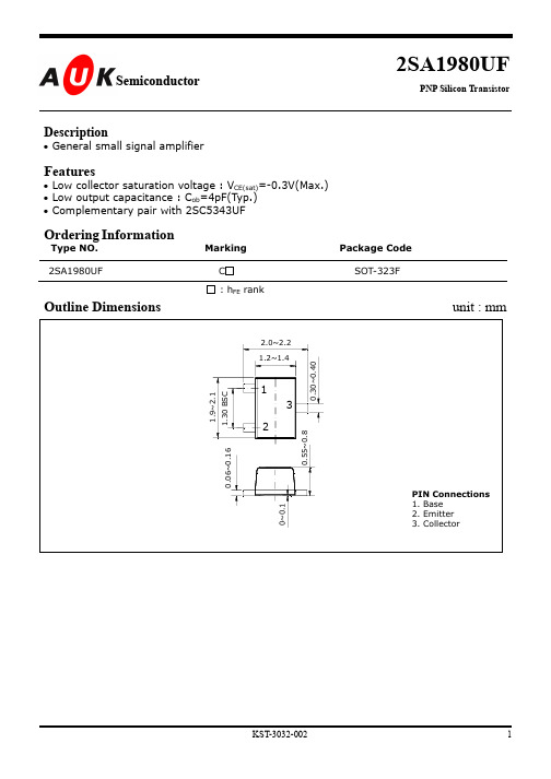
2SA1980UF S e m i c o n d u c t o rPNP Silicon TransistorAbsolute maximum ratings (Ta=25°C)Characteristic Symbol Ratings UnitCollector-Base voltage V CBO -50 V Collector-Emitter voltage V CEO -50 V Emitter-Base voltage V EBO -5 VCollector current I C -150 mA Collector dissipation P C 200 mWJunction temperature T j 150 °C Storage temperatureT stg -55~150 °CElectrical Characteristics (Ta=25°C)Characteristic SymbolTest Condition Min. Typ. Max.UnitCollector-Base breakdown voltage BV CBOI C =-100µA, I E =0 -50 - - V Collector-Emitter breakdown voltage BV CEO I C =-1mA, I B =0 -50 - - VEmitter-Base breakdown voltage BV EBO I E =-10µA, I C =0 -5 - - V Collector cut-off current I CBO V CB =-50V , I E =0 - - -0.1µA Emitter cut-off current I EBO V EB =-5V , I C =0 - - -0.1 µA DC current gainh FE *V CE =-6V , I C =-2mA 70 - 700 -Collector-Emitter saturation voltage V CE(sat) I C =-100mA, I B =-10mA - - -0.3 V Transition frequencyf T V CE =-10V , I C =-1mA 80 - - MHzCollector output capacitance C ob V CB =-10V , I E =0, f=1MHz -47pFNoise figureNFV CE =-6V , I C =-0.1mAf=1KHz, Rg=10K Ω- - 10 dB*: h FE rank / O : 70~140, Y : 120~240, G : 200~400, L : 300~700.Electrical Characteristic CurvesFig. 5 V CE(sat)-I CThese AUK products are intended for usage in general electronic equipments(Office and communication equipment, measuring equipment, domestic electrification, etc.).Please make sure that you consult with us before you use these AUK products in equipm-ents which require high quality and/or reliability, and in equipments which could have major impact to the welfare of human life(atomic energy control, airplane, spaceship, traffic signal, combustion central, all types of safety device, etc.).AUK cannot accept liability to any damage which may occur in case these AUK products were used in the mentioned equipments without prior consultation with AUK.。


2SA1774G, S2SA1774G PNP Silicon General Purpose Amplifier Transistor This PNP transistor is designed for general purpose amplifier applications. This device is housed in the SC−75/SOT−416/SC−90 package which is designed for low power surface mount applications, where board space is at a premium.Features•Reduces Board Space•High h FE, 210−460 (typical)•Low V CE(sat), < 0.5V•Available in 8mm, 7−inch/3000 Unit Tape and Reel•S Prefix for Automotive and Other Applications Requiring Unique Site and Control Change Requirements; AEC−Q101 Qualified and PPAP Capable•These Devices are Pb−Free, Halogen Free/BFR Free and are RoHS Compliant*MAXIMUM RATINGS (T A = 25°C)Rating Symbol Value Unit Collector − Emitter Voltage V(BR)CBO−60Vdc Collector − Base Voltage V(BR)CEO−50Vdc Emitter − Base Voltage V(BR)EBO−6.0Vdc Collector Current − Continuous I C−100mAdc THERMAL CHARACTERISTICSCharacteristic Symbol Max Unit Power Dissipation (Note 1)P D150mW Junction T emperature T J150°C Storage T emperature Range T stg−55 ~ +150°C Stresses exceeding Maximum Ratings may damage the device. MaximumRatings are stress ratings only. Functional operation above the Recommended Operating Conditions is not implied. Extended exposure to stresses above the RecommendedOperating Conditions may affect device reliability.1.Device mounted on a FR−4 glass epoxy printed circuit board using theminimum recommended footprint.*For additional information on our Pb−Free strategy and soldering details, please download the ON Semiconductor Soldering and Mounting T echniques ReferenceManual, SOLDERRM/D.MARKING DIAGRAMCOLLECTOR1BASE2EMITTERSC−75CASE 463STYLE 1F9= Device CodeM= Date Code*G= Pb−Free Package(Note: Microdot may be in either location)*Date Code orientation may vary dependingupon manufacturing location.Device Package Shipping†ORDERING INFORMATION2SA1774G SC−75(Pb−Free)3,000/T ape & Reel†For information on tape and reel specifications, including part orientation and tape sizes, please refer to our T ape and Reel Packaging Specifications Brochure, BRD8011/D.2SA1774T1G SC−75(Pb−Free)3,000/T ape & Reel S2SA1774G SC−75(Pb−Free)3,000/T ape & ReelELECTRICAL CHARACTERISTICS (T A = 25°C)Characteristic Symbol Min Typ Max UnitCollector−Base Breakdown Voltage (I C = −50 m Adc, I E = 0)V(BR)CBO−60−−VdcCollector−Emitter Breakdown Voltage (I C = −1.0 mAdc, I B = 0)V(BR)CEO−50−−VdcEmitter−Base Breakdown Voltage (I E = −50 m Adc, I E = 0)V(BR)EBO−6.0−−VdcCollector−Base Cutoff Current (V CB = −30 Vdc, I E = 0)I CBO−−−0.5nAEmitter−Base Cutoff Current (V EB = −5.0 Vdc, I B = 0)I EBO−−−0.5m ACollector−Emitter Saturation Voltage (Note 2) (I C = −50 mAdc, I B = −5.0 mAdc)V CE(sat)−−−0.5VdcDC Current Gain (Note 2)(V CE = −6.0 Vdc, I C = −1.0 mAdc)h FE120−560−Transition Frequency(V CE = −12 Vdc, I C = −2.0 mAdc, f = 30 MHz)f T−140−MHzOutput Capacitance(V CB = −12 Vdc, I E = 0 Adc, f = 1 MHz)C OB− 3.5−pFFigure 1. Collector −Emitter Saturation Voltagevs. Collector Current10.1I C , COLLECTOR CURRENT (mA)V C E , C O L L E C T O R −E M I T T E R S A T U R A T I O N V O L T A G E (V )Figure 2. Base −Emitter Saturation Voltage vs.Collector CurrentI C , COLLECTOR CURRENT (mA)V B E (s a t ), B A S E −E M I T T E R S A T U R A T I O N V O L T A G E (V )Figure 3. DC Current Gain vs. CollectorCurrentI C , COLLECTOR CURRENT (mA)h F E , D C C U R R E N T G A I NFigure 4. Saturation RegionI B , BASE CURRENT (mA)V C E (s a t ), C O L L E C T O R −E M I T T E R S A T U R A T I O N V O L T A G E (V )Figure 5. Base −Emitter Turn −ON Voltage vs.Collector CurrentI C , COLLECTOR CURRENT (mA)V B E (O N ), B A S E −E M I T T E R O N V O L T A G E (V )Figure 6. CapacitanceV R , REVERSE VOLTAGE (V)C , C A P A C I T A N C E (p F )10Figure 7. Current Gain Bandwidth Product vs.Collector CurrentI C , COLLECTOR CURRENT (mA)f t a u , C U R R E N T G A I N B A N D W I D T H P R O D U C T (M H z )Figure 8. Safe Operating AreaV CE , COLLECTOR EMITTER VOLTAGE (V)I C , C O L L E C T O R C U R R E N T (m A )PACKAGE DIMENSIONSSTYLE 1:PIN 1.BASE 2.EMITTER 3.COLLECTORSC −75/SOT −416CASE 463ISSUE FNOTES:1.DIMENSIONING AND TOLERANCING PER ANSI Y14.5M, 1982.2.CONTROLLING DIMENSION: MILLIMETER.DIM MIN NOM MAX MILLIMETERS A 0.700.800.90A10.000.050.10b C 0.100.150.25D 1.55 1.60 1.65E e 1.00 BSC 0.0270.0310.0350.0000.0020.0040.0040.0060.0100.0590.0630.0670.04 BSCMIN NOM MAX INCHES0.150.200.300.0060.0080.012H EL 0.100.150.201.50 1.60 1.700.0040.0060.0080.0610.0630.0650.700.800.900.0270.0310.035ǒmm inchesǓSCALE 10:1*For additional information on our Pb −Free strategy and solderingdetails, please download the ON Semiconductor Soldering and Mounting T echniques Reference Manual, SOLDERRM/D.SOLDERING FOOTPRINT*ON Semiconductor and are registered trademarks of Semiconductor Components Industries, LLC (SCILLC). SCILLC reserves the right to make changes without further notice to any products herein. SCILLC makes no warranty, representation or guarantee regarding the suitability of its products for any particular purpose, nor does SCILLC assume any liability arising out of the application or use of any product or circuit, and specifically disclaims any and all liability, including without limitation special, consequential or incidental damages. “Typical” parameters which may be provided in SCILLC data sheets and/or specifications can and do vary in different applications and actual performance may vary over time. All operating parameters, including “Typicals” must be validated for each customer application by customer’s technical experts. SCILLC does not convey any license under its patent rights nor the rights of others. SCILLC products are not designed, intended, or authorized for use as components in systems intended for surgical implant into the body,or other applications intended to support or sustain life, or for any other application in which the failure of the SCILLC product could create a situation where personal injury or death may occur. Should Buyer purchase or use SCILLC products for any such unintended or unauthorized application, Buyer shall indemnify and hold SCILLC and its officers, employees,subsidiaries, affiliates, and distributors harmless against all claims, costs, damages, and expenses, and reasonable attorney fees arising out of, directly or indirectly, any claim of personal injury or death associated with such unintended or unauthorized use, even if such claim alleges that SCILLC was negligent regarding the design or manufacture of the part.SCILLC is an Equal Opportunity/Affirmative Action Employer. This literature is subject to all applicable copyright laws and is not for resale in any manner.PUBLICATION ORDERING INFORMATION分销商库存信息: ONSEMIS2SA1774G。


TransistorsRev.A 1/3High speed switching transistor (60V, 5A)2SC5103z Features1) Low V CE(sat) (Typ. 0.15V at I C / I B = 3 / 0.15A) 2) High speed switching (tf : Typ. 0.1 µs at I C = 3A) 3) Wide SOA. (safe operating area) 4) Complements the 2SA1952.z Absolute maximum ratings (T a=25°C)ParameterSymbol V CBO V CEO V EBOI C P C Tj Tstg Limits 10060551150−55 to +150Unit V V V A(DC)10∗A(Pulse)W10W(Tc =25°C)°C °CSingle pulse Pw=100msCollector-base voltage Collector-emitter voltage Emitter-base voltage Collector current Junction temperature Storage temperatureCollector power dissipation∗z Packaging specifications and h FEType 2SC5103CPT3Q TL 2500Package h FE CodeBasic ordering unit (pieces)z External dimensions (Unit : mm)2.30.51.00.59.52.50.8Min.1.56.52.3(2)(3)C0.50.650.9(1)0.752.30.91.55.5(3) Emitter(2) Collector (1) Base ROHM : CPT3EIAJ : SC-635.1z Electrical characteristics (T a=25°C)TransistorsRev.A 2/3zElectrical characteristics curvesC O L L E C T O R C U R R E N T : I C (A )COLLECTOR TO EMITTER VOLTAGE : V CE (V)Fig.1 Ground emitter output characteristicsBASE TO EMITTER VOLTAGE : V BE (V)C O L L E C T O R C U R R E N T : I C (A )Fig.2 Ground emitter propagation characteristicsD C C U R RE N T G A I N : hF ECOLLECTOR CURRENT : I C (A)Fig.3 DC current gain vs. collector currentB A S E S A T U R A T I O N V O L T A G E : V B E (s a t ) (V )C O L L E C T O R S A T U R A T I O N V O L T A G E: V C E (s a t ) (V )COLLECTOR CURRENT : I C (A )Fig.4 Collector-emitter saturation voltageBase-emitter saturation voltage −collector currentC O L L E C T O R O U T P U T C A P A C I T W A N C E : C o b (p F )COLLECTOR TO BASE VOLTAGE : V CB (V)Fig.6 Collector output capacitance vs. collector-base voltage−T R A N S I T I O N F R E Q U E N C Y : f T (M H z )EMITTER CURRENT : I E (A)Fig.5 Gain bandwidth product vs.emitter currentS T R A G E T I M E : t s t g (µs )F A L LT I M E : t f (µs )T U R N O N T I M E : t o n (µs )COLLECTOR CURRENT : I C (A)Fig.7 Switching characteristicsCOLLECTOR TO EMITTER VOLTAGE : V CE (V)C O L L E C T O R C U R R E N T : I C (A )Fig.8 Safe operating areaTIME : t (s)T R A N S I E N T T H E R M A L R E S I S T A N C E : R t h (°C /W )Fig.9 Transient thermal resistanceTransistorsRev.A 3/3BBFig.10 Switching characteristic circuitAppendixAbout Export Control Order in JapanProducts described herein are the objects of controlled goods in Annex 1 (Item 16) of Export T rade ControlOrder in Japan.In case of export from Japan, please confirm if it applies to "objective" criteria or an "informed" (by MITI clause)on the basis of "catch all controls for Non-Proliferation of Weapons of Mass Destruction.Appendix1-Rev1.1。