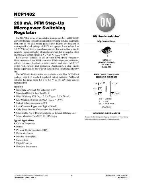
NCP1402200 mA, PFM Step−Up Micropower Switching RegulatorThe NCP1402 series are monolithic micropower step−up DC to DC converter that are specially designed for powering portable equipment from one or two cell battery packs.These devices are designed to start−up with a cell voltage of 0.8 V and operate down to less than 0.3V. With only three external components, this series allow a simple means to implement highly efficient converters that are capable of up to 200 mA of output current at V in = 2.0 V, V OUT = 3.0 V.Each device consists of an on−chip PFM (Pulse Frequency Modulation) oscillator, PFM controller, PFM comparator, soft−start, voltage reference, feedback resistors, driver, and power MOSFET switch with current limit protection. Additionally, a chip enable feature is provided to power down the converter for extended battery life.The NCP1402 device series are available in the Thin SOT−23−5 package with five standard regulated output voltages. Additional voltages that range from 1.8 V to 5.0 V in 100 mV steps can be manufactured.Features•Extremely Low Start−Up V oltage of 0.8 V•Operation Down to Less than 0.3 V•High Efficiency 85% (V in = 2.0 V, V OUT = 3.0 V, 70 mA)•Low Operating Current of 30 m A (V OUT = 1.9 V)•Output V oltage Accuracy ±2.5%•Low Converter Ripple with Typical 30 mV•Only Three External Components Are Required•Chip Enable Power Down Capability for Extended Battery Life •Micro Miniature Thin SOT−23−5 PackagesTypical Applications•Cellular Telephones•Pagers•Personal Digital Assistants (PDA)•Electronic Games•Portable Audio (MP3)•Camcorders•Digital Cameras•Handheld InstrumentsORDERING INFORMATIONSee detailed ordering and shipping information in the ordering information section on page 3 of this data sheet.Figure 1. Typical Step−Up Converter ApplicationV OUTV inOUT2NC 3GND4LX 5Figure 2. Representative Block DiagramPIN FUNCTION DESCRIPTIONSORDERING INFORMATIONNOTE: The ordering information lists five standard output voltage device options. Additional device with output voltage ranging from 1.8 V to 5.0 V in 100 mV increments can be manufactured. Contact your ON Semiconductor representative for availability.ABSOLUTE MAXIMUM RATINGSNOTES:1.This device series contains ESD protection and exceeds the following tests:Human Body Model (HBM) ±2.0 kV per JEDEC standard: JESD22−A114.Machine Model (MM) ±200 V per JEDEC standard: JESD22−A115.2.The maximum package power dissipation limit must not be exceeded.P D+T J(max)*T AR q JAtch−up Current Maximum Rating: ±150 mA per JEDEC standard: JESD78.4.Moisture Sensitivity Level: MSL 1 per IPC/JEDEC standard: J−STD−020A.SET6.CE pin is integrated with an internal 10 MΩ pull−up resistor.1006080402001.9604020V O U T , O U T P U T V O L T A G E (V )I O , OUTPUT CURRENT (mA)Figure 3. NCP1402SN19T1 Output Voltage vs.Output Current Figure 4. NCP1402SN30T1 Output Voltage vs.Output Current6.05.04.03.01.0V O U T , O U T P U T V O L T A G E (V )Figure 7. NCP1402SN30T1 Efficiency vs.Output Current I O , OUTPUT CURRENT (mA)Figure 8. NCP1402SN50T1 Efficiency vs.Output CurrentI O , OUTPUT CURRENT (mA)E F F I C I E N C Y (%)I O , OUTPUT CURRENT (mA)2.0801001201401601802000604020801001201401601802002.060402080100120140160180200604020801001201401601802001006080402002.0V O U T , O U T P U T V O L T A G E (V )1.65.25.15.04.94.84.7V O U T , O U T P U T V O L T A G E (V )Figure 13. NCP1402SN30T1 OperatingCurrent 1 vs. Temperature TEMPERATURE (°C)Figure 14. NCP1402SN50T1 OperatingCurrent 1 vs. TemperatureTEMPERATURE (°C)I D D 1, O P E R A T I N G C U R R E N T 1 (m A )2.11.71.81.9−50250−255075100−50250−255075100−506.5255.50−25t o n , S W I T C H O N T I M E (µs )5.0TEMPERATURE (°C)Figure 15. NCP1402SN19T1 Switch On Timevs. Temperature Figure 16. NCP1402SN30T1 Switch On Timevs. Temperature7.06.56.05.55.04.5t o n , S W I T C H O N T I M E (µs )Figure 19. NCP1402SN30T1 Minimum SwitchOff Time vs. Temperature TEMPERATURE (°C)Figure 20. NCP1402SN50T1 Minimum SwitchOff Time vs. TemperatureTEMPERATURE (°C)t o f f , M I N I M U M S W I T C H O F F T I M E (µs )7.5TEMPERATURE (°C)6.07.05075100−5025−255075100−5025−255075100−5025−2550751001.51.61.41.31.71.82502301902101701509060D M A X , M A X I M U M D U T Y C Y C L E (%)401007060905040Figure 25. NCP1402SN30T1 LX Pin On−StateCurrent vs. Temperature TEMPERATURE (°C)Figure 26. NCP1402SN50T1 LX Pin On−StateCurrent vs. TemperatureTEMPERATURE (°C)100507080−5025−255075100−5025−255075100D M A X , M A X I M U M D U T Y C Y C LE (%)80I L X , L X P I N O N −S T A T E C U R R E N T (m A )0.80.20.01.00.40.63.02.51.01.50.50.00.80.2V L X L I M , V L X V O L T A G E L I M I T (V )0.0V L X L I M , V L X V O L T A G E L I M I T (V )Figure 31. NCP1402SN30T1 Switch−onResistance vs. Temperature TEMPERATURE (°C)Figure 32. NCP1402SN50T1 Switch−onResistance vs. TemperatureTEMPERATURE (°C)R D S (o n ), S W I T C H −O N R E S I S T A N C E (Ω)1.00.40.6−5025−255075100−5025−2550751002.00.80.4V s t a r t /V h o l d , S T A R T U P /H O L D V O L T A G E (V )0.0Figure 37. NCP1402SN30T1 Startup/HoldVoltage vs. Output Current 1.00.20.6Figure 38. NCP1402SN50T1 Startup/HoldVoltage vs. Output Current0.80.4V s t a r t /V h o l d , S T A R T U P /H O L D V O L T A G E (V )0.01.00.20.6I O , OUTPUT CURRENT (mA)405030206010708090100I O , OUTPUT CURRENT (mA)V s t a r t /V h o l d , S T A R T U P /H O L D V O L T A G E (V )405030206010708090100Figure 39. NCP1402SN19T1 Operating Waveforms (Medium Load)Figure 40. NCP1402SN19T1 Operating Waveforms (Heavy Load)Figure 41. NCP1402SN30T1 Operating Waveforms (Medium Load)Figure 42. NCP1402SN30T1 Operating Waveforms (Heavy Load)Figure 43. NCP1402SN50T1 Operating Waveforms (Medium Load)Figure 44. NCP1402SN50T1 OperatingWaveforms (Heavy Load)V OUT = 1.9 V, V in = 1.2 V, I O = 30 mA, L = 47 m H, C OUT = 68 m F1.V LX, 1.0 V/div2.V OUT, 20 mV/div, AC coupled3.I L, 100 mA/div2 m s/divV OUT = 3.0 V, V in = 1.2 V, I O = 30 mA, L = 47 m H, C OUT = 68 m F1.V LX,2.0 V/div2.V OUT, 20 mV/div, AC coupled3.I L, 100 mA/div5 m s/divV OUT = 3.0 V, V in = 1.2 V, I O = 70 mA, L = 47 m H, C OUT = 68 m F1.V LX,2.0 V/div2.V OUT, 20 mV/div, AC coupled3.I L, 100 mA/divV OUT = 1.9 V, V in = 1.2 V, I O = 70 mA, L = 47 m H, C OUT = 68 m F1.V LX, 1.0 V/div2.V OUT, 20 mV/div, AC coupled3.I L, 100 mA/div5 m s/div2 m s/div2 m s/divV OUT = 5.0 V, V in = 1.5 V, I O = 30 mA, L = 47 m H, C OUT = 68 m F1.V LX,2.0 V/div2.V OUT, 20 mV/div, AC coupled3.I L, 100 mA/div2 m s/divV OUT = 5.0 V, V in = 1.5 V, I O = 60 mA, L = 47 m H, C OUT = 68 m F1.V LX,2.0 V/div2.V OUT, 20 mV/div, AC coupled3.I L, 100 mA/divFigure 45. NCP1402SN19T1 Load TransientResponse Figure 46. NCP1402SN19T1 Load TransientResponseFigure 47. NCP1402SN30T1 Load TransientResponse Figure 48. NCP1402SN30T1 Load TransientResponseFigure 49. NCP1402SN50T1 Load TransientResponse Figure 50. NCP1402SN50T1 Load TransientResponseV in = 1.2 V, L = 47 m H, C OUT = 68 m F1.V OUT = 1.9 V (AC coupled), 100 mV/div2.I O = 0.1 mA to 80 mAV in = 1.2 V, L = 47 m H, C OUT = 68 m F1.V OUT = 1.9 V (AC coupled), 100 mV/div2.I O = 80 mA to 0.1 mAV in = 2.4 V, L = 47 m H, C OUT = 68 m F1.V OUT = 5.0 V (AC coupled), 100 mV/div2.I O = 0.1 mA to 80 mAV in = 2.4 V, L = 47 m H, C OUT = 68 m F1.V OUT = 5.0 V (AC coupled), 100 mV/div2.I O = 80 mA to 0.1 mAV in = 1.5 V, L = 47 m H, C OUT = 68 m F1.V OUT = 3.0 V (AC coupled), 100 mV/div2.I O = 0.1 mA to 80 mAV in = 1.5 V, L = 47 m H, C OUT = 68 m F1.V OUT = 3.0 V (AC coupled), 100 mV/div2.I O = 80 mA to 0.1 mA60V r i p p l e , R I P P L E V O L T A G E (m V )Figure 55. NCP1402SNXXT1 Pin On−stateCurrent vs. Output Voltage Figure 56. NCP1402SNXXT1 Switch−OnResistance vs. Output Voltage80204010060V r i p p l e , R I P P L E V O L T A G E (m V )0802040100V OUT , OUTPUT VOLTAGE (V)134256V OUT , OUTPUT VOLTAGE (V)I L X , L X P I N O N −S T A T E C U R R E N T (m A )134252201002601401803006125321I i n (n o l o a d ), N O L O A D I N P U T C U R R E N T (µA )V in , INPUT VOLTAGE (V)Figure 57. NCP1402SNXXT1 No Load InputCurrent vs. Input Voltage Figure 58. NCP1402SNXXT1 Maximum OutputCurrent vs. Input Voltage150V in , INPUT VOLTAGE (V)25507510045612345DETAILED OPERATING DESCRIPTIONOperationThe NCP1402 series are monolithic power switching regulators optimized for applications where power drain must be minimized. These devices operate as variable frequency, voltage mode boost regulators and designed to operate in continuous conduction mode. Potential applications include low powered consumer products and battery powered portable products.The NCP1402 series are low noise variable frequency voltage−mode DC−DC converters, and consist of soft−start circuit, feedback resistor, reference voltage, oscillator, PFM comparator, PFM control circuit, current limit circuit and power switch. Due to the on−chip feedback resistor network,the system designer can get the regulated output voltage from 1.8 V to 5 V with a small number of external components. The operating current is typically 30 m A (V OUT = 1.9 V), and can be further reduced to about 0.6 m A when the chip is disabled (V CE < 0.3 V).The NCP1402 operation can be best understood by examining the block diagram in Figure 2. PFM comparator monitors the output voltage via the feedback resistor. When the feedback voltage is higher than the reference voltage, the power switch is turned off. As the feedback voltage is lower than reference voltage and the power switch has been off for at least a period of minimum off−time decided by PFM oscillator, the power switch is then cycled on for a period of on−time also decided by PFM oscillator, or until current limit signal is asserted. When the power switch is on, current ramps up in the inductor, storing energy in the magnetic field. When the power switch is off, the energy in the magnetic field is transferred to output filter capacitor and the load. The output filter capacitor stores the charge while the inductor current is high, then holds up the output voltage until next switching cycle.Soft StartThere is a soft start circuit in NCP1402. When power is applied to the device, the soft start circuit pumps up the output voltage to approximately 1.5 V at a fixed duty cycle, the level at which the converter can operate normally. What is more,the start−up capability with heavy loads is also improved.Regulated Converter Voltage (V OUT )The V OUT is set by an internal feedback resistor network.This is trimmed to a selected voltage from 1.8 to 5.0 V range in 100 mV steps with an accuracy of $2.5%.Current LimitThe NCP1402 series utilizes cycle−by−cycle current limiting as a means of protecting the output switch MOSFET from overstress and preventing the small value inductor from saturation. Current limiting is implemented by monitoring the output MOSFET current build−up during conduction, and upon sensing an overcurrent conduction immediately turning off the switch for the duration of the oscillator cycle.The voltage across the output MOSFET is monitored and compared against a reference by the VLX limiter. When the threshold is reached, a signal is sent to the PFM controller block to terminate the power switch conduction. The current limit threshold is typically set at 350 mA.Enable / Disable OperationThe NCP1402 series offer IC shut−down mode by chip enable pin (CE pin) to reduce current consumption. An internal pull−up resistor tied the CE pin to OUT pin by default i.e. user can float the pin CE for permanent “On”.When voltage at pin CE is equal or greater than 0.9 V , the chip will be enabled, which means the regulator is in normal operation. When voltage at pin CE is less than 0.3 V , the chip is disabled, which means IC is shutdown.Important: DO NOT apply a voltage between 0.3 V and 0.9 V to pin CE as this is the CE pin’s hyteresis voltagerange. Clearly defined output states can only be obtained by applying voltage out of this range.APPLICATIONS CIRCUIT INFORMATIONFigure 59. Typical Application Circuit V OUT m FV inStep−up Converter Design EquationsNCP1402 step−up DC−DC converter designed to operate in continuous conduction mode can be defined by:*NOTES:I PK−Peak inductor currentI min−Minimum inductor currentI O−Desired dc output currentI Omax−Desired maximum dc output currentI L−Average inductor currentV in−Nominal operating dc input voltageV OUT−Desired dc output voltageV F−Diode forward voltageV S−Saturation voltage of the internal FET switchD Q−Charge stores in the C OUT during charging upV ripple−Output ripple voltageESR−Equivalent series resistance of the output capacitorM−An empirical factor, when V OUT≥ 3.0 V,M = 8 x 10⁻⁶, otherwise M = 5.3 x 10⁻⁶. EXTERNAL COMPONENT SELECTIONInductorThe NCP1402 is designed to work well with a 47 m H inductor in most applications. 47 m H is a sufficiently low value to allow the use of a small surface mount coil, but large enough to maintain low ripple. Low inductance values supply higher output current, but also increase the ripple and reduce efficiency. Note that values below 27 m H is not recommended due to NCP1402 switch limitations. Higher inductor values reduce ripple and improve efficiency, but also limit output current.The inductor should have small DCR, usually less than 1 W to minimize loss. It is necessary to choose an inductor with saturation current greater than the peak current which the inductor will encounter in the application.DiodeThe diode is the main source of loss in DC−DC converters. The most importance parameters which affect their efficiency are the forward voltage drop, V F, and the reverse recovery time, t rr. The forward voltage drop creates a loss just by having a voltage across the device while a current flowing through it. The reverse recovery time generates a loss when the diode is reverse biased, and the current appears to actually flow backwards through the diode due to the minority carriers being swept from the P−N junction. A Schottky diode with the following characteristics is recommended:Small forward voltage, V F < 0.3 VSmall reverse leakage currentFast reverse recovery time/ switching speedRated current larger than peak inductor current,I rated > I PKReverse voltage larger than output voltage,V reverse > V OUTInput CapacitorThe input capacitor can stabilize the input voltage and minimize peak current ripple from the source. The value of the capacitor depends on the impedance of the input source used. Small ESR (Equivalent Series Resistance) Tantalum or ceramic capacitor with value of 10 m F should be suitable.Output CapacitorThe output capacitor is used for sustaining the output voltage when the internal MOSFET is switched on and smoothing the ripple voltage. Low ESR capacitor should be used to reduce output ripple voltage. In general, a 47 uF to 68 uF low ESR (0.15W to 0.30 W ) Tantalum capacitor should be appropriate. For applications where space is a critical factor, two parallel 22 uF low profile SMD ceramic capacitors can be used.An evaluation board of NCP1402 has been made in the size of 23 mm x 20 mm only, as shown in Figures 60 and 61.Please contact your ON Semiconductor representative for availability. The evaluation board schematic diagram, the artwork and the silkscreen of the surface−mount PCB are shown below:20 mmFigure 61. NCP1402 PFM Step−Up DC−DC Converter Evaluation Board Artwork (Component Side)23 mm23 mmComponents SupplierPCB Layout HintsGroundingOne point grounding should be used for the output power return ground, the input power return ground, and the device switch ground to reduce noise as shown in Figure 62, e.g. :C2 GND, C1 GND, and U1 GND are connected at one point in the evaluation board. The input ground and output ground traces must be thick enough for current to flow through and for reducing ground bounce.Power Signal TracesLow resistance conducting paths should be used for the power carrying traces to reduce power loss so as to improveefficiency (short and thick traces for connecting the inductor L can also reduce stray inductance), e.g. : short and thick traces listed below are used in the evaluation board:1.Trace from TP1 to L12.Trace from L1 to Lx pin of U13.Trace from L1 to anode pin of D14.Trace from cathode pin of D1 to TP2Output CapacitorThe output capacitor should be placed close to the output terminals to obtain better smoothing effect on the output ripple.V inGNDV outGND10 Figure 62. NCP1402 Evaluation Board Schematic DiagramPACKAGE DIMENSIONSSOT23−5(TSOP−5, SC59−5)SN SUFFIX CASE 483−02ISSUE CNOTES:1.DIMENSIONING AND TOLERANCING PER ANSI Y14.5M, 1982.2.CONTROLLING DIMENSION: MILLIMETER.3.MAXIMUM LEAD THICKNESS INCLUDES LEAD FINISH THICKNESS. MINIMUM LEAD THICKNESS IS THE MINIMUM THICKNESS OF BASE MATERIAL.4. A AND B DIMENSIONS DO NOT INCLUDE MOLD FLASH, PROTRUSIONS, OR GATE BURRS.DIM MIN MAX MIN MAX INCHES MILLIMETERS A 2.90 3.100.11420.1220B 1.30 1.700.05120.0669C 0.90 1.100.03540.0433D 0.250.500.00980.0197G 0.85 1.050.03350.0413H 0.0130.1000.00050.0040J 0.100.260.00400.0102K 0.200.600.00790.0236L 1.25 1.550.04930.0610M 0 10 0 10 S 2.50 3.000.09850.1181____ON Semiconductor and are registered trademarks of Semiconductor Components Industries, LLC (SCILLC). SCILLC reserves the right to make changes without further noticeto any products herein. SCILLC makes no warranty, representation or guarantee regarding the suitability of its products for any particular purpose, nor does SCILLC assume any liability arising out of the application or use of any product or circuit, and specifically disclaims any and all liability, including without limitation special, consequential or incidental damages.“Typical” parameters which may be provided in SCILLC data sheets and/or specifications can and do vary in different applications and actual performance may vary over time. All operating parameters, including “Typicals” must be validated for each customer application by customer’s technical experts. SCILLC does not convey any license under its patent rights nor the rights of others. SCILLC products are not designed, intended, or authorized for use as components in systems intended for surgical implant into the body, or other applications intended to support or sustain life, or for any other application in which the failure of the SCILLC product could create a situation where personal injury or death may occur. Should Buyer purchase or use SCILLC products for any such unintended or unauthorized application, Buyer shall indemnify and hold SCILLC and its officers, employees, subsidiaries, affiliates,and distributors harmless against all claims, costs, damages, and expenses, and reasonable attorney fees arising out of, directly or indirectly, any claim of personal injury or death associated with such unintended or unauthorized use, even if such claim alleges that SCILLC was negligent regarding the design or manufacture of the part. SCILLC is an Equal Opportunity/Affirmative Action Employer. This literature is subject to all applicable copyright laws and is not for resale in any manner.PUBLICATION ORDERING INFORMATION。