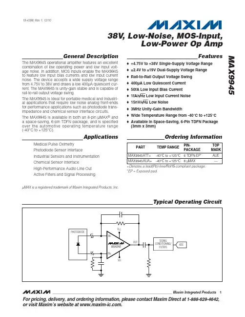
General DescriptionThe MAX9945 operational amplifier features an excellent combination of low operating power and low input volt-age noise. In addition, MOS inputs enable the MAX9945to feature low input bias currents and low input current noise. The device accepts a wide supply voltage range from 4.75V to 38V and draws a low 400µA quiescent cur-rent. The MAX9945 is unity-gain stable and is capable of rail-to-rail output voltage swing.The MAX9945 is ideal for portable medical and industri-al applications that require low noise analog front-ends for performance applications such as photodiode trans-impedance and chemical sensor interface circuits.The MAX9945 is available in both an 8-pin µMAX ®and a space-saving, 6-pin TDFN package, and is specified over the automotive operating temperature range (-40°C to +125°C).ApplicationsMedical Pulse Oximetry Photodiode Sensor InterfaceIndustrial Sensors and Instrumentation Chemical Sensor Interface High-Performance Audio Line Out Active Filters and Signal ProcessingFeatureso +4.75V to +38V Single-Supply Voltage Range o ±2.4V to ±19V Dual-Supply Voltage Range o Rail-to-Rail Output Voltage Swing o 400µA Low Quiescent Current o 50fA Low Input Bias Current o 1fA/√Hz Low Input Current Noise o 15nV/√Hz Low Noise o 3MHz Unity-Gain Bandwidtho Wide Temperature Range from -40°C to +125°C o Available in Space-Saving, 6-Pin TDFN Package (3mm x 3mm)MAX994538V , Low-Noise, MOS-Input,Low-Power Op Amp________________________________________________________________Maxim Integrated Products 119-4398; Rev 1; 12/10For pricing, delivery, and ordering information,please contact Maxim Direct at 1-888-629-4642,or visit Maxim’s website at .Ordering Information*EP = Exposed pad.µMAX is a registered trademark of Maxim Integrated Products, Inc.Typical Operating CircuitM A X 994538V , Low-Noise, MOS-Input,Low-Power Op AmpABSOLUTE MAXIMUM RATINGSELECTRICAL CHARACTERISTICSStresses beyond those listed under “Absolute Maximum Ratings” may cause permanent damage to the device. These are stress ratings only, and functional operation of the device at these or any other conditions beyond those indicated in the operational sections of the specifications is not implied. Exposure to absolute maximum rating conditions for extended periods may affect device reliability.Supply Voltage (V CC to V EE )..................................-0.3V to +40V IN+, IN-, OUT Voltage......................(V EE - 0.3V) to (V CC + 0.3V)IN+ to IN-.............................................................................±12V OUT Short Circuit to Ground Duration....................................10s Continuous Input Current into Any Pin.............................±20mA Continuous Power Dissipation (T A = +70°C)6-Pin TDFN-EP (derate 23.8mW/°C above +70°C)Multilayer Board....................................................1904.8mW8-Pin µMAX (derate 4.8mW/°C above +70°C)Multilayer Board......................................................387.8mW Operating Temperature Range .........................-40°C to +125°C Junction Temperature......................................................+150°C Storage Temperature Range.............................-65°C to +150°C Lead Temperature (soldering, 10s).................................+300°C Soldering Temperature....................................................+260°CNote 1:Package thermal resistances were obtained using the method described in JEDEC specification JESD51-7, using a four-layer board. For detailed information on package thermal considerations, refer to /thermal-tutorial .PACKAGE THERMAL CHARACTERISTICS (Note 1)TDFN-EPJunction-to-Ambient Thermal Resistance (θJA )............42°C/W Junction-to-Case Thermal Resistance (θJC )...................9°C/WµMAXJunction-to-Ambient Thermal Resistance (θJA ).......206.3°C/W Junction-to-Case Thermal Resistance θJC ...................42°C/WMAX994538V , Low-Noise, MOS-Input,Low-Power Op Amp_______________________________________________________________________________________3ELECTRICAL CHARACTERISTICS (continued)(V CC = +15V, V EE = -15V, V IN+= V IN-= V GND = 0V, R OUT = 100k Ωto GND, T A = -40°C to +125°C, typical values are at T A = +25°C,unless otherwise noted.) (Note 2)Note 3:Guaranteed by design. IN+ and IN- are internally connected to the gates of CMOS transistors. CMOS GATE leakage is sosmall that it is impractical to test in production. Devices are screened during production testing to eliminate defective units.Note 4:Specified over all temperatures and process variation by circuit simulation.M A X 994538V , Low-Noise, MOS-Input,Low-Power Op Amp 4_______________________________________________________________________________________Typical Operating Characteristics(V CC = +15V, V EE = -15V, V IN+= V IN-= V GND = 0V, R OUT = 100k Ωto GND, T A = -40°C to +125°C, typical values are at T A = +25°C,unless otherwise noted.)QUIESCENT SUPPLY CURRENTvs. SUPPLY VOLTAGE AND TEMPERATURESUPPLY VOLTAGE (V)S U P P L Y C U R R E N T (µA )3530252015103004005006002005OUTPUT VOLTAGE SWING LOWvs. TEMPERATURETEMPERATURE (°C)V O L - V E E (V )10012080604020-200.100.050.150.200.250-40OUTPUT VOLTAGE SWING HIGHvs. TEMPERATURETEMPERATURE (°C)V C C - V O H (V )10012080604020-200.100.050.150.200.250-40INPUT BIAS CURRENT vs. TEMPERATUREM A X 9945 t o c 04TEMPERATURE (°C)I B I A S (p A )10080602040-2001020304050607080-10-40120INPUT VOLTAGE 0.1Hz TO 10Hz NOISEMAX9945 toc051s/div 1µV/divINPUT VOLTAGE-NOISE DENSITYvs. FREQUENCYFREQUENCY (Hz)I N P U T V O L T A G E -N O I S E D E N S I T Y (n V H z )10,000100,0001000100101001000101TOTAL HARMONIC DISTORTIONvs. FREQUENCYFREQUENCY (Hz)T H D (d B )100,00010,0001000-90-70-80-110-100100TOTAL HARMONIC DISTORTION + NOISEvs. FREQUENCYFREQUENCY (Hz)T H D +N (d B )-90-80-70-60-50-100100,00010,000100100010INPUT OFFSET VOLTAGE vs. COMMON-MODE VOLTAGECOMMON-MODE VOLTAGE (V)I N P U T O F F S E T V O L T A G E (μV )105-10-510008000600400200-15MAX994538V , Low-Noise, MOS-Input,Low-Power Op Amp_______________________________________________________________________________________5INPUT OFFSET VOLTAGE vs. TEMPERATURETEMPERATURE (°C)I N P U T O F F S E T V O L T A G E (µV )100120804060-202010008000600400200-40OPEN-LOOP GAIN vs. FREQUENCYFREQUENCY (Hz)O P E N -L O O P G A I N (d B )12080-40401m1101001k10k 100k 1M 10MCOMMON-MODE REJECTION RATIOvs. FREQUENCYM A X 9945 t o c 12FREQUENCY (Hz)C M R R (d B )1M100k1001k10k-90-80-70-60-50-40-30-20-1001010MPOWER-SUPPLY REJECTION RATIOvs. FREQUENCYFREQUENCY (Hz)P S R R (d B )1M100k10k1k10010-100-80-60-40-200-120110MRESISTOR ISOLATION vs. CAPACITIVE LOADR ISO (Ω)C L O AD (p F )10010100010,0001001Typical Operating Characteristics (continued)(V CC = +15V, V EE = -15V, V IN+= V IN-= V GND = 0V, R OUT = 100k Ωto GND, T A = -40°C to +125°C, typical values are at T A = +25°C,unless otherwise noted.)M A X 994538V , Low-Noise, MOS-Input,Low-Power Op Amp 6_______________________________________________________________________________________Typical Operating Characteristics (continued)(V CC = +15V, V EE = -15V, V IN+= V IN-= V GND = 0V, R OUT = 100k Ωto GND, T A = -40°C to +125°C, typical values are at T A = +25°C,unless otherwise noted.)LARGE SIGNAL-STEP RESPONSE1μs/div +1V-1V V OUT 500mV/div SMALL SIGNAL-STEP RESPONSE2μs/div+20mV-20mVV OUT 10mV/divA V = 1V/V V IN = 40mV P-P R L = 100k ΩLARGE-SIGNAL RESPONSEvs. FREQUENCYFREQUENCY (kHz)O U T P U T V O L T A G E (V P -P )10,0001000100105101525203001LARGE SIGNAL-STEP RESPONSE4μs/div+5V-5VV OUT 2.5V/divOUTPUT IMPEDANCE vs. FREQUENCYFREQUENCY (Hz)O U T P U T I M P E D A N C E (Ω)1M100k10k1k1000.101.0010.00100.001000.000.011010MOP-AMP STABILITYvs. CAPACITIVE AND RESISTIVE LOADSPARALLEL LOAD RESISTANCE (k Ω)P A R A L L E L L O A D C A P A C I T A N C E (p F )10,0001001000100010010,0001010Detailed Description The MAX9945 features a combination of low input cur-rent and voltage noise, rail-to-rail output voltage swing, wide supply voltage range, and low-power operation. The MOS inputs on the MAX9945 make it ideal for use as transimpedance amplifiers and high-impedance sensor interface front-ends in medical and industrial applications. The MAX9945 can interface with small signals from either current-sources or high-output impedance voltage sources. Applications include pho-todiode pulse oximeters, pH sensors, capacitive pres-sure sensors, chemical analysis equipment, smoke detectors, and humidity sensors.A high 130dB open-loop gain (typ) and a wide supply voltage range, allow high signal-gain implementations prior to signal conditioning circuitry. Low quiescent supply current makes the MAX9945 compatible with portable systems and applications that operate under tight power budgets. The combination of excellent THD, low voltage noise, and MOS inputs also make the MAX9945 ideal for use in high-performance active fil-ters for data acquisition systems and audio equipment.Low-Current, Low-Noise Input Stage The MAX9945 features a MOS-input stage with only 50fA (typ) of input bias current and a low 1fA/√Hz(typ) input current-noise density. The low-frequency input voltage noise is a low 2µV P-P(typ). The input stage accepts a wide common-mode range, extending from the negative supply, V EE,to within 1.2V of the positive supply, V CC.The MAX9945 output stage swings to within 50mV (typ)of either power-supply rail with a 100kΩload and pro-vides a 3MHz GBW with a 2.2V/µs slew rate. The device is unity-gain stable, and unlike other deviceswith a low quiescent current, can drive a 120pF capaci-tive load without compromising stability.Applications InformationHigh-Impedance Sensor Front EndsHigh-impedance sensors can output signals of interestin either current or voltage form. The MAX9945 inter-faces to both current-output sensors such as photo-diodes and potentiostat sensors, and high-impedance voltage sources such as pH sensors.For current-output sensors, a transimpedance amplifieris the most noise-efficient method for converting theinput signal to a voltage. High-value feedback resistorsare commonly chosen to create large gains, while feed-back capacitors help stabilize the amplifier by cancel-ing any zeros in the transfer function created by ahighly capacitive sensor or cabling. A combination oflow-current noise and low-voltage noise is important forthese applications. Take care to calibrate out photodi-ode dark current if DC accuracy is important. The high bandwidth and slew rate also allows AC signal pro-cessing in certain medical photodiode sensor applica-tions such as pulse oximetry.MAX994538V, Low-Noise, MOS-Input,Low-Power Op Amp _______________________________________________________________________________________7Pin DescriptionM A X 9945F or voltage-output sensors, a noninverting amplifier is typically used to buffer and/or apply a small gain to, the input voltage signal. Due to the extremely high imped-ance of the sensor output, a low input bias current with a small temperature variation is very important for these applications.Power-Supply DecouplingThe MAX9945 operates from a +4.75V to +38V, V EE ref-erenced power supply. Bypass the power-supply inputs V CC and V EE to a quiet copper ground plane,with a 0.1µF ceramic capacitor in parallel with a 4.7µF electrolytic capacitor, placed close to the leads.Layout TechniquesA good layout is critical to obtaining high performance especially when interfacing with high-impedance sen-sors. Use shielding techniques to guard against para-sitic leakage paths. F or transimpedance applications,for example, surround the inverting input, and the traces connecting to it, with a buffered version of its own voltage. A convenient source of this voltage is the noninverting input pin. Pins 1, 5, and 8 on the µMAX package are unconnected, and can be connected to an analog common potential, or to the driven guard potential, to reduce leakage on the inverting input.A good layout guard rail isolates sensitive nodes, such as the inverting input of the MAX9945 and the traces connecting to it (see Figure 1), from varying or large volt-age differentials that otherwise occur in the rest of the circuit board. This reduces leakage and noise effects,allowing sensitive measurements to be made accurately.Take care to also decrease the amount of stray capaci-tance at the op amp’s inputs to improve stability. To achieve this, minimize trace lengths and resistor leads by placing external components as close as possible to the package. If the sensor is inherently capacitive, or is connected to the amplifier through a long cable, use a low-value feedback capacitor to control high-frequency gain and peaking to stabilize the feedback loop.38V , Low-Noise, MOS-Input,Low-Power Op Amp 8_______________________________________________________________________________________Figure 1. Shielding the Inverting Input to Reduce LeakageFigure 2. Input Differential Voltage ProtectionInput Differential Voltage ProtectionDuring normal op-amp operation, the inverting and non-inverting inputs of the MAX9945 are at approximately the same voltage. The ±12V absolute maximum input differential voltage rating offers sufficient protection for most applications. If there is a possibility of exceeding the input differential voltage specification, in the pres-ence of extremely fast input voltage transients or due to certain application-specific fault conditions, use exter-nal low-leakage pico-amp diodes and series resistors to protect the input stage of the amplifier (see Figure 2).The extremely low input bias current of the MAX9945allows a wide range of input series resistors to be used.If low input voltage noise is critical to the application,size the input series resistors appropriately.MAX994538V , Low-Noise, MOS-Input,Low-Power Op Amp_______________________________________________________________________________________9Chip InformationPROCESS: BiCMOSM A X 994538V , Low-Noise, MOS-Input,Low-Power Op Amp 10______________________________________________________________________________________Pin ConfigurationsMAX994538V , Low-Noise, MOS-Input,Low-Power Op AmpPackage InformationFor the latest package outline information and land patterns, go to /packages . Note that a “+”, “#”, or “-” in the package code indicates RoHS status only. Package drawings may show a different suffix character, but the drawing pertains to the package regardless of RoHS status.M A X 994538V , Low-Noise, MOS-Input,Low-Power Op Amp 12______________________________________________________________________________________MAX994538V , Low-Noise, MOS-Input,Low-Power Op Amp______________________________________________________________________________________13Package Information (continued)For the latest package outline information and land patterns, go to /packages . Note that a "+", "#", or "-" in the package code indicates RoHS status only. Package drawings may show a different suffix character, but the drawing pertains to the package regardless of RoHS status.M A X 994538V , Low-Noise, MOS-Input,Low-Power Op Amp Maxim cannot assume r esponsibility for use of any cir cuitr y other than cir cuitr y entir ely embodied in a Maxim pr oduct. No cir cuit patent licenses ar e implied. Maxim reserves the right to change the circuitry and specifications without notice at any time.14____________________Maxim Integrated Products, 120 San Gabriel Drive, Sunnyvale, CA 94086 408-737-7600©2010 Maxim Integrated ProductsMaxim is a registered trademark of Maxim Integrated Products, Inc.。