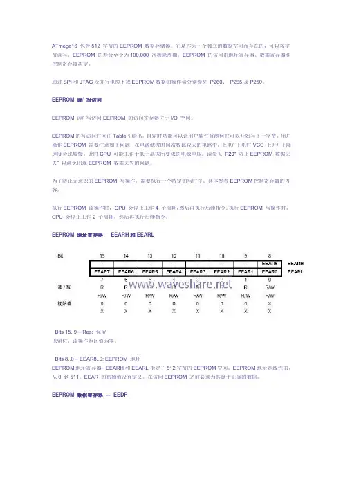
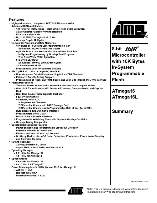
Features•High-performance, Low-power AVR® 8-bit Microcontroller •Advanced RISC Architecture–131 Powerful Instructions – Most Single-clock Cycle Execution –32 x 8 General Purpose Working Registers–Fully Static Operation–Up to 16 MIPS Throughput at 16 MHz–On-chip 2-cycle Multiplier•Nonvolatile Program and Data Memories–16K Bytes of In-System Self-Programmable FlashEndurance: 10,000 Write/Erase Cycles–Optional Boot Code Section with Independent Lock BitsIn-System Programming by On-chip Boot ProgramTrue Read-While-Write Operation–512 Bytes EEPROMEndurance: 100,000 Write/Erase Cycles–1K Byte Internal SRAM–Programming Lock for Software Security•JTAG (IEEE std. 1149.1 Compliant) Interface–Boundary-scan Capabilities According to the JTAG Standard–Extensive On-chip Debug Support–Programming of Flash, EEPROM, Fuses, and Lock Bits through the JTAG Interface •Peripheral Features–Two 8-bit Timer/Counters with Separate Prescalers and Compare Modes–One 16-bit Timer/Counter with Separate Prescaler, Compare Mode, and Capture Mode–Real Time Counter with Separate Oscillator–Four PWM Channels–8-channel, 10-bit ADC8 Single-ended Channels7 Differential Channels in TQFP Package Only2 Differential Channels with Programmable Gain at 1x, 10x, or 200x–Byte-oriented Two-wire Serial Interface–Programmable Serial USART–Master/Slave SPI Serial Interface–Programmable Watchdog Timer with Separate On-chip Oscillator–On-chip Analog Comparator•Special Microcontroller Features–Power-on Reset and Programmable Brown-out Detection–Internal Calibrated RC Oscillator–External and Internal Interrupt Sources–Six Sleep Modes: Idle, ADC Noise Reduction, Power-save, Power-down, Standby and Extended Standby•I/O and Packages–32 Programmable I/O Lines–40-pin PDIP, 44-lead TQFP, and 44-pad MLF•Operating Voltages–2.7 - 5.5V for ATmega16L–4.5 - 5.5V for ATmega16•Speed Grades–0 - 8 MHz for ATmega16L–0 - 16 MHz for ATmega16•Power Consumption @ 1 MHz, 3V, and 25°C for ATmega16L–Active: 1.1 mA–Idle Mode: 0.35 mA–Power-down Mode: < 1 µA 8-bit Microcontrollerwith 16K BytesNote: This is a summary document. A complete document is available on our Web site at .2ATmega16(L)2466HS–AVR–12/03Pin ConfigurationsFigure 1. Pinouts ATmega16DisclaimerTypical values contained in this datasheet are based on simulations and characteriza-tion of other AVR microcontrollers manufactured on the same process technology. Min and Max values will be available after the device is characterized.3ATmega16(L)2466HS–AVR–12/03OverviewThe ATmega16 is a low-power CMOS 8-bit microcontroller based on the AVR enhanced RISC architecture. By executing powerful instructions in a single clock cycle, the ATmega16 achieves throughputs approaching 1 MIPS per MHz allowing the system designer to optimize power consumption versus processing speed.Block DiagramFigure 2. Block Diagram4ATmega16(L)2466HS–AVR–12/03The AVR core combines a rich instruction set with 32 general purpose working registers.All the 32 registers are directly connected to the Arithmetic Logic Unit (ALU), allowing two independent registers to be accessed in one single instruction executed in one clock cycle. The resulting architecture is more code efficient while achieving throughputs up to ten times faster than conventional CISC microcontrollers.The ATmega16 provides the following features: 16K bytes of In-System Programmable Flash Program memory with Read-While-Write capabilities, 512 bytes EEPROM, 1K byte SRAM, 32 general purpose I/O lines, 32 general purpose working registers, a JTAG interface for Boundary-scan, On-chip Debugging support and programming, three flexible Timer/Counters with compare modes, Internal and External Interrupts, a serial programmable USART, a byte oriented Two-wire Serial Interface, an 8-channel, 10-bit ADC with optional differential input stage with programmable gain (TQFP package only),a programmable Watchdog Timer with Internal Oscillator, an SPI serial port, and six software selectable power saving modes. The Idle mode stops the CPU while allowing the USART, Two-wire interface, A/D Converter, SRAM, Timer/Counters, SPI port, and interrupt system to continue functioning. The Power-down mode saves the register con-tents but freezes the Oscillator, disabling all other chip functions until the next External Interrupt or Hardware Reset. In Power-save mode, the Asynchronous Timer continues to run, allowing the user to maintain a timer base while the rest of the device is sleeping.The ADC Noise Reduction mode stops the CPU and all I/O modules except Asynchro-nous Timer and ADC, to minimize switching noise during ADC conversions. In Standby mode, the crystal/resonator Oscillator is running while the rest of the device is sleeping.This allows very fast start-up combined with low-power consumption. In Extended Standby mode, both the main Oscillator and the Asynchronous Timer continue to run. The device is manufactured using Atmel’s high density nonvolatile memory technology.The On-chip ISP Flash allows the program memory to be reprogrammed in-system through an SPI serial interface, by a conventional nonvolatile memory programmer, or by an On-chip Boot program running on the AVR core. The boot program can use any interface to download the application program in the Application Flash memory. Soft-ware in the Boot Flash section will continue to run while the Application Flash section is updated, providing true Read-While-Write operation. By combining an 8-bit RISC CPU with In-System Self-Programmable Flash on a monolithic chip, the Atmel ATmega16 is a powerful microcontroller that provides a highly-flexible and cost-effective solution to many embedded control applications.The ATmega16 AVR is supported with a full suite of program and system development tools including: C compilers, macro assemblers, program debugger/simulators, in-circuit emulators, and evaluation kits.Pin DescriptionsVCC Digital supply voltage.GNDGround.Port A (PA7..PA0)Port A serves as the analog inputs to the A/D Converter.Port A also serves as an 8-bit bi-directional I/O port, if the A/D Converter is not used.Port pins can provide internal pull-up resistors (selected for each bit). The Port A output buffers have symmetrical drive characteristics with both high sink and source capability.When pins PA0 to PA7 are used as inputs and are externally pulled low, they will source current if the internal pull-up resistors are activated. The Port A pins are tri-stated when a reset condition becomes active, even if the clock is not running.5ATmega16(L)2466HS–AVR–12/03Port B (PB7..PB0)Port B is an 8-bit bi-directional I/O port with internal pull-up resistors (selected for each bit). The Port B output buffers have symmetrical drive characteristics with both high sink and source capability. As inputs, Port B pins that are externally pulled low will source current if the pull-up resistors are activated. The Port B pins are tri-stated when a reset condition becomes active, even if the clock is not running.Port B also serves the functions of various special features of the ATmega16 as listed on page 56.Port C (PC7..PC0)Port C is an 8-bit bi-directional I/O port with internal pull-up resistors (selected for each bit). The Port C output buffers have symmetrical drive characteristics with both high sink and source capability. As inputs, Port C pins that are externally pulled low will source current if the pull-up resistors are activated. The Port C pins are tri-stated when a reset condition becomes active, even if the clock is not running. If the JTAG interface is enabled, the pull-up resistors on pins PC5(TDI), PC3(TMS) and PC2(TCK) will be acti-vated even if a reset occurs.Port C also serves the functions of the JTAG interface and other special features of the ATmega16 as listed on page 59.Port D (PD7..PD0)Port D is an 8-bit bi-directional I/O port with internal pull-up resistors (selected for each bit). The Port D output buffers have symmetrical drive characteristics with both high sink and source capability. As inputs, Port D pins that are externally pulled low will source current if the pull-up resistors are activated. The Port D pins are tri-stated when a reset condition becomes active, even if the clock is not running.Port D also serves the functions of various special features of the ATmega16 as listed on page 61.RESETReset Input. A low level on this pin for longer than the minimum pulse length will gener-ate a reset, even if the clock is not running. The minimum pulse length is given in Table 15 on page 36. Shorter pulses are not guaranteed to generate a reset.XTAL1Input to the inverting Oscillator amplifier and input to the internal clock operating circuit.XTAL2Output from the inverting Oscillator amplifier.AVCCAVCC is the supply voltage pin for Port A and the A/D Converter. It should be externally connected to V CC , even if the ADC is not used. If the ADC is used, it should be con-nected to V CC through a low-pass filter.AREFAREF is the analog reference pin for the A/D Converter.6ATmega16(L)2466HS–AVR–12/03Register Summary7ATmega16(L)2466HS–AVR–12/03Notes:1.When the OCDEN Fuse is unprogrammed, the OSCCAL Register is always accessed on this address. Refer to the debug-ger specific documentation for details on how to use the OCDR Register.2.Refer to the USART description for details on how to access UBRRH and UCSRC.3.For compatibility with future devices, reserved bits should be written to zero if accessed. Reserved I/O memory addressesshould never be written.4.Some of the Status Flags are cleared by writing a logical one to them. Note that the CBI and SBI instructions will operate onall bits in the I/O Register, writing a one back into any flag read as set, thus clearing the flag. The CBI and SBI instructions work with registers $00 to $1F only.$01 ($21)TWSR TWS7TWS6TWS5TWS4TWS3–TWPS1TWPS0179$00 ($20)TWBRTwo-wire Serial Interface Bit Rate Register178AddressNameBit 7Bit 6Bit 5Bit 4Bit 3Bit 2Bit 1Bit 0Page8ATmega16(L)2466HS–AVR–12/03Instruction Set SummaryMnemonicsOperandsDescriptionOperationFlags#ClocksARITHMETIC AND LOGIC INSTRUCTIONSADD Rd, Rr Add two RegistersRd ← Rd + Rr Z,C,N,V,H 1ADC Rd, Rr Add with Carry two Registers Rd ← Rd + Rr + C Z,C,N,V,H 1ADIW Rdl,K Add Immediate to Word Rdh:Rdl ← Rdh:Rdl + K Z,C,N,V,S 2SUB Rd, Rr Subtract two RegistersRd ← Rd - Rr Z,C,N,V,H 1SUBI Rd, K Subtract Constant from Register Rd ← Rd - K Z,C,N,V,H 1SBC Rd, Rr Subtract with Carry two Registers Rd ← Rd - Rr - C Z,C,N,V,H 1SBCI Rd, K Subtract with Carry Constant from Reg.Rd ← Rd - K - C Z,C,N,V,H 1SBIW Rdl,K Subtract Immediate from Word Rdh:Rdl ← Rdh:Rdl - K Z,C,N,V,S 2AND Rd, Rr Logical AND RegistersRd ← Rd • Rr Z,N,V 1ANDI Rd, K Logical AND Register and Constant Rd ← Rd • K Z,N,V 1OR Rd, Rr Logical OR RegistersRd ← Rd v Rr Z,N,V 1ORI Rd, K Logical OR Register and Constant Rd ← Rd v K Z,N,V 1EOR Rd, Rr Exclusive OR Registers Rd ← Rd ⊕ Rr Z,N,V 1COM Rd One’s Complement Rd ← $FF − Rd Z,C,N,V 1NEG Rd Two’s Complement Rd ← $00 − Rd Z,C,N,V,H 1SBR Rd,K Set Bit(s) in Register Rd ← Rd v K Z,N,V 1CBR Rd,K Clear Bit(s) in Register Rd ← Rd • ($FF - K)Z,N,V 1INC Rd Increment Rd ← Rd + 1Z,N,V 1DEC Rd DecrementRd ← Rd − 1 Z,N,V 1TST Rd Test for Zero or Minus Rd ← Rd • Rd Z,N,V 1CLR Rd Clear Register Rd ← Rd ⊕ Rd Z,N,V 1SER Rd Set Register Rd ← $FF None 1MUL Rd, Rr Multiply Unsigned R1:R0 ← Rd x Rr Z,C 2MULS Rd, Rr Multiply SignedR1:R0 ← Rd x Rr Z,C 2MULSU Rd, Rr Multiply Signed with Unsigned R1:R0 ← Rd x Rr Z,C 2FMUL Rd, Rr Fractional Multiply Unsigned R1:R0 ← (Rd x Rr) << 1Z,C 2FMULS Rd, Rr Fractional Multiply SignedR1:R0 ← (Rd x Rr) << 1Z,C 2FMULSU Rd, Rr Fractional Multiply Signed with Unsigned R1:R0 ← (Rd x Rr) << 1Z,C 2BRANCH INSTRUCTIONSRJMP kRelative Jump PC ← PC + k + 1None 2IJMP Indirect Jump to (Z)PC ← ZNone 2JMP k Direct JumpPC ← kNone 3RCALL kRelative Subroutine Call PC ← PC + k + 1None 3ICALL Indirect Call to (Z)PC ← Z None 3CALL k Direct Subroutine Call PC ← kNone 4RET Subroutine Return PC ← STACK None 4RETI Interrupt Return PC ← STACKI 4CPSE Rd,Rr Compare, Skip if Equal if (Rd = Rr) PC ← PC + 2 or 3None 1 / 2 / 3CP Rd,Rr CompareRd − Rr Z, N,V,C,H 1 CPC Rd,Rr Compare with CarryRd − Rr − C Z, N,V,C,H 1CPI Rd,K Compare Register with Immediate Rd − KZ, N,V,C,H 1SBRC Rr, b Skip if Bit in Register Cleared if (Rr(b)=0) PC ← PC + 2 or 3 None 1 / 2 / 3SBRS Rr, b Skip if Bit in Register is Set if (Rr(b)=1) PC ← PC + 2 or 3None 1 / 2 / 3SBIC P, b Skip if Bit in I/O Register Cleared if (P(b)=0) PC ← PC + 2 or 3 None 1 / 2 / 3SBIS P, b Skip if Bit in I/O Register is Set if (P(b)=1) PC ← PC + 2 or 3None 1 / 2 / 3BRBS s, k Branch if Status Flag Set if (SREG(s) = 1) then PC ←PC+k + 1None 1 / 2BRBC s, k Branch if Status Flag Cleared if (SREG(s) = 0) then PC ←PC+k + 1None 1 / 2BREQ k Branch if Equal if (Z = 1) then PC ← PC + k + 1None 1 / 2BRNE k Branch if Not Equal if (Z = 0) then PC ← PC + k + 1None 1 / 2BRCS k Branch if Carry Set if (C = 1) then PC ← PC + k + 1None 1 / 2BRCC k Branch if Carry Cleared if (C = 0) then PC ← PC + k + 1None 1 / 2BRSH k Branch if Same or Higher if (C = 0) then PC ← PC + k + 1None 1 / 2BRLO k Branch if Lower if (C = 1) then PC ← PC + k + 1None 1 / 2BRMI k Branch if Minus if (N = 1) then PC ← PC + k + 1None 1 / 2BRPL k Branch if Plusif (N = 0) then PC ← PC + k + 1None 1 / 2BRGE k Branch if Greater or Equal, Signed if (N ⊕ V= 0) then PC ← PC + k + 1None 1 / 2BRLT k Branch if Less Than Zero, Signed if (N ⊕ V= 1) then PC ← PC + k + 1None 1 / 2BRHS k Branch if Half Carry Flag Set if (H = 1) then PC ← PC + k + 1None 1 / 2BRHC k Branch if Half Carry Flag Cleared if (H = 0) then PC ← PC + k + 1None 1 / 2BRTS k Branch if T Flag Set if (T = 1) then PC ← PC + k + 1None 1 / 2BRTC k Branch if T Flag Cleared if (T = 0) then PC ← PC + k + 1None 1 / 2BRVS k Branch if Overflow Flag is Set if (V = 1) then PC ← PC + k + 1None 1 / 2BRVCk Branch if Overflow Flag is Clearedif (V = 0) then PC ← PC + k + 1None1 / 29ATmega16(L)2466HS–AVR–12/03BRIE k Branch if Interrupt Enabled if ( I = 1) then PC ← PC + k + 1None 1 / 2BRID k Branch if Interrupt Disabled if ( I = 0) then PC ← PC + k + 1None 1 / 2DATA TRANSFER INSTRUCTIONSMOV Rd, Rr Move Between Registers Rd ← RrNone 1MOVW Rd, Rr Copy Register Word Rd+1:Rd ← Rr+1:RrNone 1LDI Rd, K Load Immediate Rd ← KNone 1LD Rd, X Load IndirectRd ← (X)None 2LD Rd, X+Load Indirect and Post-Inc.Rd ← (X), X ← X + 1None 2LD Rd, - X Load Indirect and Pre-Dec.X ← X - 1, Rd ← (X)None 2LD Rd, Y Load IndirectRd ← (Y)None 2LD Rd, Y+Load Indirect and Post-Inc.Rd ← (Y), Y ← Y + 1None 2LD Rd, - Y Load Indirect and Pre-Dec.Y ← Y - 1, Rd ← (Y)None 2LDD Rd,Y+q Load Indirect with Displacement Rd ← (Y + q)None 2LD Rd, Z Load IndirectRd ← (Z)None 2LD Rd, Z+Load Indirect and Post-Inc.Rd ← (Z), Z ← Z+1None 2LD Rd, -Z Load Indirect and Pre-Dec.Z ← Z - 1, Rd ← (Z)None 2LDD Rd, Z+q Load Indirect with Displacement Rd ← (Z + q)None 2LDS Rd, k Load Direct from SRAM Rd ← (k)None 2ST X, Rr Store Indirect(X) ← RrNone 2ST X+, Rr Store Indirect and Post-Inc.(X) ← Rr, X ← X + 1None 2ST - X, Rr Store Indirect and Pre-Dec.X ← X - 1, (X) ← Rr None 2ST Y, Rr Store Indirect(Y) ← RrNone 2ST Y+, Rr Store Indirect and Post-Inc.(Y) ← Rr, Y ← Y + 1None 2ST - Y, Rr Store Indirect and Pre-Dec.Y ← Y - 1, (Y) ← Rr None 2STD Y+q,Rr Store Indirect with Displacement (Y + q) ← Rr None 2ST Z, Rr Store Indirect(Z) ← RrNone 2ST Z+, Rr Store Indirect and Post-Inc.(Z) ← Rr, Z ← Z + 1None 2ST -Z, Rr Store Indirect and Pre-Dec.Z ← Z - 1, (Z) ← Rr None 2STD Z+q,Rr Store Indirect with Displacement (Z + q) ← Rr None 2STS k, RrStore Direct to SRAM (k) ← Rr None 2LPM Load Program Memory R0 ← (Z)None 3LPM Rd, Z Load Program MemoryRd ← (Z)None 3LPM Rd, Z+Load Program Memory and Post-Inc Rd ← (Z), Z ← Z+1None 3SPM Store Program Memory (Z) ← R1:R0None -IN Rd, P In Port Rd ← PNone 1OUT P, Rr Out PortP ← Rr None 1PUSH Rr Push Register on Stack STACK ← Rr None 2POP Rd Pop Register from Stack Rd ← STACKNone 2BIT AND BIT-TEST INSTRUCTIONSSBI P,b Set Bit in I/O Register I/O(P,b) ← 1None 2CBI P,b Clear Bit in I/O Register I/O(P,b) ← 0None 2LSL Rd Logical Shift Left Rd(n+1) ← Rd(n), Rd(0) ← 0Z,C,N,V 1LSR Rd Logical Shift Right Rd(n) ← Rd(n+1), Rd(7) ← 0Z,C,N,V 1ROL Rd Rotate Left Through Carry Rd(0)←C,Rd(n+1)← Rd(n),C ←Rd(7)Z,C,N,V 1ROR Rd Rotate Right Through Carry Rd(7)←C,Rd(n)← Rd(n+1),C ←Rd(0)Z,C,N,V 1ASR Rd Arithmetic Shift Right Rd(n) ← Rd(n+1), n=0..6Z,C,N,V 1SWAP Rd Swap Nibbles Rd(3..0)←Rd(7..4),Rd(7..4)←Rd(3..0)None 1BSET s Flag Set SREG(s) ← 1SREG(s)1BCLR s Flag ClearSREG(s) ← 0 SREG(s)1BST Rr, b Bit Store from Register to T T ← Rr(b)T 1BLD Rd, b Bit load from T to Register Rd(b) ← TNone 1SEC Set Carry C ← 1C 1CLC Clear Carry C ← 0C 1SEN Set Negative Flag N ← 1N 1CLN Clear Negative Flag N ← 0N 1SEZ Set Zero Flag Z ← 1Z 1CLZ Clear Zero Flag Z ← 0Z 1SEI Global Interrupt Enable I ← 1I 1CLI Global Interrupt Disable I ← 0I 1SES Set Signed Test Flag S ← 1S 1CLS Clear Signed Test FlagS ← 0S 1SEVSet Twos Complement Overflow.V ← 1V1CLVClear Twos Complement Overflow V ← 0 V1SET Set T in SREG T ← 1T 1CLT Clear T in SREG T ← 0 T 1SEH Set Half Carry Flag in SREG H ← 1H 1MnemonicsOperandsDescriptionOperationFlags#Clocks10ATmega16(L)2466HS–AVR–12/03CLHClear Half Carry Flag in SREG H ← 0H1MCU CONTROL INSTRUCTIONS NOP No Operation None 1SLEEP Sleep(see specific descr. for Sleep function)None 1WDR Watchdog Reset (see specific descr. for WDR/timer)None 1BREAKBreakFor On-Chip Debug OnlyNoneN/AMnemonics Operands DescriptionOperationFlags#Clocks11ATmega16(L)2466HS–AVR–12/0312ATmega16(L)2466HS–AVR–12/03Packaging Information44A13ATmega16(L)2466HS–AVR–12/0340P614ATmega16(L)2466HS–AVR–12/0344M115ATmega16(L)2466HS–AVR–12/03ErrataThe revision letter in this section refers to the revision of the ATmega16 device.ATmega16(L) Rev. I•IDCODE masks data from TDI input 1.IDCODE masks data from TDI inputThe JTAG instruction IDCODE is not working correctly. Data to succeeding devices are replaced by all-ones during Update-DR.Problem Fix / Workaround –If A Tmega16 is the only device in the scan chain, the problem is not visible.–Select the Device ID Register of the A Tmega16 by issuing the IDCODE instruction or by entering the T est-Logic-Reset state of the T AP controller to read out the contents of its Device ID Register and possibly data from succeeding devices of the scan chain. Issue the BYP ASS instruction to the ATmega16 while reading the Device ID Registers of preceding devices of the boundary scan chain.–If the Device IDs of all devices in the boundary scan chain must be captured simultaneously, the A Tmega16 must be the fist device in the chain.ATmega16(L) Rev. H•IDCODE masks data from TDI input 1.IDCODE masks data from TDI inputThe JTAG instruction IDCODE is not working correctly. Data to succeeding devices are replaced by all-ones during Update-DR.Problem Fix / Workaround –If A Tmega16 is the only device in the scan chain, the problem is not visible.–Select the Device ID Register of the A Tmega16 by issuing the IDCODE instruction or by entering the T est-Logic-Reset state of the T AP controller to read out the contents of its Device ID Register and possibly data from succeeding devices of the scan chain. Issue the BYP ASS instruction to the ATmega16 while reading the Device ID Registers of preceding devices of the boundary scan chain.–If the Device IDs of all devices in the boundary scan chain must be captured simultaneously, the A Tmega16 must be the fist device in the chain.ATmega16(L) Rev. G•IDCODE masks data from TDI input 1.IDCODE masks data from TDI inputThe JTAG instruction IDCODE is not working correctly. Data to succeeding devices are replaced by all-ones during Update-DR.Problem Fix / Workaround –If A Tmega16 is the only device in the scan chain, the problem is not visible.–Select the Device ID Register of the A Tmega16 by issuing the IDCODE instruction or by entering the T est-Logic-Reset state of the T AP controller to read out the contents of its Device ID Register and possibly data from succeeding devices of the scan chain. Issue the BYP ASS instruction to the ATmega16 while reading the Device ID Registers of preceding devices of the boundary scan chain.16ATmega16(L)2466HS–AVR–12/03–If the Device IDs of all devices in the boundary scan chain must be captured simultaneously, the A Tmega16 must be the fist device in the chain.17ATmega16(L)2466HS–AVR–12/03Datasheet Change Log for ATmega16This section contains a log on the changes made to the datasheet for ATmega16.Changes from Rev. 2466G-10/03 to Rev. 2466H-12/03All page numbers refer to this document.1.Updated “Calibrated Internal RC Oscillator” on page 27.Changes from Rev. 2466F-02/03 to Rev. 2466G-10/03All page numbers refer to this document.1.Removed “Preliminary” from the datasheet.2.Changed ICP to ICP1 in the datasheet.3.Updated “JTAG Interface and On-chip Debug System” on page 34.4.Updated assembly and C code examples in “Watchdog Timer Control Regis-ter – WDTCR” on page 41.5.Updated Figure 46 on page 101.6.Updated Table 15 on page 36, Table 82 on page 215 and Table 115 on page274.7.Updated “Test Access Port – TAP” on page 220 regarding JTAGEN.8.Updated description for the JTD bit on page 229.9.Added note 2 to Figure 126 on page 251.10.Added a note regarding JTAGEN fuse to Table 105 on page 259.11.Updated Absolute Maximum Ratings* and DC Characteristics in “ElectricalCharacteristics” on page 289.12.Updated “ATmega16 Typical Characteristics” on page 297.13.Fixed typo for 16 MHz MLF package in “Ordering Information” on page 11.14.Added a proposal for solving problems regarding the JTAG instructionIDCODE in “Errata” on page 15.Changes from Rev. 2466E-10/02 to Rev. 2466F-02/03All page numbers refer to this document.1.Added note about masking out unused bits when reading the ProgramCounter in “Stack Pointer” on page 10.2.Added Chip Erase as a first step in “Programming the Flash” on page 286 and“Programming the EEPROM” on page 287.3.Added the section “Unconnected pins” on page 53.18ATmega16(L)2466HS–AVR–12/034.Added tips on how to disable the OCD system in “On-chip Debug System” onpage 34.5.Removed reference to the “Multi-purpose Oscillator” application note and“32kHz Crystal Oscillator” application note, which do not exist.6.Added information about PWM symmetry for Timer0 and Timer2.7.Added note in “Filling the Temporary Buffer (Page Loading)” on page 252about writing to the EEPROM during an SPM Page Load.8.Removed ADHSM completely.9.Added Table 73, “TWI Bit Rate Prescaler,” on page 180 to describe the TWPSbits in the “TWI Status Register – TWSR” on page 179.10.Added section “Default Clock Source” on page 23.11.Added note about frequency variation when using an external clock. Noteadded in “External Clock” on page 29. An extra row and a note added in Table 118 on page 291. 12.Various minor TWI corrections.13.Added “Power Consumption” data in “Features” on page 1.14.Added section “EEPROM Write During Power-down Sleep Mode” on page 20.15.Added note about Differential Mode with Auto Triggering in “Prescaling andConversion Timing” on page 205.16.Added updated “Packaging Information” on page 12.Changes from Rev. 2466D-09/02 to Rev. 2466E-10/02All page numbers refer to this document.1.Updated “DC Characteristics” on page 289.Changes from Rev. 2466C-03/02 to Rev. 2466D-09/02All page numbers refer to this document.1.Changed all Flash write/erase cycles from 1,000 to 10,000.2.Updated the following tables: Table 4 on page 24, Table 15 on page 36, Table42 on page 83, Table 45 on page 110, Table 46 on page 110, Table 59 on page 141, Table 67 on page 165, Table 90 on page 233, Table 102 on page 257, “DC Characteristics” on page 289, Table 119 on page 291, Table 121 on page 293,and Table 122 on page 295.3.Updated “Errata” on page 15.Changes from Rev. 2466B-09/01 to Rev. 2466C-03/02All page numbers refer to this document.1.Updated typical EEPROM programming time, Table 1 on page 18.19ATmega16(L)2466HS–AVR–12/032.Updated typical start-up time in the following tables:Table 3 on page 23, Table 5 on page 25, Table 6 on page 26, Table 8 on page 27,Table 9 on page 27, and Table 10 on page 28.3.Updated Table 17 on page 41 with typical WDT Time-out.4.Added Some Preliminary Test Limits and Characterization Data.Removed some of the TBD's in the following tables and pages:Table 15 on page 36, Table 16 on page 40, Table 116 on page 272 (table removed in document review #D), “Electrical Characteristics” on page 289, Table 119 on page 291, Table 121 on page 293, and Table 122 on page 295.5.Updated TWI Chapter.Added the note at the end of the “Bit Rate Generator Unit” on page 176.6.Corrected description of ADSC bit in “ADC Control and Status Register A –ADCSRA” on page 217.7.Improved description on how to do a polarity check of the ADC doff results in“ADC Conversion Result” on page 214.8.Added JTAG version number for rev. H in Table 87 on page 227.9.Added not regarding OCDEN Fuse below Table 105 on page 259.10.Updated Programming Figures:Figure 127 on page 261 and Figure 136 on page 272 are updated to also reflect that AVCC must be connected during Programming mode. Figure 131 on page 268added to illustrate how to program the fuses.11.Added a note regarding usage of the “PROG_PAGELOAD ($6)” on page 278and “PROG_PAGEREAD ($7)” on page 278.12.Removed alternative algortihm for leaving JTAG Programming mode.See “Leaving Programming Mode” on page 286.13.Added Calibrated RC Oscillator characterization curves in section “ATmega16Typical Characteristics” on page 297.14.Corrected ordering code for MLF package (16MHz) in “Ordering Information”on page 11.15.Corrected Table 90, “Scan Signals for the Oscillators (1)(2)(3),” on page 233.Disclaimer: Atmel Corporation makes no warranty for the use of its products, other than those expressly contained in the Company’s standard warranty which is detailed in Atmel’s Terms and Conditions located on the Company’s web site. The Company assumes no responsibility for any errors which may appear in this document, reserves the right to change devices or specifications detailed herein at any time without notice, and does not make any commitment to update the information contained herein. No licenses to patents or other intellectual property of Atmel are granted by the Company in connection with the sale of Atmel products, expressly or by implication. Atmel’s products are not authorized for use as critical components in life support devices or systems.Atmel CorporationAtmel Operations2325 Orchard Parkway San Jose, CA 95131, USA Tel: 1(408) 441-0311Fax: 1(408) 487-2600Regional HeadquartersEuropeAtmel SarlRoute des Arsenaux 41Case Postale 80CH-1705 Fribourg SwitzerlandTel: (41) 26-426-5555Fax: (41) 26-426-5500AsiaRoom 1219Chinachem Golden Plaza 77 Mody Road Tsimshatsui East Kowloon Hong KongTel: (852) 2721-9778Fax: (852) 2722-1369Japan9F, Tonetsu Shinkawa Bldg.1-24-8 ShinkawaChuo-ku, Tokyo 104-0033JapanTel: (81) 3-3523-3551Fax: (81) 3-3523-7581Memory2325 Orchard Parkway San Jose, CA 95131, USA Tel: 1(408) 441-0311Fax: 1(408) 436-4314Microcontrollers2325 Orchard Parkway San Jose, CA 95131, USA Tel: 1(408) 441-0311Fax: 1(408) 436-4314La Chantrerie BP 7060244306 Nantes Cedex 3, France Tel: (33) 2-40-18-18-18Fax: (33) 2-40-18-19-60ASIC/ASSP/Smart CardsZone Industrielle13106 Rousset Cedex, France Tel: (33) 4-42-53-60-00Fax: (33) 4-42-53-60-011150 East Cheyenne Mtn. Blvd.Colorado Springs, CO 80906, USA Tel: 1(719) 576-3300Fax: 1(719) 540-1759Scottish Enterprise Technology Park Maxwell BuildingEast Kilbride G75 0QR, Scotland Tel: (44) 1355-803-000Fax: (44) 1355-242-743RF/AutomotiveTheresienstrasse 2Postfach 353574025 Heilbronn, Germany Tel: (49) 71-31-67-0Fax: (49) 71-31-67-23401150 East Cheyenne Mtn. Blvd.Colorado Springs, CO 80906, USA Tel: 1(719) 576-3300Fax: 1(719) 540-1759Biometrics/Imaging/Hi-Rel MPU/High Speed Converters/RF DatacomAvenue de Rochepleine BP 12338521 Saint-Egreve Cedex, France Tel: (33) 4-76-58-30-00Fax: (33) 4-76-58-34-80Literature Requests/literature2466HS–AVR–12/03© Atmel Corporation 2003. All rights reserved. Atmel ® and combinations thereof, AVR ®, and AVR Studio ® are the registered trademarks of Atmel Corporation or its subsidiaries. Microsoft ®, Windows ®, Windows NT ®, and Windows XP ® are the registered trademarks of Microsoft Corpo-ration. Other terms and product names may be the trademarks of others。