m2 revision
- 格式:ppt
- 大小:270.50 KB
- 文档页数:26

《英语》(新标准)(小学一起)五年级上册M2 教学设计Leading-in (8 mins)向学生出示活动1图片并提问:Tom and Sam both have a ball intheir hands but they feel different.But do you know why?引导并帮助学生学会说:heavy。
2. 请学生观看活动1动画,然后向学生展示spun sugar和shot的图片,请学生个体描述并反馈。
3. 播放活动1录音并请学生重复。
4. 告诉学生今天的任务。
今天我们要学习用合适的形容词来描述事物。
2. 观看活动1动画,思考并回答问题,尝试描述spun sugar和shot的图片。
3. 听音并重复。
境,初步理解heavy的词义。
通过介绍形容词的功能自然导入新课Step 3. Learningof the story (15 mins)1. 告诉学生:Today the children went to thesupermarket with Ms Smart. Howdid they describe the supermarketand the goods? Listen andunderline the key words andsentences.2. 播放录音,向学生展示课文的第二张图片并提出以下问题:①What’s the supermarket like?②What’s in the supermarket?请个别学生回答问题。
回答完第一个问题后,帮助学生总结并说出“What a big supermarket!”回答完第二个问题后,帮助学生完成PPT中的句子,请个别学生解释句子使用“There is” 和“Thereare”的原因。
1. 观看动画,仔细观察第二张图片,思考并回答问题。
2. 回答问题后尝试解释句子使用“There is” 和“There are”的原因。
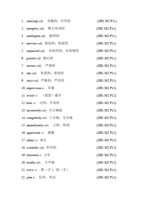
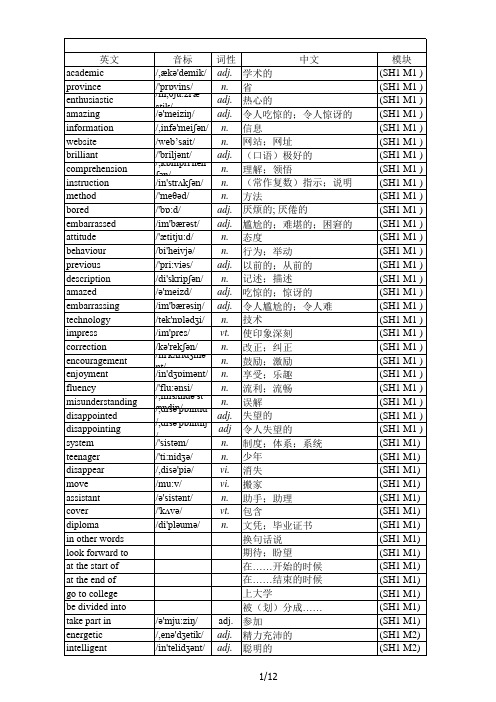
1.amusing adj.有趣的;可笑的(SH1 M2 P11)2.energetic adj.精力充沛的(SH1 M2 P11)3.intelligent adj.聪明的(SH1 M2 P11)4.nervous adj.紧张的;焦虑的(SH1 M2 P11)anised adj.有组织的;有系统的(SH1 M2 P11)6.patient adj.耐心的(SH1 M2 P11)7.serious adj.严肃的(SH1 M2 P11)8.shy adj.害羞的;羞怯的(SH1 M2 P11)9.strict adj.严格的;严厉的(SH1 M2 P11)10.impression n.印象(SH1 M2 P12)11.avoid vt.(故意)避开(SH1 M2 P12)12.hate vt. 讨厌;不喜欢(SH1 M2 P12)13.incorrectly adv. 不正确地(SH1 M2 P12)pletely adv.十分地;完全地(SH1 M2 P12)15.immediately adv.立即,即刻(SH1 M2 P12)16.appreciate vt.感激(SH1 M2 P12)17.admit vt.承认(SH1 M2 P12)18.scientific adj.科学的(SH1 M2 P12)19.literature n.文学(SH1 M2 P12)20.loudly adv.大声地(SH1 M2 P12)21.wave vt. 挥(手);招(手)(SH1 M2 P12)22.joke n.玩笑;笑话(SH1 M2 P12)23.summary n.总结;摘要;提要 (SH1 M2 P12)24.respect vt. & n.尊敬;尊重(SH1 M2 P12)25.grade n.(美)成绩;分数 (SH1 M2 P13)26.headmaster n.校长(SH1 M2 P15)27.headmistress n. 女校长(SH1 M2 P15)28.period n.一段时间(SH1 M2 P15)29.revision n.复习(SH1 M2 P15)30.translation n. 翻译(SH1 M2 P15)31.timetable n.时间表(SH1 M2 P15)32.topic n.话题;题目(SH1 M2 P15)33.vacation n.假期(SH1 M2 P15)34.revise vt.温习(功课)(SH1 M2 P17)35.discipline n.纪律(SH1 M2 P18)36.relationship n. 关系(SH1 M2 P19)37.formal adj.正式的(SH1 M2 P19)38.relaxed adj.轻松的;松懈的;宽松的(SH1 M2 P19)39.similarly adv.同样地,类似地(SH1 M2 P19)。

Teaching Plan for Oxford English 3A M2Unit 1 P4 RevisionTopic: A new friend—PeterTeaching Aids: multi-media, word cards, pictures, etc教学设计说明:期望通过本课时的复习,学会区别男女boy, girl; 并介绍周围人的体态身高特征fat, thin, tall, short;能在情景中进一步理解和运用He’s/ She’s…; Is he/she …?及Yes, he/she is./No, he/she isn’t.的表达;期望通过儿歌、游戏、对话等形式进一步巩固单元核心内容,通过自我介绍及介绍身边朋友等方式来增进相互间的了解,学会介绍沟通。
本课时教学目标:1.在情境中复习本单元核心单词,如:boy, girl, fat, thin, tall, short等,能辨别词形和含义;2.进一步了解字母e /e/的发音,学会判断,能举一反三;3.在情境中能进一步运用He’s/ She’s…; Is he/she …?及Yes, he/she is./No, he/she isn’t..等进行问答和交流;4.在情境中进一步增进相互间的了解,学会介绍沟通。
Material:I love my friends(Nobi and his friends are in Rainbow Primary School. Today Miss Fang introduces a new friend Peter to them.)Peter: Hello! My name is Peter. I’m a boy. I’m tall. I’m thin. I can ride a bicycle. I like riding.(Chatting in the classroom)Peter: Who’s your friend, Big G?Big G: She’s short. She’s thin. She’s eight. She can draw nice pictures.Peter: Is she Kitty?Big G: No, she isn’t.Peter: Is she Mina?Big G: Yes, she is. She is cute.Big G: Who’s your friend, Peter?Peter: My friend is eight.He’s short. He’s thin.Big G: Is he Sneech?Peter: No, he isn’t. He can run fast, but he can’t swim.Big G: Is he Nobi?Peter: Yes, he is. He is super.Listen and choose:1. Mina is thin.2. Peter is ten.3. Is Mina short? Yes, she is.4. Who’s your friend? My friend is Peter.5. Is she fat? No, she i sn’t.6. Who’s your good friend? My good friend is Peter.请自行设计作业单(包括:学习的材料、自我介绍的框架以及回家作业的清单---家长参与评价)(模仿上海市实验东校3AM2U1)。

Module 2单元备课教学重点难点:这个模块重点都在于学习如何表述及问答正在发生的动作。
1 、单词与词组:read running these picture taketake pictures children listen listen to talk talk to China2 、句型:She is reading a book.He’s taking pictures.She’s watching TV.He’s playing with a toy train.突破方法:A 、TPR 法学习词组,学唱P12 的歌曲来巩固。
B 、学习顺口溜:“我”用“am ”,“你”用“are ”,“is ”跟着“他、她、它”, 两个以上都用“are ”。
C 、直观演示帮助理解。
对于课文中出现的现在进行时这个语法内容,不要求教师讲解语法知识,更不要求学生掌握语法知识,在教学过程中,可以先通过直观的动作演示让学生充分理解ing 形式的意义,然后引导孩子们多说多造句,让他们从接受到慢慢习惯再到熟练使用该句型,最后达到在日常生活中自然运用的目的。
Unit 1 She’s reading a book.一、准备阶段:Ⅰ教学目标:情感目标:教育学生要尊敬父母知识目标:She’s …ing能力目标:能用“be doing”句型来描述正在发生的事情Ⅱ教学重点;1. 学习句型:be + ……ing2. 掌握单词及词组:read running these picture take take picturesⅢ教学难点:掌握由不发音”e”结尾单词加”ing”的规则Ⅳ辅助资源:挂图、录音机、磁带、图片二、教学过程:I. Warming up说chant.II. Revision:学生看图片轮流边做动作边说动词或词组III. Presentation:1.教师拿出一个照相机问学生:What’s this? 帮学生回答:“It’s a camera.” 教师说:“Yes, it’s my new camera.”同时做照相的动作。
Revision for 3A M2 U3 About meClass____________ Name_________________ No.________一、Read and recite 请熟读并拼背以下的单词、词组和句子Words单词about 关于(an) eye 眼睛(an) ear 耳朵nose 鼻子hair 头发(不可数名词) mouth 嘴巴Linda 琳达(人名) brown 棕色的little 小的;幼小的(an) animal动物rabbit 兔子tail 尾巴dog 狗mouse 老鼠mice 老鼠(复数) cat 猫green 绿色的Susie 苏西(人名) with 和…一起; 用pink 粉红色的ball 球pig 猪Jim 杰姆(人名) has 有(第三人称单数) his 他的stick 拐杖Phrases词组about me 关于我very short 非常矮/短little animals 小动物small and brown 小的和棕色的tall and fat 又高又胖play with 和…一起玩my pink ball 我的粉红色的球Sentences句子1. Hello, my name is Linda. I’m nine. I’m tall. I’m thin.My hair is long. My nose is small. My mouth is big. My eyes are big.And my ears are big too.2. Hello, I’m a boy. My hair is short, very short.Look at my eyes. My eyes are small and brown.My nose is big. My mouth is big too.Look. I’m tall and fat. Who am I? You are Danny. Yes, I’m Danny.3. Hello, I’m a rabbit. My eyes are red. My tail is short.Hello, I’m a dog. My ears are short. My nose is big.Hello, I’m a mouse. I’m thin. My eyes are small. My tail is long.Hello, I’m a cat. I’m fat. My eyes are big. My mouth is big too.4. Hello, I’m Susie. I’m a cat. I’m small and very fat.My tail is long. My ears are small. I like playing with my pink ball.5. Jim has a pig. His pig is big. His pig is pink. The big pig is playing with a stick.二、Learning tips 学习重点、难点、小贴士1. 学会认读音标:a cake t able Jane make platejam hand fat man has sad bade he she Peter Eva Chinese Japanese meten pen Ken red seveni kite bicycle like Mike nicepig pink Jim his is big playing with stick2. 学了这一单元, 你会用所学的句子介绍自己吗?根据下面的句型结构试一试, 写一写。
IGLOO2 M2GL050 (T , TS) Device ErrataER0200 v1.3 April 2016April 2016This Errata sheet contains information about known Errata specific to the IGLOO ®2 M2GL050 (T, TS) device family and provides available fixes and solutions.Table of ContentsRevision History . . . . . . . . . . . . . . . . . . . . . . . . . . . . . . . . . . . . . . . . . . . . . . . . . . . . . . . . . . . . . . . . . . .1Revisions Released per Device . . . . . . . . . . . . . . . . . . . . . . . . . . . . . . . . . . . . . . . . . . . . . . . . . . . . . . .1Errata for IGLOO2 M2GL050 (T, TS) All Temperature Grades . . . . . . . . . . . . . . . . . . . . . . . . . . . . . . .2Summary of IGLOO2 M2GL050 (T,TS) Device Errata . . . . . . . . . . . . . . . . . . . . . . . . . . . . . . . . . . . . .2Errata Descriptions and Solutions . . . . . . . . . . . . . . . . . . . . . . . . . . . . . . . . . . . . . . . . . . . . . . . . . . . . .3Usage Guidelines for IGLOO2 Devices . . . . . . . . . . . . . . . . . . . . . . . . . . . . . . . . . . . . . . . . . . . . . . . . .6Revision 0 and Revision 1 Devices . . . . . . . . . . . . . . . . . . . . . . . . . . . . . . . . . . . . . . . . . . . . . . . . . . . .6Revision 2 Device . . . . . . . . . . . . . . . . . . . . . . . . . . . . . . . . . . . . . . . . . . . . . . . . . . . . . . . . . . . . . . . . .6Product Support . . . . . . . . . . . . . . . . . . . . . . . . . . . . . . . . . . . . . . . . . . . . . . . . . . . . . . . . . . . . . . . . . . .7Table 1: Revision HistoryDate Version ChangesApril 2016 1.3Added Errata item 19.January 20161.2Updated Table 4 and Table 5: AutoProgramming and 2 Step IAP use SC_SPI programming interface.January 2016 1.1Added the following:•Information about Revision 2 of the M2GL050 device •Errata item 18.•Table 5June 20151.0Combined all M2GL050 (T,TS) device Errata.Table 2: Revisions Released per DeviceSilicon Devices Revisions Device Status M2GL050 (T, TS)All Temperature GradesProduction2IGLOO2 M2GL050 (T, TS) Device Errata ER0200 v1.3 April 2016Errata for IGLOO2 M2GL050 (T, TS) All Temperature GradesTable 3 lists the specific device Errata and the affected IGLOO2 M2GL050 (T, TS) revisions of all temperature grade devices .Table 3: Summary of IGLOO2 M2GL050 (T, TS) Device ErrataErrata No.ErrataSilicon Revisions M2GL050 (T, TS)Software ErrataRev (0, 1)Rev 21.MDDR and FDDR AXI interface does not support exclusive access X X –2.Apply DEVRST_N after ISP programmingX ––3.AXI wrap transfers with more than 32 bytes in burst mode are not supported for MDDR and FDDRX X –4.The MDDR/FDDR controller must be used with sequential burst mode with BL = 8 and PHY = 32, or PHY = 16X X –5.HPMS may reset when ENC_DATA_AUTHENTICATION or DEVICE_INFO STAPL commands are sentX ––6.VPP must be set to 2.5 V when programming/writing the eNVM at Industrial temperature rangeX ––7.Over-voltage support on MSIOs during Flash*Freeze mode X ––8.Verification of the FPGA fabric at junction temperatures higher than 50°C erroneously indicates a failureX ––9.DDR_OUT and I/O-Reg functional Errata due to a software bug ––X 10.Dedicated differential I/O driving the reference clock of the CCC may cause a functional failure due to a software bug––X 11.NVM Ready bit in eNVM Status register can generate a false READY signalX ––12.Power-up Digest is not supportedX ––13.Programming of the eNVM must only occur as part of a bitstream also containing the FPGA fabric––X 14.Updating eNVM from the FPGA fabric requires changes in the NV_FREQRNG registerX X –15.SYSCTRL_RESET_STATUS macro is not supported X X –16.Zeroization is not supportedX X –17.PCIe Hot Reset support requires a soft reset solutionX X –18.The DDR I/Os in M2GL050 (T, TS)-FG896 are non-compliant with the DDR3 standardX X –19.For S (security) grade devices, user must not enable write protection for Protected 4 K Regions, also known as Special Sectors in the eNVMXX–Note:Contact Microsemi SoC technical support , if you have additional questions. To order a specific die, contact your localMicrosemi sales office.IGLOO2 M2GL050 (T, TS) Device ErrataER0200 v1.3 April 20163Errata Descriptions and Solutions1.MDDR and FDDR AXI interface does not support exclusive accessThe MDDR and FDDR AXI interface in the M2GL050 device is compliant with AMBA AXI Protocol Specification v1.0, except for the exclusive access functionality. The future version of the Errata will have an updated information about the exclusive access functionality for the AXI interface.2.Apply DEVRST_N after ISP programmingM2GL050 devices support device programming in JTAG, Slave SPI, and ISP programming modes. However, after ISP programming, DEVRST_N needs to be asserted to reset the device or power cycle the device to run the new design.3.AXI wrap transfers with more than 32 bytes in burst mode are not supported for MDDR and FDDRDo not use wrap transfers with more than 32 bytes.4.The MDDR/FDDR controller must be used with sequential burst mode with BL = 8 and PHY = 32, or PHY = 16Though the MDDR and FDDR controllers in the M2GL050 devices support various burst modes/ lengths and PHY settings (as specified in the UG0446: SmartFusion2 and IGLOO2 FPGA High Speed DDR Interfaces User Guide), only a subset of these settings are supported.Recommendation:Only use sequential burst mode with BL = 8 for PHY16, or PHY32 modes for the MDDR or FDDR.5.HPMS may reset when ENC_DATA_AUTHENTICATION or DEVICE_INFO STAPL commands are sentThe HPMS resets after executing one of the following STAPL actions:•ENC_DATA_AUTHENTICATION •DEVICE_INFOAdditionally, if any of these actions are executed while a SmartDebug session is active, HPMS resets are observed.6.VPP must be set to 2.5 V when programming/writing the eNVM at Industrial temperature rangeVPP can be set to 2.5 V or 3.3 V. However, when writing or programming the eNVM of the M2GL050 devices below 0°C, VPP must be set to 2.5 V.Refer to the DS0128: IGLOO2 FPGA and SmartFusion2 SoC FPGA Datasheet for VPP minimum and maximum settings. Note that the eNVM reading with VPP set to 3.3 V or 2.5 V operates as intended.7.Over-voltage support on MSIOs during Flash*Freeze modeWhen the input voltage is driven above the reference voltage for that bank, additional current can be consumed in Flash*Freeze mode.4IGLOO2 M2GL050 (T, TS) Device Errata ER0200 v1.3 April 20168.Verification of the FPGA fabric at junction temperatures higher than 50°C erroneously indicates a failureStandalone verification (STAPL VERIFY action) must run at temperatures lower than 50°C. If aVERIFY action is run at temperatures higher than 50°C, a false verify failure may be reported. Note that the Check Digest system services can be used to confirm design integrity at temperatures within the recommended operation conditions.9.DDR_OUT and I/O-Reg functional Errata due to a software bugThis Errata is applicable only if you have created or updated the design using Libero ® SoC v11.1 SP1 or v11.1 SP2.The corresponding I/O does not function properly in the silicon due to the wrong software implementation of the I/O macro, if you have one of the following in the design:•If you use DDR_OUT macro in the design•If you combine an output or output enable register with an I/O using the PDC command set_io<portName> -register yesSolution:Both Errata are fixed in Libero SoC v11.1 SP3. Migrate the design to Libero SoC v11.1 SP3 or a newer version, and re-run Compile and Layout.10.Dedicated differential I/O driving the reference clock of the CCC may cause afunctional failure due to a software bugIf the design has a dedicated differential I/O pair driving the reference clock of the CCC, the input clock may not propagate to CCC due to a software bug and the device fails during silicon testing. There are several options to drive the ref clock of the CCC. One of the options is to drive from"Dedicated Input PAD x" (x = 0 to 3); this uses hardwired routing. In this option, choose single-ended I/O or differential I/O as the ref clock. This Errata exists when you choose the differential I/O option (dedicated differential I/O is used as CCC reference clock input).This Errata cannot be detected in any functional simulation, and can only be detected in silicon testing.Solution:The Errata is fixed in the Libero SoC 11.1 SP3. Migrate the design to Libero SoC 11.1 SP3 or newer version, and re-run Compile and Layout.11.NVM Ready bit in eNVM Status register can generate a false READY signalIf you send an instruction to the eNVM controller and then start polling the READY signal (bit0 of the eNVM Status register) to check when the eNVM controller is ready for the next function, the first assertion of the READY signal occurs when the eNVM controller is not yet ready, resulting in the generation of a false READY signal. However, the immediate next assertion of the READY signal correctly indicates that the eNVM controller is ready.Workaround:Add an extra eNVM Status bit read that polls/reads the eNVM Status bit twice as READY .12.Power-up Digest is not supportedWorkaround:Use NVM Data Integrity Check System service after the device is switched ON, and check the data integrity.IGLOO2 M2GL050 (T, TS) Device ErrataER0200 v1.3 April 2016513.Programming of the eNVM must only occur as part of a bitstream alsocontaining the FPGA fabricThe Bitstream Configuration Dialog Box in the Libero SoC allows the user to program eNVM and the FPGA fabric separately. However, for the current production of IGLOO2 FPGAs, the user needs to program the eNVM along with the FPGA fabric. The fabric can be programmed separately if needed.Solution:The Errata is fixed in the Libero SoC 11.1 SP3. Migrate the design to the Libero SoC 11.1 SP3 or newer version, and re-run Compile and Layout.14.Updating eNVM from the FPGA fabric requires changes in the NV_FREQRNGregisterWhen updating the eNVM from the FPGA fabric, NV_FREQRNG register must be changed from 0x07(default) to 0x0F, eNVM reads are not affected.15.SYSCTRL_RESET_STATUS macro is not supported 16.Zeroization is not supported17.PCIe Hot Reset support requires a soft reset solutionOn the IGLOO2 devices, a PCIe ® Hot Reset requires a soft FPGA logic reset scheme which clears the sticky bits of the PCI configuration space.Workaround:The application note AC437: Implementing PCIe Reset Sequence in SmartFusion2 and IGLOO2 Devices describes the PCIe Hot Reset reset scheme. However, this reset scheme causes PCIe violations in some cases.•At Gen1 rates, there are no violations.•At Gen2 rates, there are two PCIe CV violations.–Test case 1: TD_1_7 (Advanced Error Reporting Capability)–Test case 2: TD_1_41 (LinkCap2Control2Status2 Reg)18.The DDR I/Os in M2GL050 (T, TS)-FG896 are non-compliant with the DDR3standardThe DDR controller in the M2GL050-FG896 device is non-compliant with the DDR3 standard. Contact SoC tech support for additional information.19.For S (security) grade devices, user must not enable write protection forProtected 4 K Regions, also known as Special Sectors in the eNVMFor S (security) devices, there are two or four 4 KB regions per eNVM array that can be protected for read and write, these regions are known as Protected 4 K Regions or Special Sectors. If writeprotection is enabled for any of these regions, none of the locked pages inside the same eNVM block can be unlocked.6IGLOO2 M2GL050 (T, TS) Device Errata ER0200 v1.3 April 2016Usage Guidelines for IGLOO2 DevicesMicrosemi recommends the following conditions for the IGLOO2 device usage.1. Programming SupportThere may be package dependencies that may not expose certain programming interfaces. Refer to the DS0124: IGLOO2 Pin Descriptions Datasheet for device/package specific features.2. SHA-256 System ServiceMicrosemi recommends the message required to be on byte boundary when using SHA-256 System Service for the IGLOO2 devices.3. Accessing the PCIe Bridge Register in High-speed Serial InterfaceThe PCIe Bridge registers must not be accessed before the PHY is ready. Wait for the PHY_READY signal (which indicates when PHY is ready) to be asserted before updating the PCIe Bridge registers.The PHY_READY signal is normally asserted within 200 μs after the device is powered up. Wait for 200 μs before accessing the PCIe Bridge registers.Table 4: Revision 0 and Revision 1 DevicesProgramming Mode JTAG SPI Slave AutoProgramming Auto Update2 Step IAP Programming RecoveryProgramming Interface JTAG SC_SPI SC_SPI SPI_0SC_SPI SPI_0M2GL050 (T,TS)YesYesNoNoNoNoTable 5: Revision 2 DeviceProgramming Mode JTAG SPI Slave AutoProgramming Auto Update2 Step IAP Programming RecoveryProgramming Interface JTAG SC_SPI SC_SPI SPI_0SC_SPI SPI_0M2GL050 (T,TS)YesYesYesNoYesNoIGLOO2 M2GL050 (T, TS) Device ErrataER0200 v1.3 April 20167Product SupportMicrosemi SoC Products Group backs its products with various support services, including Customer Service, Customer Technical Support Center, a website, electronic mail, and worldwide sales offices. This appendix contains information about contacting Microsemi SoC Products Group and using these support services.Customer ServiceContact Customer Service for non-technical product support, such as product pricing, product upgrades, update information, order status, and authorization.From North America, call 800.262.1060From the rest of the world, call 650.318.4460Fax, from anywhere in the world 650. 318.8044Customer Technical Support CenterMicrosemi SoC Products Group staffs its Customer Technical Support Center with highly skilled engineers who can help answer your hardware, software, and design questions about Microsemi SoC Products. The Customer Technical Support Center spends a great deal of time creatingapplication notes, answers to common design cycle questions, documentation of known Errata and various FAQs. So, before you contact us, please visit our online resources. It is very likely we have already answered your questions.Technical SupportFor Microsemi SoC Products Support, visit/products/fpga-soc/design-support/fpga-soc-supportWebsiteYou can browse a variety of technical and non-technical information on the SoC home page , at /products/fpga-soc/fpga-and-soc .Contacting the Customer Technical Support CenterHighly skilled engineers staff the Technical Support Center. The Technical Support Center can be contacted by email or through the Microsemi SoC Products Group website.EmailYou can communicate your technical questions to our email address and receive answers back by email, fax, or phone. Also, if you have design problems, you can email your design files to receive assistance. We constantly monitor the email account throughout the day. When sending your request to us, please be sure to include your full name, company name, and your contact information for efficient processing of your request.The technical support email address is **********************.My CasesMicrosemi SoC Products Group customers may submit and track technical cases online by going to My Cases .Outside the U.S.Customers needing assistance outside the US time zones can either contact technical support via email(**********************) or contact a local sales office. Visit About Us for sales office listings and corporate contacts.8IGLOO2 M2GL050 (T, TS) Device Errata ER0200 v1.3 April 2016ITAR Technical SupportFor technical support on RH and RT FPGAs that are regulated by International Traffic in ArmsRegulations (ITAR), contact us via **********************. Alternatively, within My Cases, select Yes in the ITAR drop-down list. For a complete list of ITAR-regulated Microsemi FPGAs, visit the ITAR web page.Microsemi makes no warranty, representation, or guarantee regarding the information contained herein or the suitability of its products and services for any particular purpose, nor does Microsemi assume any liability whatsoever arising out of the application or use of any product or circuit. The products sold hereunder and any other products sold by Microsemi have been subject to limited testing and should not be used in conjunction with mission-critical equipment or applications. Any performance specifications are believed to be reliable but are not verified, and Buyer must conduct and complete all performance and other testing of the products, alone and together with, or installed in, any end-products. Buyer shall not rely on any data and performance specifications or parameters provided by Microsemi. It is the Buyer's responsibility to independently determine suitability of any products and to test and verify the same. The information provided by Microsemi hereunder is provided "as is, where is" and with all faults, and the entire risk associated with such information is entirely with the Buyer. Microsemi does not grant, explicitly or implicitly, to any party any patent rights, licenses, or any other IP rights, whether with regard to such information itself or anything described by such information. Information provided in this document is proprietary to Microsemi, and Microsemi reserves the right to make any changes to the information in this document or to any products and services at any time without notice.Microsemi Corporate Headquarters One Enterprise, Aliso Viejo,CA 92656 USAWithin the USA : +1 (800) 713-4113 Outside the USA : +1 (949) 380-6100Sales : +1 (949) 380-6136Fax : +1 (949) 215-4996E-mail: ***************************© 2016 Microsemi Corporation. All rights reserved. Microsemi and the Microsemi logo are trademarks of Microsemi Corporation. All other trademarks andservice marks are the property of their respective owners.Microsemi Corporation (Nasdaq: MSCC) offers a comprehensive portfolio of semiconductor and system solutions for communications, defense & security, aerospace and industrial markets. Products include high-performance and radiation-hardened analog mixed-signal integrated circuits, FPGAs, SoCs and ASICs; power management products; timing and synchronization devices and precise time solutions, setting the world’s standard for time; voice processing devices; RF solutions; discrete components; enterprise storage and communication solutions, security technologies and scalable anti-tamper products; Ethernet solutions; Power-over-Ethernet ICs and midspans; as well as custom design capabilities and services.Microsemi is headquartered in Aliso Viejo, Calif., and has approximately 4,800 employees globally. Learn more at .55900200-1.3/04.16。