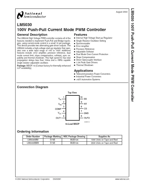
LM5030100V Push-Pull Current Mode PWM ControllerGeneral DescriptionThe LM5030High Voltage PWM controller contains all of the features needed to implement Push-Pull and Bridge topolo-gies,using current-mode control in a small 10pin package.This device provides two alternating gate driver outputs.The LM5030includes a high-voltage start-up regulator that oper-ates over a wide input range of 14V to 100V.Additional features include:error amplifier,precision reference,dual mode current limit,slope compensation,softstart,sync ca-pability and thermal shutdown.This high speed IC has total propagation delays less than 100ns and a 1MHz capable single resistor adjustable oscillator.Package:MSOP-10(Contact factory for thermally enhanced LLP availability).Featuresn Internal High Voltage Start-up Regulator n Single Resistor Oscillator Setting n Synchronizable n Error Amplifiern Precision Reference n Adjustable Softstartn Dual Mode Over-Current Protection n Slope Compensationn Direct Optocoupler Interface n 1.5A Peak Gate Drivers nThermal ShutdownApplicationsn Telecommunication Power Converters n Industrial Power Converters n +42V Automotive SystemsConnection DiagramTop View2005811210-Lead MSOPOrdering InformationOrder Number Package MarkingNSC Package DrawingSupplies AsLM5030MM S73B MUB10A 1000Units on Tape and Reel LM5030MMXS73BMUB10A3500Units on Tape and ReelAugust 2003LM5030100V Push-Pull Current Mode PWM Controller©2003National Semiconductor Corporation Block Diagram20058101FIGURE 1.L M 5030 2Pin DescriptionPin Name PinNumberDescription Application Information V IN1Source Input Voltage Input to start-up regulator.Input range14to100Volts.V FB2Inverting input to the error amplifier The non-inverting input is internally connected to a1.25Voltreference.COMP3Output to the error amplifier There is an internal5K resistor pull-up on this pin.The erroramplifier provides an active sink.Vcc4Output from the internal highvoltage series pass regulator.Theregulation setpoint is7.7Volts.If an auxiliary winding raises the voltage on this pin above the regulation setpoint the internal series pass regulator will shutdown,reducing the IC power dissipation.OUT15Output of the PWM controller Alternating PWM output gate driver.OUT26Output of the PWM controller Alternating PWM output gate driver.GND7Return GroundCS8Current sense input Current sense input for current mode control and current limiting separate dedicated comparators,if CS exceeds0.5Volt the outputs will go into Cycle by Cycle current limit.If CSexceeds0.625V the outputs will be disabled and a softstartcommenced.RT9Oscillator timing resistor pin andsynchronization input.An external resistor sets the oscillator frequency.This pin will also accept synchronization pulses from an external oscillator.SS10Dual purpose Softstart andShutdown pin A10µA current source and an external capacitor set the softstart timing length.The controller will enter a low power state if the SSpin is pulled below the typical shutdown threshold of0.45V.LM50303Absolute Maximum Ratings(Note 1)If Military/Aerospace specified devices are required,please contact the National Semiconductor Sales Office/Distributors for availability and specifications.V IN to GND (Survival)-0.3V to 100V V CC to GND (Survival)-0.3V to 16V RT to GND (Survival)-0.3V to 5.5V All other pins to GND (Survival)-0.3V to 7V Power Dissipation (Note 2)Internally LimitedESD Rating (Note 3)Human Body Model Machine Model2kV 200VLead Temperature(Soldering 4seconds)260˚CStorage Temperature Range -55˚C to +150˚CJunction Temperature150˚COperating RatingsJunction Temperature -40˚C to +105˚CV IN14V to 90VElectrical CharacteristicsSpecifications in standard type face are for T J =+25˚C and those in boldface type apply over the full operating junction tem-perature range.Unless otherwise specified:V IN =48V,V CC =10V,and RT =26.7K ΩSymbol ParameterConditionsMin (Note 4)Typ (Note 5)Max (Note 4)UnitsStartup Regulator V CC Reg V CC Regulation open ckt 7.47.78.0V V CC Current Limit(Note 2)1017mA I-V IN Startup Regulator Leakage (external Vcc Supply)V IN =90V150500µA I INShutdown CurrentSS =0V,V CC =open250350µAV CC SupplyV CC undervoltage Lockout VoltageVccReg -300mV VccReg -100mV V Undervoltage Hysteresis1.21.62.1V I CC Supply Current Cload =023mAError AmplifierGBWGain Bandwidth 4MHz DC Gain 75dB Input VoltageV FB =COMP1.220 1.245 1.270V COMP Sink CapabilityV FB =1.5V COMP=1V513mACurrent Limit CS1Cycle by Cycle CS Threshold Voltage0.450.50.55V CS2Restart CS Threshold Voltage Resets SS capacitor;auto restart0.5750.6250.675V ILIM Delay to OutputCS step from 0to 0.6V Time to onset of OUT Transition (90%)Cload =030nsCS Sink Current (clocked)CS =0.3V36mA Soft Start/ShutdownSoftstart Current Source 71013µA Softstart to COMP Offset 0.250.50.75V Shutdown Threshold0.20.450.7VL M 5030 4Electrical Characteristics(Continued)Specifications in standard type face are for T J=+25˚C and those in boldface type apply over the full operating junction tem-perature range.Unless otherwise specified:V IN=48V,V CC=10V,and RT=26.7KΩSymbol Parameter Conditions Min(Note4)Typ(Note5)Max(Note4)UnitsOscillatorFrequency1(RT=26.7K)175200225kHzFrequency2(RT=8.2K)510600690kHzSync threshold 3.2 3.8VPWM ComparatorDelay to Output COMP set to2V CSstepped0to0.4V,Timeto onset of OUT transitionlow30nsMax Duty Cycle Inferred from deadtime47.54950%Min Duty Cycle COMP=0V0%COMP to PWM ComparatorGain0.34COMP Open Circuit Voltage V FB=0V 4.3 5.2 6.1VCOMP Short Circuit Current V FB=0V,COMP=0V0.6 1.1 1.5mASlope CompensationSlope Comp Amplitude Delta increase at PWMComparator to CS80105130mVOutput SectionDeadtime Cload=0,10%to10%85135185nsOutput High Saturation Iout=50mA,V CC-V OUT0.250.75VOutput Low Saturation I OUT=100mA0.250.75VRise Time Cload=1nF16nsFall Time Cload=1nF16nsThermal ShutdownTsd Thermal Shutdown Temp.165˚C Thermal Shutdown Hysteresis15˚C Note1:Absolute Maximum Ratings are limits beyond which damage to the device may occur.Operating Ratings are conditions under which operation of the device is intended to be functional.For guaranteed specifications and test conditions,see the Electrical Characteristics.Note2:The maximum allowable power dissipation is a function of the maximum junction temperature,T J(MAX),the junction-to-ambient thermal resistance,θJA,and the ambient temperature,T A.The maximum allowable power dissipation at any ambient temperture is calculated using:Where the value ofθJA for the mini SO-10(MM)package is200˚C/W.Exceeding the maximum allowable dissipation will cause excessive die temperature,and the device will go into thermal shutdown.Note3:The human body model is a100pF capacitor discharged through a1.5kΩresistor into each pin.The machine model is a200pF capacitor discharged directly into each pin.The machine model ESD rating for pin5and pin6is150V.Note4:Limits are100%production tested at25˚C.Limits over the operating temperature range are guaranteed through correlation using Statistical Quality Control (SQC)methods.The limits are used to calculate National’s Average Outgoing Quality Level(AOQL).Note5:Typical numbers represent the most likely parametric norm for25˚C operation.LM50305Typical Performance CharacteristicsUnless otherwise specified:T J =25˚C.V CC vs V INV CC vs I CC (V IN =48V)2005810520058107Oscillator Frequency vs RTOscillator Frequency vs TemperatureRT =26.7k Ω2005810820058109Soft Start Current vs Temperature Deadtime vs Temperature2005811020058111L M 5030 6Typical Performance Characteristics Unless otherwise specified:TJ=25˚C.(Continued) Feedback Amplifier Gainphase20058115Detailed Operating DescriptionThe LM5030High Voltage PWM controller contains all of the features needed to implement Push-Pull and Bridge topolo-gies,using current-mode control in a small10pin package. Features included are,startup regulator,dual mode current limit,dual alternating gate drivers,thermal shutdown,soft-start and slope compensation.This high speed IC has total propagation delays<100nS.The Functional Block Diagram of the LM5030is shown in Figure1.The LM5030is designed for Current-Mode Control convert-ers which require alternating outputs,such as Push-Pull and Half/Full Bridge topologies.The features included in the LM5030enable all of the advantages of Current-Mode Con-trol,line feed-forward,cycle by cycle current limit and sim-plified loop compensation.The oscillator ramp is internally buffered and added to the PWM comparator input to provide slope compensation necessary for current mode control at higher duty cycles.High Voltage Start-Up RegulatorThe LM5030contains an internal high voltage startup regu-lator.The input pin(Vin)can be connected directly to line voltages as high as100V.The regulator output is internally current limited to10mA.Upon power up,the regulator is enabled and sources current into an external capacitor con-nected to the V CC pin.The recommended capacitance range for the V CC regulator is0.1µF to50µF.When the voltage on the V CC pin reaches the regulation point of7.7V,the control-ler outputs are enabled.The outputs will remain enabled unless,V CC falls below6.1V or if the SS/SHUTDOWN pin is pulled to ground or an over temperature condition occurs.In typical applications,an auxiliary transformer winding is diode connected to the V CC pin.This winding raises the V CC voltage greater than8V,effectively shutting off the internal startup regulator and saving power while reducing the con-troller dissipation.The external V CC capacitor must be sized such that the self-bias will maintain a V CC voltage greater than6.1V during the initial start-up.During a fault mode when the converter self bias winding is inactive,external current draw on the V CC line should be limited as to not exceed the maximum power dissipation of the controller.An external start-up or other bias rail can be used instead of the internal start-up regulator by connecting the V CC and the Vin pins and feeding the external bias voltage(8-15V)to that node.Error AmplifierAn internal high gain error amplifier is provided within theLM5030.The amplifier’s non-inverting reference is tied to1.25V.In non-isolated applications the power converter out-put is connected to the VFB pin via the voltage settingresistors and loop compensation is connected between theCOMP and VFB pins.For most isolated applications the error amplifier function isimplemented on the secondary side ground.Since the inter-nal error amplifier is configured as an open drain output itcan be disabled by connecting VFB to ground.The internal5K pull-up resistor,connected between the5V reference andCOMP,can be used as the pull-up for an optocoupler orother isolation device.PWM ComparatorThe PWM comparator compares the compensated currentramp signal to the loop error voltage from the internal erroramplifier(COMP pin).This comparator is optimized forspeed in order to achieve minimum discernable duty cycles.The comparator polarity is such that zero Volts on the COMPpin will cause a zero duty cycle.Current Limit/Current SenseThe LM5030contains two levels of over-current protection.Ifthe voltage on the current sense comparator exceeds0.5Volts the present cycle is terminated(cycle by cycle currentlimit).If the voltage on the current sense comparator ex-ceeds0.625Volts,the controller will terminate the presentcycle and discharge the softstart capacitor.A small RC filter,located near the controller,is recommended for the CS pin.An internal MOSFET discharges the current sense filtercapacitor at the conclusion of every cycle,to improve dy-namic performance.The LM5030CS and PWM comparators are very fast,andas such will respond to short duration noise youtconsiderations are critical for the current sense filter andsense resistor.The capacitor associated with the CS filtermust be placed very close to the device and connecteddirectly to the pins of the IC(CS and RTN).Also if a currentsense transformer is used,both leads of the transformersecondary should be routed to the sense resistor,whichshould also be located close to the IC.If a current senseresistor located in the drive transistor sources is used,forcurrent sense,a low inductance resistor should be chosen.LM50307Current Limit/Current Sense(Continued)In this case all of the noise sensitive low power grounds should be commoned together around the IC and then a single connection should be made to the power ground (sense resistor ground point).The second level threshold is intended to protect the power converter by initiating a low duty cycle hiccup mode when abnormally high,fast rising currents occur.During excessive loading,the first level threshold will always be reached and the output characteristic of the converter will be that of a current source but this sustained current level can cause excessive temperatures in the power train especially the output rectifiers.If the second level threshold is reached,the softstart capacitor will be fully discharged,a retry will com-mence following the discharge detection.The second level threshold will only be reached when a high dV/dt is present at the current sense pin.The signal must be fast enough to reach the second level threshold before the first threshold detector turns off the driver.This can usually happen for a saturated power inductor or shorted load.Excessive filtering on the CS pin,extremely low value current sense resistor or an inductor that does not saturate with excessive loading may prevent the second level threshold from ever being reached.Oscillator,Shutdown and Sync CapabilityThe LM5030oscillator is set by a single external resistor connected between the RT pin and return.To set a desired oscillator frequency the necessary RT resistor can be calcu-lated as:Each output switches at half the oscillator frequency in a Push-Pull configuration.The LM5030can also be synchro-nized to an external clock.The external clock must be of higher frequency than the free running frequency set by the RT resistor.The clock signal should be capacitively coupled into the RT pin with a 100pF capacitor.A peak voltage level greater than 3Volts with respect to ground is required for detection of the sync pulse.The sync pulse width should be set in the 15to 150nS range by the external components.The RT resistor is always required,whether the oscillator is free running or externally synchronized.The voltage at the RT pin is internally regulated to a nominal 2Volts.The RT resistor should be located very close to the device and connected directly to the pins of the IC (RT and GND).Slope CompensationThe PWM comparator compares the current sense signal to the voltage derived from the COMP pin.The COMP voltage is set by either the internal error amplifier or an external error amplifier through an optocoupler.At duty cycles greater than 50%(composite of alternating outputs)current mode control circuits are prone to subharmonic oscillation.By adding an additional ramp signal to the current sense ramp signal this condition can be avoided.The LM5030integrates this slope compensation by buffering the internal oscillator ramp and summing it internally to the current sense (CS)signal.Addi-tional slope compensation may be added by increasing the source impedance of the current sense signal.Soft Start/ShutdownThe softstart feature allows the converter to gradually reach the initial steady state operating point,thus reducing start-up stresses and surges.An internal 10uA current source and an external capacitor generate a ramping voltage signal which limits the error amplifier output during start-up.In the event of a second level current limit fault,the softstart capacitor will be fully discharged which disables the output drivers.When the fault condition is no longer present,the softstart capaci-tor is released to ramp and gradually restart the converter.The SS pin can also be used to disable the controller.If the SS pin voltage is pulled down below 0.45V (nominal)the controller will disable the outputs and enter a low power state.OUT1,OUT2and Time DelayThe LM5030provides two alternating outputs,OUT1and OUT2.The internal gate drivers can each sink 1.5A peak each.The maximum duty cycle for each output is inherently limited to less than 50%.The typical deadtime between the falling edge of one gate driver output and the rising edge of the other gate driver output is 135ns.Thermal ProtectionInternal Thermal Shutdown circuitry is provided to protect the integrated circuit in the event the excessive junction tem-perature.When activated,typically at 165degrees Celsius,the controller is forced into a low power reset state,disabling the output drivers and the bias regulator.This feature is provided to prevent catastrophic failures from accidental device overheating.L M 5030 8T y p i c a l A p p l i c a t i o n C i r c u i tT y p i c a l A p p l i c a t i o n C i r c u i t ,36V -75V I N a n d 3.3V ,10A O U T20058103LM50309ITEM PART NUMBERDESCRIPTIONVALUE C 1C0805C472K5RAC Capacitor,CER,KEMET 4700p,50V C 2C0805C103K5RAC Capacitor,CER,KEMET 0.01µ,50V C 3C4532X7S0G686M Capacitor,CER,TDK 68µ,4V C 4T520D337M006AS4350Capacitor,TANT,KEMET 330µ,6.3V C 5T520D337M006AS4350Capacitor,TANT,KEMET 330µ,6.3V C 6C4532X7R3A103K Capacitor,CER,TDK 0.01µ,1000V C 7C3216X7R2A104K Capacitor,CER,TDK 0.1µ,100V C 8C4532X7R2A105M Capacitor,CER,TDK 1µ,100V C 9C4532X7R2A105M Capacitor,CER,TDK 1µ,100V C 10C0805C102K1RAC Capacitor,CER,KEMET 1000p,100V C 11C1206C223K5RAC Capacitor,CER,KEMET 0.022µ,50V C 12C3216X7R1E105M Capacitor,CER,TDK 1µ,25V C 13C3216COG2J221J Capacitor,CER,TDK 220p,630V C 14C3216COG2J221J Capacitor,CER,TDK 220p,630V C 15C1206C104K5RAC Capacitor,CER,KEMET 0.1µ,50V C 16C0805C101J1GAC Capacitor,CER,KEMET 100p,100V C 17C0805C101J1GAC Capacitor,CER,KEMET 100p,100V C 18C3216X7R1H334K Capacitor,CER,TDK 0.33µ,50µD 1MBRB3030CTL Diode,Schottky,ON D 2CMPD2838-NSA Diode,Signal,Central D 3CMPD2838-NSA Diode,Signal,Central D 4CMPD2838-NSA Diode,Signal,Central D 5CMPD2838-NSA Diode,Signal,Central L 1MSS6132-103Input Choke,Coilcraft 10µH,1.5A L 2A9785-BOutput Choke,Coilcraft 7µH R 1CRCW12061R00F Resistor 1R 2CRCW12064990F Resistor 499R 3CRCW2512101J Resistor 100,1W R 4CRCW2512101J Resistor 100,1W R 5CRCW12064022F Resistor 40.2K R 6CRCW120610R0F Resistor 10R 7CRCW120610R0F Resistor 10R 8CRCW12061002F Resistor 10K R 9CRCW120623R7F Resistor 23.7R 10CRCW12062002F Resistor 20K R 11CRCW120610R0F Resistor 10R 12CRCW12063010F Resistor 301R 13CRCW120610R0F Resistor 10R 14CRCW12061001F Resistor1KTX 1A9784-B POWER XFR,COILCRAFT TX 2P8208T CURRENT XFR,Pulse 100:1U11LM5030REGULATOR,NATIONAL U22MOCD207M OPTO-COUPLER,QT OPTOELECTRONICS U33LM3411AM5-3.3REFERENCE,NATIONAL 651-1727010DUAL TERMINALS,MOUSER 3per ASSY X 1SUD19N20-90FET,N,200V,SILICONIX X2SUD19N20-90FET,N,200V,SILICONIXL M 5030 10Physical Dimensionsinches (millimeters)unless otherwise noted10Lead MSOP Package NS Package Number MUB10ALIFE SUPPORT POLICYNATIONAL’S PRODUCTS ARE NOT AUTHORIZED FOR USE AS CRITICAL COMPONENTS IN LIFE SUPPORT DEVICES OR SYSTEMS WITHOUT THE EXPRESS WRITTEN APPROVAL OF THE PRESIDENT AND GENERAL COUNSEL OF NATIONAL SEMICONDUCTOR CORPORATION.As used herein:1.Life support devices or systems are devices or systems which,(a)are intended for surgical implant into the body,or (b)support or sustain life,and whose failure to perform when properly used in accordance with instructions for use provided in the labeling,can be reasonably expected to result in a significant injury to the user.2.A critical component is any component of a life support device or system whose failure to perform can be reasonably expected to cause the failure of the life support device or system,or to affect its safety or effectiveness.National Semiconductor Americas Customer Support CenterEmail:new.feedback@ Tel:1-800-272-9959National SemiconductorEurope Customer Support CenterFax:+49(0)180-5308586Email:europe.support@Deutsch Tel:+49(0)6995086208English Tel:+44(0)8702402171Français Tel:+33(0)141918790National Semiconductor Asia Pacific Customer Support CenterEmail:ap.support@National SemiconductorJapan Customer Support Center Fax:81-3-5639-7507Email:jpn.feedback@ Tel:81-3-5639-7560LM5030100V Push-Pull Current Mode PWM ControllerNational does not assume any responsibility for use of any circuitry described,no circuit patent licenses are implied and National reserves the right at any time without notice to change said circuitry and specifications.元器件交易网。

![adc0808中文资料[整理版]](https://imgs-1438308264.cos.ap-hongkong.myqcloud.com/c09ee7f85ff7ba0d4a7302768e9951e79b896975.webp)