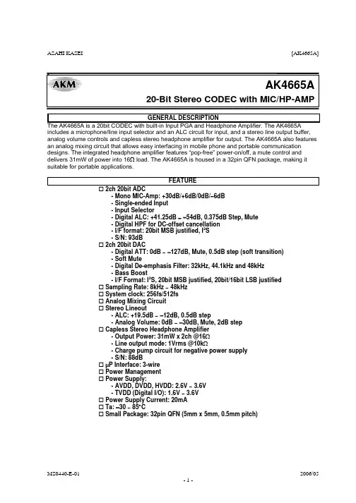
元器件交易网ASAHI KASEI[AK4665A]-AK4665A20-Bit Stereo CODEC with MIC/HP-AMPGENERAL DESCRIPTION The AK4665A is a 20bit CODEC with built-in Input PGA and Headphone Amplifier. The AK4665A includes a microphone/line input selector and an ALC circuit for input, and a stereo line output buffer, analog volume controls and capless stereo headphone amplifier for output. The AK4665A also features an analog mixing circuit that allows easy interfacing in mobile phone and portable communication designs. The integrated headphone amplifier features “pop-free” power-on/off, a mute control and delivers 31mW of power into 16Ω load. The AK4665A is housed in a 32pin QFN package, making it suitable for portable applications. FEATURE 2ch 20bit ADC - Mono MIC-Amp: +30dB/+6dB/0dB/−6dB - Single-ended Input - Input Selector - Digital ALC: +41.25dB ∼ −54dB, 0.375dB Step, Mute - Digital HPF for DC-offset cancellation - I/F format: 20bit MSB justified, I2S - S/N: 93dB 2ch 20bit DAC - Digital ATT: 0dB ∼ −127dB, Mute, 0.5dB step (soft transition) - Soft Mute - Digital De-emphasis Filter: 32kHz, 44.1kHz and 48kHz - Bass Boost - I/F Format: I2S, 20bit MSB justified, 20bit/16bit LSB justified Sampling Rate: 8kHz ∼ 48kHz System clock: 256fs/512fs Analog Mixing Circuit Stereo Lineout - ALC: +19.5dB ∼ −12dB, 0.5dB step - Analog Volume: 0dB ∼ −30dB, Mute, 2dB step Capless Stereo Headphone Amplifier - Output Power: 31mW x 2ch @16Ω - Line output mode: 1Vrms @10kΩ - Charge pump circuit for negative power supply - S/N: 88dB µP Interface: 3-wire Power Management Power Supply: - AVDD, DVDD, HVDD: 2.6V ∼ 3.6V - TVDD (Digital I/O): 1.6V ∼ 3.6V Power Supply Current: 20mA Ta: −30 ∼ 85°C Small Package: 32pin QFN (5mm x 5mm, 0.5mm pitch)MS0440-E-01 -1-2006/05元器件交易网ASAHI KASEI[AK4665A]AVDDPMMPAVSSVREFVCOMDVDD DVSSTVDDMPWRMIC PowerVREFVCOMPMVCMPMADCMICINMIC-AmpAINL1 ADC AINR1 Audio I/F Controller MCLK HPF ALC1 BICK LRCK SDTO HP-Amp DACPMHPRPMHPLPMDACHPL DATT DEM SMUTE BoostSDTIHPRLOUT ATT ROUTPMLOControl ALC2 RegisterCSN CCLK CDTIPDN LIN RIN MIN LPF LPF LPFPMCP PMHPL or PMHPR or PMLOHVDD HVSS Charge PumpCPCNNVSSFigure 1. Block DiagramMS0440-E-01 -2-2006/05元器件交易网ASAHI KASEI[AK4665A]Ordering GuideAK4665AEN AKD4665A 32pin QFN (0.5mm pitch) −30 ∼ +85°C Evaluation board for AK4665APin LayoutMPWRAINR1MICINAINL1182423222120AVSS AVDD VCOM VREF PDN CSN CCLK CDTI1917LOUTMINRINLIN25 26 27 28 29 30 31 32 1 2 3 4 5 6 7 816 15 14ROUT HPR HPL NVSS HVSS HVDD CN CPAK4665AENTop View13 12 11 10 9Comparison Table between AK4569 and AK4665AFunction HP-Amp Power Supply HP-Amp Output MIC-Amp MIC-Power ALC for Recording ALC for Playback Loopback SDTO Disable Lineout MCLK Power Supply Package AK4569 Single Power Supply 8.7mW@16Ω No No Analog MIC: +32 ∼ −19dB, 0.5dB step LINE: +20 ∼ −31dB, 0.5dB step No No No Mono CMOS or AC coupling input 2.5 ∼ 3.6V 28QFN (5.2mm x 5.2mm, 0.5mm pitch) AK4665A Dual Power Supply (Single Power Supply as external case) 31mW@16Ω Yes Yes Digital +41.25 ∼ −54dB, 0.375dB step Yes Yes Yes Stereo CMOS input AVDD, DVDD, HVDD: 2.6 ∼ 3.6V TVDD: 1.6 ∼ 3.6V 32QFN (5mm x 5mm, 0.5mm pitch)MS0440-E-01 -3-DVDDSDTOMCLKDVSSTVDDLRCKBICKSDTI2006/05元器件交易网ASAHI KASEI[AK4665A]PIN/FUNCTIONFunction L/R Clock Pin This clock determines which audio channel is currently being output on SDTO pin and 1 LRCK I input on SDTI pin. Master Clock Input Pin 2 MCLK I Serial Bit Clock Pin 3 BICK I This clock is used to latch audio data. Audio Data Input Pin 4 SDTI I Audio Data Output Pin 5 SDTO O SDTO pin goes to DVSS when PDN pin is “L” or PMADC bit is “0”. 6 TVDD Digital I/O Power Supply Pin 7 DVSS Digital Ground Pin 8 DVDD Digital Power Supply Pin Positive Charge Pump Capacitor Terminal Pin 9 CP O Negative Charge Pump Capacitor Terminal Pin 10 CN I Power Supply Pin for Headphone Amplifier and Charge Pump Circuit 11 HVDD Ground Pin for Headphone Amplifier and Charge Pump Circuit 12 HVSS 13 NVSS O Negative Voltage Output Pin for Headphone Amplifier and Charge Pump Circuit Lch Headphone Amplifier Output Pin 14 HPL O HPL pin goes to AVSS when PMHPL bit is “0”. Rch Headphone Amplifier Output Pin 15 HPR O HPR pin goes to AVSS when PMHPR bit is “0”. Rch Analog Output Pin 16 ROUT O Lch Analog Output Pin 17 LOUT O Mono Analog Input Pin 18 MIN I Rch Analog Input Pin 19 RIN I Lch Analog Input Pin 20 LIN I 21 AINR1 I Rch Analog Input 1 Pin for ADC (LINE Input) 22 AINL1 I Lch Analog Input 1 Pin for ADC (LINE Input) 23 MPWR O MIC Power Supply Pin 24 MICIN I MIC Input Pin 25 AVSS Analog Ground Pin 26 AVDD Analog Power Supply Pin Common Voltage Output Pin, 1.2V (typ, respect to AVSS) 27 VCOM O Normally connected to AVSS pin with a 0.1µF ceramic capacitor in parallel with a 2.2µF electrolytic capacitor. VCOM pin goes to AVSS when PMVCM bit = ”0”. Reference Voltage Output Pin, 2.1V (typ, respect to AVSS) Reference Voltage Output Pin, 2.1V (typ, respect to AVSS) 28 VREF O Normally connected to AVSS pin with a 0.1µF ceramic capacitor in parallel with a 4.7µF electrolytic capacitor. VREF pin goes to AVSS when PMVCM bit = ”0”. Power-down Pin 29 PDN I When “L”, the AK4665A is in power-down mode and is held in reset. The AK4665A should always be reset upon power-up. 30 CSN I Control Data Chip Select Pin 31 CCLK I Control Clock Input Pin 32 CDTI I Control Data Input Pin Note 1. Do not allow digital input pins except analog input pins (MICIN, AINL1, AINR1, LIN, RIN and MIN pins) to float. No. Pin Name I/OMS0440-E-01 -4-2006/05元器件交易网ASAHI KASEI[AK4665A]Handling of Unused PinThe unused I/O pins should be processed appropriately as below.Classification Pin Name HPR, HPL, LOUT, ROUT, MICIN, Analog AINR1, AINL1, MPWR SDTO Digital SDTISetting These pins should be open. This pin should be open. This pin should be connected to DVSS.ABSOLUTE MAXIMUM RATING (AVSS, DVSS, HVSS=0V; Note 2) Parameter Symbol min max Power Supplies Analog 4.0 AVDD −0.3 4.0 Digital DVDD −0.3 Digital I/O TVDD 4.0 −0.3 HP-AMP HVDD 4.0 −0.3 |AVSS – HVSS| (Note 3) 0.3 ∆GND1 |AVSS – DVSS| (Note 3) 0.3 ∆GND2 Input Current (any pins except for supplies) IIN ±10 Analog Input Voltage (Note 4) VINA (AVDD+0.3) or 4.0 −0.3 Digital Input Voltage (Note 5) VIND (TVDD+0.3) or 4.0 −0.3 85 Ambient Temperature Ta −30 Storage Temperature Tstg 150 −65 Note 2. All voltages with respect to ground Note 3. AVSS, DVSS and HVSS must be connected to the same analog ground plane. Note 4. MIN, RIN, LIN, MICIN, AINR1, AINL1 pins Max is smaller value between (AVDD+0.3)V and 4.0V. Note 5. PDN, CSN, CCLK, CDTI, LRCK, MCLK, BICK, SDTI pins Max is smaller value between (TVDD+0.3)V and 4.0V.WARNING: Operation at or beyond these limits may result in permanent damage to the device. Normal operation is not guaranteed at these extremes.Units V V V V V V mA V V °C °CRECOMMEND OPERATING CONDITIONS (AVSS, DVSS, HVSS=0V; Note 2) Parameter Symbol min typ max Units Power Supplies Analog AVDD 2.6 3.0 3.6 V Digital DVDD 2.6 3.0 3.6 V HP-AMP HVDD 2.6 3.0 3.6 V Digital I/O TVDD 1.6 3.0 DVDD V Difference 0 +0.3 V AVDD−DVDD −0.3 Note 2. All voltages with respect to ground Note 6. If each power supply is gradually switched on or off, some supply current may occur at the other power supply that is still switched on during the supply voltage transition time.Note: AKM assumes no responsibility for usage beyond the conditions in this datasheet.MS0440-E-01 -5-2006/05元器件交易网ASAHI KASEI[AK4665A]ANALOG CHARACTERISTICS (Ta=25°C; AVDD=DVDD=HVDD=TVDD=3.0V, AVSS=DVSS=HVSS=0V; fs=44.1kHz; ALC1=DEM =BOOST=ALC2=OFF; ATTL=ATTR=ATTS=0dB; Signal Frequency =1kHz; Measurement band width=20Hz ∼ 20kHz; unless otherwise specified) Parameter min Typ max Units 20 bit ADC Resolution MIC Amplifier: MICIN pin MGAIN1-0 bits = “00” or “01” 40 60 80 kΩ Input Resistance MGAIN1-0 bits = “10” or “11” 20 30 40 kΩ MGAIN1-0 bits = “00” 1.5 Vpp MGAIN1-0 bits = “01” 3.0 Vpp Input Voltage MGAIN1-0 bits = “10” 0.75 Vpp MGAIN1-0 bits = “11” 0.047 Vpp MGAIN1-0 bits = “00” 0 dB MGAIN1-0 bits = “01” dB −6 Gain MGAIN1-0 bits = “10” +6 dB MGAIN1-0 bits = “11” +30 dB MIC Power Supply: MPWR pin Output Voltage 1.8 2.0 2.2 V Load Resistance 2 kΩ Load Capacitance 30 pF ADC Analog Input Characteristics: AINL1/AINR1 pins → ADC → IVOL, IVOL=0dB, ALC1=OFF 78 90 dB S/(N+D) (−1dBFS) 84 94 dB D-Range (−60dBFS, A-weighted) S/N (A-weighted) 84 94 dB Interchannel Isolation 80 100 dB Interchannel Gain Mismatch 0.2 0.5 dB Gain Drift 200 ppm/°C Input Voltage 1.35 1.5 1.65 Vpp Input Resistance 40 60 80 kΩ Power Supply Rejection (Note 7) 50 dB 20 bit DAC Resolution Headphone-Amp: (HPL/HPR pins) (Note 8) RL =16Ω, HPG bit = “0” S/(N+D) 0dBFS Output, HPG bit = “0”, Po=17mW@16Ω 40 60 dB −3dBFS Output, HPG bit = “1”, Po=31mW@16Ω 20 dB 0dBFS Output, HPG bit = “1”, RL=10kΩ 80 dB 80 88 dB D-Range (−60dBFS Output, A-weighted) S/N (A-weighted) 80 88 dB Interchannel Isolation 60 80 dB Interchannel Gain Mismatch 0.2 1.0 dB Gain Drift 200 ppm/°C Output Voltage 0dBFS Output, HPG bit = “0”, RL=16Ω 1.35 1.5 1.65 Vpp 2.0 Vpp −3dBFS Output, HPG bit = “1”, RL=16Ω 2.83 Vpp 0dBFS Output, HPG bit = “1”, RL=10kΩ Load Resistance 16 Ω Load Capacitance 300 pF Power Supply Rejection (Note 7) 50 dB Note 7. PSR is applied to AVDD, DVDD and HVDD with 1kHz, 50mVpp. Note 8. DACHL=DACHR bits = “1”, MINHL=MINHR=LINHL=RINHR bits = “0”, ATTL7-0=ATTR7-0 bits=0dB.MS0440-E-01 -6-2006/05元器件交易网ASAHI KASEI[AK4665A]Parameter min Typ max Units Stereo Line Output: (LOUT/ROUT pins) (Note 9) S/(N+D) (0dBFS Output) 72 84 dB S/N (A-weighted) 80 88 dB Interchannel Isolation 70 90 dB Interchannel Gain Mismatch 0.2 0.5 dB Gain Drift 200 ppm/°C Output Voltage 1.35 1.5 1.65 Vpp Load Resistance (Note 10) 10 kΩ Load Capacitance 30 pF Power Supply Rejection (Note 7) 50 dB Output Volume (OPGA): (LOUT/ROUT pins) Step Size 1 2 3 dB Gain Control Range 0 dB −30 Analog Input: (LIN/RIN/MIN pins) Input Resistance 100 200 300 kΩ Gain 0 +1 dB LIN→HPL, RIN→HPR, HPG bit = “0”, LING bit = “0” −1 dB LIN→HPL, RIN→HPR, HPG bit = “0”, LING bit = “1” −12 +5.5 dB LIN→HPL, RIN→HPR, HPG bit = “1”, LING bit = “0” dB LIN→HPL, RIN→HPR, HPG bit = “1”, LING bit = “1” −6.5 0 +1 dB MIN→HPL/HPR, HPG bit = “0” −1 +5.5 dB MIN→HPL/HPR, HPG bit = “1” 0 +1 dB LIN/MIN→LOUT, RIN/MIN→ROUT, ATTS=0dB −1 Power Supplies Power Supply Current: AVDD+DVDD+TVDD+HVDD Normal Operation (PDN pin = “H”) (Note 11) 20 30 mA Power-Down Mode (PDN pin = “L”) (Note 12) 1 100 µA Note 9. DACL=DACR bits = “1”, LINL=RINR=MINL=MINR bits = “0”, ATTL7-0=ATTR7-0=ATTS3-0 bits=0dB. Note 10. AC Load Note 11. All blocks are powered-up (MVCM=PMADC=PMDAC=PMHPL=PMHPR=PMLO=PMCP=PMMP bits = “1”), and HP-AMP output is off. Output current of MPWR pin is 0mA. AVDD=12mA(typ), DVDD+TVDD=2mA(typ), HVDD=6mA(typ). 14mA(typ) at playback only (PMVCM=PMDAC=PMHPL=PMHPR=PMLO=PMCP bits = “1”, PMADC bit = “0”), AVDD=6.5mA(typ), DVDD+TVDD=1.5mA(typ), HVDD=6mA(typ). Note 12. All digital input pins including clock pins (MCLK, BICK and LRCK) are held at DVDD or DVSS. PDN pin is held at DVSS.MS0440-E-01 -7-2006/05元器件交易网ASAHI KASEI[AK4665A]FILTER CHARACTERISTICS (Ta=25°C; AVDD, DVDD, HVDD=2.6 ∼ 3.6V; TVDD=1.6∼ 3.6V; fs=44.1kHz; DEM=OFF; BOOST=OFF) Parameter Symbol min typ max Units ADC Digital Filter (LPF): kHz Passband (Note 13) PB 0 17.3 ±0.16dB kHz 19.4 −0.66dB kHz 19.9 −1.1dB kHz 22.1 −6.9dB Stopband (Note 13) SB 26.1 kHz dB Passband Ripple PR ±0.1 Stopband Attenuation SA 73 dB Group Delay (Note 14) GD 17 1/fs Group Delay Distortion 0 ∆GD µs ADC Digital Filter (HPF): Frequency Response (Note 13) FR 3.4 Hz −3dB 10 Hz −0.5dB 22 Hz −0.1dB DAC Digital Filter: (Note 15) Passband (Note 13) PB 0 19.6 kHz ±0.1dB 20.0 kHz −0.7dB 22.05 kHz −6.0dB Stopband (Note 13) SB 25.2 kHz Passband Ripple PR dB ±0.01 Stopband Attenuation SA 59 dB Group Delay (Note 14) GD 17.5 1/fs 0 Group Delay Distortion µs ∆GD DAC Digital Filter + Analog Filter: (Note 15) dB FR Frequency Response: 0 ∼ 20.0kHz ±1.0 Analog Filter: (Note 16) FR dB Frequency Response: 0 ∼ 20.0kHz ±1.0 BOOST Filter: (Note 17) Frequency Response 20Hz FR dB 5.76 100Hz dB MIN 2.92 1kHz dB 0.02 20Hz FR dB 10.80 100Hz dB MID 6.84 1kHz dB 0.13 20Hz FR dB 16.06 dB MAX 100Hz 10.54 1kHz dB 0.37 Note 13. The passband and stopband frequencies scale with fs. For example (DAC), PB=0.44*fs(@±0.1dB), SB=0.57*fs(@−59dB). Note 14. This is the calculated delay time caused by digital filtering. This time is measured from the input of analog signal to setting the 20 bit data of both channels on input register to the output register of ADC. For DAC, this time is from setting the 20 bit data of both channels on input register to the output of analog signal. Note 15. BOOST OFF (BST1-0 bits = “00”) Note 16. LIN→HPL, RIN→HPR, MIN→HPL/HPR. Note 17. These frequency responses scale with fs. If high-level signal is input, the AK4665A clips at low frequency.MS0440-E-01 -8-2006/05元器件交易网ASAHI KASEI[AK4665A]DC CHARACTERISTICS (Ta=25°C; AVDD, DVDD, HVDD = 2.6 ∼ 3.6V; TVDD=1.6∼ 3.6V) Parameter Symbol min High-Level Input Voltage 2.2V≤TVDD≤3.6V VIH 70%TVDD 1.6V≤TVDD<2.2V VIH 80%TVDD Low-Level Input Voltage 2.2V≤TVDD≤3.6V VIL 1.6V≤TVDD<2.2V VIL High-Level Output Voltage (Iout= −100µA) VOH TVDD−0.4 Low-Level Output Voltage (Iout= 100µA) VOL Input Leakage Current Iin -typ -max 30%TVDD 20%TVDD 0.4 ±10Units V V V V V V µAMS0440-E-01 -9-2006/05元器件交易网ASAHI KASEI[AK4665A]SWITCHING CHARACTERISTICS (Ta=25°C; AVDD, DVDD, HVDD = 2.6 ∼ 3.6V; TVDD=1.6∼ 3.6V; CL = 20pF) Parameter Symbol min Master Clock Timing Frequency fCLK 2.048 Pulse Width Low tCLKL 0.4/fCLK Pulse Width High tCLKH 0.4/fCLK LRCK Timing Frequency fs 8 Duty Cycle Duty 45 Serial Interface Timing (Note 18) BICK Period tBCK 325.5 BICK Pulse Width Low tBCKL 130 Pulse Width High tBCKH 130 tLRB 50 LRCK Edge to BICK “↑” (Note 19) tBLR 50 BICK “↑” to LRCK Edge (Note 19) LRCK to SDTO(MSB) tLRS tBSD BICK “↓” to SDTO SDTI Hold Time tSDH 50 SDTI Setup Time tSDS 50 Control Interface Timing CCLK Period tCCK 200 CCLK Pulse Width Low tCCKL 80 Pulse Width High tCCKH 80 CDTI Setup Time tCDS 40 CDTI Hold Time tCDH 40 CSN “H” Time tCSW 150 tCSS 50 CSN “↓” to CCLK “↑” tCSH 50 CCLK “↑” to CSN “↑” Power-down & Reset Timing PDN Pulse Width (Note 20) tPD 150 tPDV PMADC “↑” to SDTO valid (Note 21) Note 18. Refer to “Serial Data Interface”. Note 19. BICK rising edge must not occur at the same time as LRCK edge. Note 20. The AK4665A can be reset by bringing PDN= “L” to “H” only upon power up. Note 21. This is the count of LRCK “↑” from PMADC bit=”1”.typ 44.1max 24.576 48 55 80 80 -Units MHz ns ns kHz % ns ns ns ns ns ns ns ns ns ns ns ns ns ns ns ns ns ns 1/fs2081MS0440-E-01 - 10 -2006/05ASAHI KASEI [AK4665A]Timing DiagramVIHMCLKVILVIH LRCKVILVIH BICKVILFigure 2. Clock TimingLRCKVIH BICKVILSDTO50%TVDDVIH VILSDTIVIH VILFigure 3. Serial Interface TimingASAHI KASEI [AK4665A]CSNVIH CCLKVILVIH CDTI VILVIHVILFigure 4. WRITE Command Input TimingCSNVIH CCLKVILVIH CDTI VILVIHVILD3D2D1D0Figure 5. WRITE Data Input TimingPMADC bitSDTO50%TVDDFigure 6. Power Down & Reset Timing 1PDNVILFigure 7. Power Down & Reset Timing 2ASAHI KASEI [AK4665A]OPERATION OVERVIEWSystem ClockThe external clocks required to operate the AK4665A are MCLK (256fs/512fs), LRCK (fs) and BICK. The master clock (MCLK) should be synchronized with sampling clock (LRCK). The phase between these clocks does not matter. The sampling frequency is selected by FS3-0 bits (refer to Table 1). The frequency of MCLK is detected automatically, and the internal master clock becomes the appropriate frequency. Table 2 shows system clock example.FS3 FS2 FS1 FS0 fsDefault0 0 0 0 44.1kHz0 0 0 1 32kHz0 0 1 0 48kHz1 0 0 0 22.05kHz1 0 0 1 16kHz1 0 1 0 24kHz1 1 0 0 11.025kHz1 1 0 1 8kHz1 1 1 0 12kHzOthers N/ATable 1. Sampling FrequencyBICK(MHz)(MHz)LRCK MCLKfs 256fs 512fs 64fs8kHz 2.048 4.096 0.51211.025kHz 2.8224 5.6448 0.705612kHz 3.072 6.144 0.76816kHz 4.096 8.192 1.02422.05kHz 5.6448 11.2896 1.411224kHz 6.144 12.288 1.53632kHz 8.192 16.384 2.04844.1kHz 11.2896 22.5792 2.822448kHz 12.288 24.576 3.072Table 2. Systems Clock ExampleExternal clocks (MCLK, BICK and LRCK) are needed to operate ADC, DAC, ALC2 or HP-Amp. External clocks are also needed for each path setting of HP-Amp (DACHL, LINHL, MINHL, DACHR, RINHR, MINHR and HPMTN bits) and Lineout (DACL, LINL, MINL, DACR, RINR and MINR bits) when MOFF8 bit = “0” or MOFF9 bit = “0”. All external clocks (MCLK, BICK and LRCK) should always be present whenever ADC, DAC, ALC2 or HP-Amp is in normal operation mode (PMADC bit = “1”, PMDAC bit = “1”, PMLO=ALC2 bits = “1” or PMCP=PMHPL=PMHPR bits = “1”). If these clocks are not provided, the AK4665A may draw excess current and will not operate properly because it utilizes these clocks for internal dynamic refresh of registers. If the external clocks are not present, the AK4665A should be placed in power-down mode (PDN pin = “L” or PMADC=PMDAC=ALC2=PMCP=PMHPL=PMHPR bits = “0”).ASAHI KASEI [AK4665A] For low sampling rates, outband noise causes S/N to degrade. S/N is improved by setting DFS bit to “1”. Table 3 shows S/N of DAC output for both HP-Amp and Stereo-Lineout. When DFS bit is “1”, MCLK needs 512fs.S/N (fs=8kHz, BW=20kHz, A-weighted)DFS fs MCLKHP-amp LineoutDefault0 8kHz∼48kHz 256fs/512fs 84dB 84dB1 8kHz∼24kHz 512fs 90dB 88dBTable 3. Relationship among fs, MCLK frequency and S/N of HP-amp and LineoutSerial Data InterfaceThe AK4665A interfaces with external systems via the BICK, LRCK, SDTO and SDTI pins. Four data formats are available and are selected by setting DIF1-0 bits (Table 4). Mode 0 of SDTI is compatible with existing 16bit DAC and digital filters. Mode 1 of SDTI is a 20bit version of Mode 0. Mode 2 of SDTI is similar to AKM ADCs and many DSP serial ports. Mode 3 is compatible with the I2S serial data protocol. In SDTI Modes 2 and 3, the following formats are also valid: 16-bit data followed by four zeros and 18-bit data followed by two zeros. In all modes, the serial data is MSB first and 2’s complement format.Mode DIF1 DIF0 SDTO SDTI BICK LRCK0 0 0 20bit, MSB justified16bit, LSB justified ≥ 32fs H/L1 0 1 20bit, MSB justified20bit, LSB justified ≥ 40fs H/L2 1 0 20bit, MSB justified20bit, MSB justified≥ 40fs H/L Default(I2S) ≥ 40fs L/H3 1 1 IIS(I2S) IISTable 4. Audio Data Format Array LRCKBICK(64fs)SDTO(o)SDTI(i)BICK(32fs)SDTO(o)SDTI(i)Figure 8. Mode 0 TimingASAHI KASEI [AK4665A]BICK(64fs)SDTO(o)SDTI(i)Figure 9. Mode 1 Timing ArrayLRCKSDTO(o)SDTI(i)16bitSDTI(i)18bitSDTI(i)20bitFigure 10. Mode 2 Timing ArrayLRCKSDTO(o)SDTI(i)16bitSDTI(i)18bitSDTI(i)20bitFigure 11. Mode 3 TimingASAHI KASEI [AK4665A]Digital High Pass FilterThe AK4665A has a Digital High Pass Filter (HPF) to cancel DC-offsets in ADC. The cut-off frequency of the HPF is 3.4Hz at fs=44.1kHz. This filter scales with the sampling frequency (fs).Mono-MIC Gain Amplifier (MICIN pin)The AK4665A has a gain amplifier for mono-mic input. The gain of Mic-Amp is selected by MGAIN1-0 bits (see Table 5). The input impedance is 60k Ω(typ) at MGAIN1-0 bits = “00”, “01” and 30k Ω(typ) at MGAIN1-0 bits = “10”, “11”.MGAIN1 bit MGAIN0 bit Input Gain Input Resistance0 0 0dB 60k Ω (typ) Default 0 1 −6dB 60k Ω (typ) 1 0 +6dB 30k Ω (typ) 1 1 +30dB 30k Ω (typ)Table 5. MIC Input GainMIC Power (MPWR pin)When PMMP bit is “1”, MPWR pin supplies power for the microphone. This output voltage is 2.0V(typ), and the load resistance is minimum 2k Ω. Capacitor must not be connected directly to MPWR pin (see Figure 12).PMMP bit MPWR pin0 Hi-Z Default 1 OutputTable 6. MIC PowerMicrophoneFigure 12. MIC Block CircuitASAHI KASEI [AK4665A]Input SelectorThe AK4665A has 2-input selector for ADC. ADC input is selected by INL1, INR1 and INL2 bits.INL1 bit INR1 bit INL2 bit Lch RchDefaultAINR11 1 0AINL1MICINMICIN0 0 1Table 7. Input SelectorThe input impedance of stereo line input (AINL1 and AINR1 pins) are 60kΩ(typ).Mono-Record ModeWhen ADM bit is “1”, ADC Lch data is output on both Lch and Rch of SDTO.ADM bit Lch RchDefault0 L R1 L LTable 8. Mono-Record ModeASAHI KASEI [AK4665A]ALC1 Operation (MIC-ALC)The ALC1 (Automatic Level Control) is done by ALC1 block when ALC1 bit is “1”.1. ALC1 Limiter OperationDuring the ALC1 limiter operation, when either Lch or Rch exceeds the ALC1 limiter detection level (LMTH1-0 bits: Table 9), the IVOL value (same value for Lch and Rch) is attenuated automatically by the ALC1 limiter ATT step (LMAT1-0 bits: Table 10).When ZELMN bit is “0” (zero crossing detection is enabled), the IVOL value is changed by the ALC1 limiter operation at the individual zero crossing points of Lch and Rch or at the zero crossing timeout. ZTM1-0 bits set the zero crossing timeout period of both the ALC1 limiter and recovery operation (Table 11).When ZELMN bit is “1” (zero crossing detection is disabled), the IVOL value is immediately (period: 1/fs) changed by the ALC1 limiter operation. Attenuation step is fixed to 1 step regardless as the setting of LMAT1-0 bits.After completing the attenuation operation, unless ALC1 bit is changed to “0”, the operation repeats when the input signal level exceeds ALC1 limiter detection level.LMTH1 LMTH0 ALC1 Limier Detection Level ALC1 Recovery Waiting Counter Reset Level0 0 ALC1 Output ≥−4.1dBFS −4.1dBFS > ALC1 Output ≥−6.0dBFS Default0 1 ALC1 Output ≥−6.0dBFS −6.0dBFS > ALC1 Output ≥−8.5dBFS1 0 ALC1 Output ≥−8.5dBFS −8.5dBFS > ALC1 Output ≥−12dBFS1 1ALC1 Output ≥−10.1dBFS−10.1dBFS > ALC1 Output ≥−14.5dBFSTable 9. ALC1 Limiter Detection Level / Recovery Waiting Counter Reset LevelLimiter ATT StepZELMN LMAT1 LMAT0 ALC1Default0 0 1step 0.375dBstep 0.750dB0 1 21 0 4step 1.500dBstep 3.000dB1 1 8step 0.375dB1 x x 1Table 10. ALC1 Limiter ATT Step (x: Don’t care)ALC1 Zero Cross TimeoutFS3 FS2 FS1 FS0 ZTM=00ZTM=01 ZTM=10 ZTM=11(Default)(8.7ms) 768/fs(17.4ms)1536/fs (34.8ms)3072/fs (69.7ms) Default0 0 0 0 384/fs(16.0ms)1024/fs (32.0ms)2048/fs (64.0ms)(8.0ms) 512/fs0 0 0 1 256/fs(16.0ms)1536/fs (32.0ms)3072/fs (64.0ms)(8.0ms) 768/fs0 0 1 0 384/fs(8.7ms) 384/fs(17.4ms)768/fs (34.8ms)1536/fs (69.7ms)1 0 0 0 192/fs(16.0ms)512/fs (32.0ms)1024/fs (64.0ms)(8.0ms) 256/fs1 0 0 1 128/fs(16.0ms)768/fs (32.0ms)1536/fs (64.0ms)1 0 1 0 192/fs(8.0ms) 384/fs1 1 0 0 96/fs (8.7ms) 192/fs (17.4ms)384/fs (34.8ms)768/fs (69.7ms)1 1 0 1 64/fs (8.0ms) 128/fs (16.0ms)256/fs (32.0ms)512/fs (64.0ms)1 1 1 0 96/fs (8.0ms) 192/fs (16.0ms)384/fs (32.0ms)768/fs (64.0ms)Others N/ATable 11. ALC1 Zero Crossing Timeout PeriodASAHI KASEI [AK4665A]2. ALC1 Recovery OperationThe ALC1 recovery operation waits for WTM1-0 bits (Table 12) to be set after completing the ALC1 limiter operation. If the input signal does not exceed “ALC1 recovery waiting counter reset level” (Table 9) during the wait time, the ALC1 recovery operation is done. The IVOL value (same value for Lch and Rch) is automatically incremented by RGAIN1-0 bits (Table 13) up to the set reference level (Table 14) with zero crossing detection which timeout period is set by ZTM1-0 bits (Table 11). The ALC1 recovery operation is done at a period set by WTM1-0 bits. When zero cross is detected at both channels during the wait period set by WTM1-0 bits, the ALC1 recovery operation waits until WTM1-0 period and the next recovery operation is done. The setting period of WTM1-0 bits should be the same as ZTM1-0 bits or longer time. For example, when the current IVOL value is 30H and RGAIN1-0 bits are set to “01”, the IVOL is changed to 32H by the ALC1 limiter operation and then the input signal level is gained by 0.75dB (=0.375dB x 2). When the IVOL value exceeds the reference level (REF7-0), the IVOL values are not increased.When“ALC1 recovery waiting counter reset level (LMTH1-0) ≤ Output Signal < ALC limiter detection level (LMTH1-0)” during the ALC1 recovery operation, the waiting timer of ALC1 recovery operation is reset. When “ALC1 recovery waiting counter reset level (LMTH1-0) > Output Signal”,the waiting timer of ALC1 recovery operation starts.The ALC1 operation corresponds to the impulse noise. When the impulse noise is input, the ALC1 recovery operation becomes faster than a normal recovery operation. When large noise is input to microphone instantaneously, the quality of small level in the large noise can be improved by this fast recovery operation.ALC1 Recovery TimeFS3 FS2 FS1 FS0 WTM=00WTM=01 WTM=10 WTM=11(Default)(8.7ms) 768/fs(17.4ms)1536/fs (34.8ms)3072/fs (69.7ms) Default0 0 0 0 384/fs(16.0ms)1024/fs (32.0ms)2048/fs (64.0ms)(8.0ms) 512/fs0 0 0 1 256/fs(16.0ms)1536/fs (32.0ms)3072/fs (64.0ms)(8.0ms) 768/fs0 0 1 0 384/fs(8.7ms) 384/fs(17.4ms)768/fs (34.8ms)1536/fs (69.7ms)1 0 0 0 192/fs(16.0ms)512/fs (32.0ms)1024/fs (64.0ms)(8.0ms) 256/fs1 0 0 1 128/fs(16.0ms)768/fs (32.0ms)1536/fs (64.0ms)1 0 1 0 192/fs(8.0ms) 384/fs1 1 0 0 96/fs (8.7ms) 192/fs (17.4ms)384/fs (34.8ms)768/fs (69.7ms)1 1 0 1 64/fs (8.0ms) 128/fs (16.0ms)256/fs (32.0ms)512/fs (64.0ms)1 1 1 0 96/fs (8.0ms) 192/fs (16.0ms)384/fs (32.0ms)768/fs (64.0ms)Others N/ATable 12. ALC1 Recovery Operation PeriodSTEPRGAIN1 RGAIN0GAIN0 0 1Default0.375dBstepstep0.750dB0 1 2step1.125dB1 0 31.500dBstep1 1 4Table 13. ALC1 Recovery GAIN StepASAHI KASEI [AK4665A]REF7-0 GAIN(dB) StepFFH +41.25FEH +40.875FDH +40.5: :E2H +30.3750.375dBE1H +30.0 DefaultE0H +29.625: :03H −53.2502H −53.62501H −54.000H MUTETable 14. Reference Level at ALC1 Recovery OperationASAHI KASEI [AK4665A]3. Example for ALC1 OperationTable 15 shows the examples of the ALC1 setting.fsRegister Name Comment Data 8kHz 16kHz 32kHz 11.025kHz 22.05kHz 44.1kHz 12kHz 24kHz48kHzLMTH Limiter detection Level 00 −4.1dBFS −4.1dBFS −4.1dBFSZELMN Limiter zero crossing detection 0 Enable EnableEnableZTM1-0 Zero crossing timeout period 00 8ms 8.7ms 8msWTM1-0 Recovery waiting period*WTM1-0 bits should be the same data as ZTM1-0 bits00 8ms 8.7ms 8msREF7-0 Maximum gain at recovery operation E1H +30dB +30dB +30dBIVOL7-0 Gain of IVOL 91H 0dB 0dB 0dBLMAT1-0 Limiter ATT step 00 0.375dB 0.375dB 0.375dBRGAIN1-0 Recovery GAIN step 00 0.375dB 0.375dB 0.375dBALC1 ALC1 enable 1 Enable Enable EnableTable 15. Example for the ALC1 settingThe following registers should not be changed during the ALC1 operation. These bits should be changed after the ALC1operation is finished by ALC1 bit = “0” or PMADC bit = “0”.- LMTH, LMAT1-0, WTM1-0, ZTM1-0, RGAIN1-0, REF7-0, ZELMNNote : WR : WriteFigure 13. Registers set-up sequence at ALC1 operation。