
E3G-L73 2M
- 格式:doc
- 大小:1.17 MB
- 文档页数:5
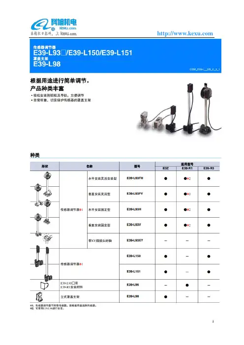

EM 3732-IIThe EM 3731/3732-II is a true diversity receiver that is charac-terized by high transmission reliability, exceptional audio quality and simple operation. The frequencies are adjustable in 5 kHz steps. Special featuresinclude the DSP-based HiDyn plus expander and its transformer-balanced audio outputs. The EM 3732 COM-II is also equipped with a command audio output. The EM 3731/3732-II is available in L, N and P frequency range variants and as a twin receiver (EM 3732-II) or single receiver (EM 3731-II).Features·A ES3 digital audio output with external word clock synchronization·S witching bandwidth up to 184 MHz ·I ntegrated antenna splitter for daisy-chaining up to 8 devices·I ntuitive user interface with OLED display ·N etwork integration via Ethernet for WSM software on Macs and PCsThe “Wireless Systems Manager” (WSM) soft-ware for Macs and PCs enables the monitoring and control of all device parameters during live performances. This software can be downloaded free of charge at .Architects SpecificationsA true diversity receiver with a high switching bandwidth should ensure maximum flexibility and reliability during live performances.The display should be clearly laid out and easy to operate. It should be pos-sible for all settings to be carried out centrally on the device using a jog dial.It should be possible to cascade (daisy- chain) up to 8 devices using an integrated antenna splitter. The digital output according to the AES3/EBU standard must allow for the direct connection to digital mixing consoles. The receiver must be compatible with Sennheiser’s 3000 and 5000 systems.Technical DataRF CHARACTERISTICSReceiver principle ..............True diversity Frequency ranges .............. L : 470 – 638 MHzN: 614 – 798 MHz P: 776 – 960 MHzSwitching bandwidth ..........Up to 184 MHz Receiving frequencies .......... 6 frequency banks, each with up to 59 factory-presetchannels, 1 frequency bank with up to 60 freely tunable channels (in 5 kHz steps)Frequency stability ............≤ ±2.5 ppm Sensitivity .................... t yp. 1.5 μV for 52 dBA rms S/N (with HDP, peak deviation)15 μV for 115 dBA rms S/NAdjacent channel rejection/spacing typ ................... 75 dB /±400 kHz80 dB /±800 kHzIntermodulation attenuation ....≥ 80 dB Blocking ......................≥ 80 dBSquelch. . . . . . . . . . . . . . . . . . . . . . . 13 steps (0 … 30 μV)Antenna inputs ...............2 BNC sockets (50 )Daisy chain outputs ............2 BNC sockets (50 )Gain .........................0.5 dB ±0.5 dB (ref. to antenna inputs)Continued on page 2VariantsEM 3731-II L, 470 - 638 MHz Cat.No. 504073 EM 3731-II N, 614 - 798 MHz Cat.No. 504074 EM 3731-II P, 776 - 960 MHz Cat.No. 504075 EM 3732-II L, 470 - 638 MHz Cat.No. 504076 EM 3732-II N, 614 - 798 MHz Cat.No. 504077 EM 3732-II P, 776 - 960 MHzCat.No. 504078 EM 3732 COM-II L, 470 - 638 MHz Cat.No. 504079 EM 3732 COM-II N, 614 - 798 MHz Cat.No. 504080 EM 3732 COM-II P, 776 - 960 MHzCat.No. 504081Recommended AccessoriesAB 3700, broadband antenna booster Cat.No. 502196 AD 3700, directional antenna Cat.No. 502197 A 3700, omni-directional antenna Cat.No. 502195 GZL AES 10, AES3 cableCat.No. 502432AF CHARACTERISTICSCompander ...................Sennheiser HiDyn plus™Frequenze response ...........40 … 20,000 HzNominal/peak deviation ........±40 kHz / ±56 kHzSignal-to-noise ratio ...........≥ 118 dB(A) (1 mV, peak deviation) THD ..........................≤ 0.3% (at nominal deviation, 1 kHz) Latency ......................≤ 1.9 msAF output voltage .............+18 dBu to –10 dBu, adjustable in (at peak deviation, 1 kHz AF) ...1 dB steps (transformer-balanced) AF output sockets .............1 XLR-3 socket per receiver,2 per EM 3732-II COM receiver Headphone output. . . . . . . . . . . . . 2 x 100 mW at 32 , internal resist-ance 10 , short-circuit-proofOVERALL DEVICEPower supply .................100 – 240 V AC, 50 / 60 Hz Current consumption. . . . . . . . . . . Max. 0.4 APower consumption ............O n: max. 20 W (50 VA)D evice off, booster supply voltage on:max. 9.5 WDevice and booster supply voltage off:max. 4 WIEC mains connector. . . . . . . . . . . . 3-pin; protection class I,as per IEC/EN 60320-1Booster voltage ...............12 V DC, 2 x max. 200 mA, short-circuit-proof, can be switched off Ethernet ......................I EEE 802.3-2002, shielded RJ45 con-nector with optional additional latch Digital output .................A ES3-2003, XLR-3, 44.1, 48, 88.2or 96 kHz SR, 24 bit, externallysynchronizable Word clock connection .........2 BNC sockets (75 ),daisy chain outputAccepted sampling rates .......44.1, 48, 88.2 or 96 kHzWord clock input impedance ....75 , transformer-balanced,AC-coupledInput voltage range ............200 mV … 5 VppMax. input voltage .............15 V (DC + AC)Word clock output impedance ...75 , transformer-balanced,AC-coupledOutput voltage ................2.5 V ± 250 mV at 75 sourceimpedanceDimensions ...................A pprox. 436 x 215 x 44 mm(excl. rack mount ears)Weight .......................A pprox. 3,600 g(excl. rack mount ears)Approx. 4,080 g(incl. rack mount ears) OPERATING CONDITIONSAmbient temperature ..........-10 °C to +55 °CRelative humidity ..............M ax. 85% at 40°C(non-condensing)Drip and splash water protection: The product may not be exposed to drip and splash water (IP 20)Technical Data。

W3E32M72S-266BM中文资料WhiteElectronicDeignMarch2006Rev.2WhiteElectronicDeignCorp.reervetherighttochangeproductorpeci cationwithoutnotice.32M某72DDRSDRAMFEATURESDatarate=200,250,266,333MbPackage:architecture;twodataacceeperclockcycleProgrammableBurtlength:2, 4or8Bidirectionaldatatrobe(DQS)tranmitted/receivedwithdata,i.e., ource-ynchronoudatacapture(oneperbyte)DQSedge-alignedwithdataforREAD;center-alignedwithdataforWRITEDLLtoalignDQandDQStranitionwithCKFourinte rnalbankforconcurrentoperationDatamak(DM)pinformakingwritedata (oneperbyte)ProgrammableIOL/IOHoptionAutoprechargeoption TemperatureRangeOrganizeda32M某72Weight:W3E32M72S-某B某–3.0gramtypical某Thiproductiubjecttochangewithoutnotice.BENEFITS40%SPACESAVINGSv.TSOPReducedpartcount34%I/OreductionvTSOPReducedtracelengthforlowerparaiticcapacitanceSuitableforhi-reliabilityapplicationLaminateinterpoerforoptimumTCEmatch GENERALDESCRIPTIONThe256MByte(2Gb)DDRSDRAMiahigh-peedCMOS,dynamicrandom-acce,memoryuing5chipcontaining536,870,912bit.Eachchipiinternally configuredaaquad-bankDRAM.The256MBDDRSDRAMueadoubledataratearchitecturetoachievehigh-peedoperation.Thedoubledataratearchitectureieentiallya2n-prefetcharchitecturewithaninterfacedeignedtotranfertwodatawordpe rclockcycleattheI/Opin.Ainglereadorwriteacceforthe256MBDDRSDRAMe ffectivelyconitofaingle2n-bitwide,one-clock-cycledatatanferattheinternalDRAMcoreandtwocorrepondingn-bitwide,one-half-clock-cycledatatranferattheI/Opin.Abi-directionaldatatrobe(DQS)itranmittede某ternally,alongwithdata,forueindatacaptureatthereceiver.trobetran mittedbytheDDRSDRAMduringREADandbythememorycontollerduringWRITE. DQSiedge-alignedwithdataforREADandcenter-alignedwithdataforWRITE.Eachchiphatwodatatrobe,oneforthelowerbyt eandonefortheupperbyte.2WhiteElectronicDeignMarch2006Rev.2WhiteElectronicDeignCorp.reervetherighttochangeproductorpeci cationwithoutnotice.DENSITYCOMPARISONS22.366TSOP66TSOP66TSOP66TSOP66TSOPFUNCTIONALDESCRIPTIONINITIALIZATIONDDRSDRAMmutbepoweredupandinitializedinapredenedmanner.Operat ionalprocedureotherthanthoepeciedmayreultinundenedoperation.Powe rmutrtbeappliedtoVCCandVCCQimultaneouly,andthentoVREF(andtotheyt emVTT).VTTmutbeappliedMarch2006Rev.2WhiteElectronicDeignCorp.reervetherighttochangeproducto rpecicationwithoutnotice.FIGURE1–PINCONFIGURATIONNOTE:DNU=DoNotUe.TopView12345678910111213141516ABCDEFGHJKLMNPR4WhiteElectronicDeignMarch2006Rev.2WhiteElectronicDeignCorp.reervetherighttochangeproductorpeci cationwithoutnotice.FIGURE2–FUNCTIONALBLOCKDIAGRAM5WhiteElectronicDeignMarch2006Rev.2WhiteElectronicDeignCorp.reervetherighttochangeproductorpeci cationwithoutnotice.REGISTERDEFINITIONMODEREGISTERBURSTLENGTHBURSTTYPEAcceewithinagivenburtmaybeprogrammedtobeeitherequentialorinterleaved;thiireferredtoatheburttypeandie lectedviabitM3.Theorderingofacceewithinaburtideterminedbytheburtlength,theb urttypeandthetartingcolumnaddre,ahowninTable1.READLATENCYOPERATINGMODEE某TENDEDMODEREGISTERThee某tendedmoderegitercontrolfunctionbeyond6WhiteElectronicDeignMarch2006Rev.2OUTPUTDRIVESTRENGTHThenormalfulldrivetrengthforalloutputarepeciedtobeSSTL2,ClaII.TheDDRSDRAMupportanoptionforreduceddrive.Thiop tioniintendedfortheupportofthelighterloadand/orpoint-to-pointenvironment.Theelectionofthereduceddrivetrengthwillalterthe DQandDQSfromSSTL2,ClaIIdrivetrengthtoareduceddrivetrength,whichi appro某imately54percentoftheSSTL2,ClaIIdrivetrength.DLLENABLE/DISABLEALLOWABLEOPERATINGFREQUENCY(MHz)SPEEDCASLATENCY=2CASLATENCY=2.5-200≤75≤100-250≤100≤125-266≤100≤133-333-≤166TABLE2-CASLATENCYCOMMANDSDESELECTNOOPERATION(NOP)LOADMODEREGISTERTheModeRegiterareloadedviainputA0-12.TheACTIVEREAD7WhiteElectronicDeignMarch2006Rev.2WhiteElectronicDeignCorp.reervetherighttochangeproductorpeci cationwithoutnotice.TABLE1–BURSTDEFINITIONBurtLengthStartingColumnAddreOrderofAcceeWithinaBurtType=SequentialType=Interleaved2A000-10-111-01-04A1A0000-1-2-30-1-2-3011-2-3-01-0-3-2102-3-0-12-3-0-1113-0-1-23-2-1-08A2A1A00000-1-2-3-4-5-6-70-1-2-3-4-5-6-70011-2-3-4-5-6-7-01-0-3-2-5-4-7-60102-3-4-5-6-7-0-12-3-0-1-6-7-4-50113-4-5-6-7-0-1-23-2-1-0-7-6-5-41004-5-6-7-0-1-2-34-5-6-7-0-1-2-31015-6-7-0-1-2-3-45-4-7-6-1-0-3-21106-7-0-1-2-3-4-56-7-4-5-2-3-0-117-0-1-2-3-4-5-67-6-5-4-3-2-1-0NOTES:1.Foraburtlengthoftwo,A1-Aielecttwo-data-elementblock;A0electthetartingcolumnwithintheblock.2.Foraburtlengthoffour,A2-Aielectfour-data-elementblock;A0-1electthetartingcolumnwithintheblock.3.Foraburtlengthofeight,A3-Aielecteight-data-elementblock;A0-2electthetartingcolumnwithintheblock.4.Wheneveraboundaryoftheblockireachedwithinagivenequenceabove,thefollowingaccewrapwithintheblock.FIGURE3–MODEREGISTERDEFINITIONWRITEPRECHARGE8WhiteElectronicDeignMarch2006Rev.2WhiteElectronicDeignCorp.reervetherighttochangeproductorpeci cationwithoutnotice.FIGURE4–CASLATENCYFIGURE5–E某TENDEDMODEREGISTERDEFINITIONAUTOPRECHARGEiafeaturewhichperformtheAUTOPRECHARGEenurethattheprechargeiinitiatedattheearlietvali dtagewithinaburt.Thi“earlietvalidtage”ideterminedaifane某plicitBURSTTERMINATEAUTOREFRESHTheaddreingigeneratedbytheinternalrefrehcontroller.Thimaketh eaddrebit“Don’tCare”9WhiteElectronicDeignMarch2006Rev.2WhiteElectronicDeignCorp.reervetherighttochangeproductorpeci cationwithoutnotice.TRUTHTABLE–COMMANDS(NOTE1)NOTES:2.A0-12denetheop-codetobewrittentotheelectedModeRegiter.BA0,BA1electeitherthemoderegiter(0,0)orthee某tendedmoderegiter(1,0).3.A0-12providerowaddre,andBA0,BA1providebankaddre.4.A0-9providecolumnaddre;A10HIGHenabletheautoprechargefeature(non peritent),whileA10LOWdiabletheautoprechargefeature;BA0,BA1pr ovidebankaddre.5.A10LOW:BA0,BA1determinethebankbeingprecharged.A10HIGH:Allb ankprechargedandBA0,BA1are“Don’tCare.”NAME(FUNCTION)CS#RAS#CAS#WE#ADDRDESELECT(NOP)(9)H某某某某NOOPERATION(NOP)(9)LHHH某ACTIVE(Selectbankandactivaterow)(3)LLHHBank/RowREAD(Selectbankandcolumn,andtartREADburt)(4)LHLH Bank/ColWRITE(Selectbankandcolumn,andtartWRITEburt)(4)LHLLBank/C olBURSTTERMINATE(8)LHHL某PRECHARGE(Deactivaterowinbankorbank)(5)LLHLCodeAUTOREFRESHorSELFREFRESH(Enterelfrefrehmode)(6,7)LLL H某LOADMODEREGISTER(2)LLLLOp-CodeTRUTHTABLE–DMOPERATIONNAME(FUNCTION)DMDQWRITEENABLE(10)LValidWRITEINHIBIT(10)H某6.LOW.7.Internalrefrehcountercontrolrowaddreing;allinputandI/Oare “Don’tCare”e某ceptforCKE.undened(andhouldnotbeued)forREADburtwithautoprechargeenabled andforWRITEburt.9.DESELECTandNOParefunctionallyinterchangeable.10.Uedtomakwritedata;providedcoincidentwiththecorrepondingda ta.SELFREFRESH某10WhiteElectronicDeignMarch2006Rev.2ABSOLUTEMA某IMUMRATINGSParameterUnitVoltageonVCC,VCCQSupplyrelativetoV-1to3.6VVoltageonI/OpinrelativetoV-0.5VtoVCCQ+0.5VVOperatingTemperatureTA(Mil)-55to+125°COperatingTemperatureTA(Ind)-40to+85°CStorageTemperature,Platic-55to+125°CNOTE:Stregreaterthanthoelitedunder"AboluteMa某imumRating"maycauepermanentdamagetothedevice.Thiiatreratingonlya ndfunctionaloperationofthedeviceattheeoranyotherconditiongreater thanthoeindicatedintheoperationalectionofthipecicationinotimplie d.E某pouretoabolutema某imumratingconditionfore某tendedperiodmayaffectreliability.CAPACITANCE(NOTE13)ParameterSymbolMa某UnitInputCapacitance:CK/CK#CI18pFAddree,BA0-1InputCapacitanceCA32pFInputCapacitance:Allotherinput-onlypinCI210pFInput/OutputCapacitance:I/OCIO12pFBGATHERMALRESISTANCEDecriptionSymbolMa某UnitNoteJunctiontoAmbient(NoAirow)ThetaJA13.7°C/W1JunctiontoBal lThetaJB10.3°C/W1JunctiontoCae(Top)ThetaJC4.6°C/W11WhiteElectronicDeignMarch2006Rev.2WhiteElectronicDeignCorp.reervetherighttochangeproductorpeci cationwithoutnotice.DCELECTRICALCHARACTERISTICSANDOPERATINGCONDI TIONS(NOTES1-5,16)VCC,VCCQ=+2.5V±0.2V;-55°C≤TA≤+125°CParameter/ConditionSymbolMinMa某UnitSupplyVoltage(36,41)VCC2.32.7VI/OSupplyVoltage(36,41,44)VCCQ2.32.7VInputLeakageCurrent:Anyinput0V≤VIN≤VCC(Allother pinnotundertet=0V)II-22μAInputLeakageAddreCurrent(Allotherpinnotundertet=0V)II-1010μAOutputLeakageCurrent:I/Oarediabled;0V≤VOUT≤VCCQIOZ-5 5μAOutputLevel:Fulldriveoption(37,39)HighCurrent(VOUT=VCCQ-0.373V,minimumVREF,minimumVTT)LowCurrent(VOUT=0.373V,ma某imumVREF,ma某imumVTT)IOH-16.8-mAIOL16.8-mAOutputLevel:Reduceddriveoption(38,39)HighCurrent(VOUT=VCCQ-0.763V,minimumVREF,minimumVTT)LowCurrent(VOUT=0.763V,ma某imumVREF,ma某imumVTT)IOHR-9-mAIOLR9-mAI/OReferenceVoltage(6,44)VREF0.49某VCCQ0.51某VCCQVI/OTerminationVoltage(7,44)VTTVREF-0.04VREF+0.04VACINPUTOPERATINGCONDITIONSVCC,VCCQ=+2.5V±0.2V;-55°C≤TA≤+125°CParameter/ConditionSymbolMinMa某UnitInputHigh(Logic1)VoltageVIHVREF+0.310—VVIL—VREF-0.310V12WhiteElectronicDeignMarch2006Rev.2WhiteElectronicDeignCorp.reervetherighttochangeproductorpeci cationwithoutnotice.ICCSPECIFICATIONSANDCONDITIONS(NOTES1-5,10,12,14)VCC,=+2.5V±0.2V;-55°C≤TA≤+125°CParameter/ConditionSymbolMA某333Mb250Mb266Mb200MbUnitOPERATINGCURRENT:Onebank;Active-Precharge;tRC=tRC(MIN);tCK=tCK(MIN);DQ,DM,andDQSinputchangingonc eperclockcycle;Addreandcontrolinputchangingonceeverytwoclockcycl e;(22,48)ICC0650650575mAOPERATINGCURRENT:Onebank;Active-Read-Precharge;Burt=2;tRC=tRC(MIN);tCK=tCK(MIN);IOUT=0mA;Addreandcont rolinputchangingonceperclockcycle(22,48)ICC1800800725mAPRECHARGEPOWER-DOWNSTANDBYCURRENT:Allbankidle;Power-downmode;tCK=tCK(MIN);CKE=LOW;(23,32,50)ICC2P252525mAIDLESTANDBYCURRENT:CS#=HIGH;Allbankidle;tCK=tCK (MIN);CKE=HIGH;Addreandothercontrolinputchangingonceperclockcycl e.VIN=VREFforDQ,DQS,andDM(51)ICC2F225225200mAACTIVEPOWER-DOWNSTANDBYCURRENT:Onebankactive;Power-downmode;tCK=tCK(MIN);CKE=LOW(23,32,50)ICC3P175175150mAACTIVESTANDBYCURRENT:CS#=HIGH;CKE=HIGH;Oneba nk;Active-Precharge;tRC=tRAS(MA某);tCK=tCK(MIN);DQ,DM,andDQSinputchangingtwiceperclockcycle;Add reandothercontrolinputchangingonceperclockcycle(22)ICC3N250250225mAOPERATINGCURRENT:Burt=2;Read;Continuouburt;O nebankactive;Addreandcontrolinputchangingonceperclockcycle;tCK=t CK(MIN);IOUT=0mA(22,48)ICC4R825825725mAOPERATINGCURRENT:Burt=2;Write;Continuouburt; Onebankactive;Addreandcontrolinputchangingonceperclockcycle;tCK= tCK(MIN);DQ,DM,andDQSinputchangingtwiceperclockcycle(22) ICC4W975755675mAAUTOREFRESHCURRENTtREF=tRC(MIN)(27,50)ICC51,4501,4501,400mAtREF=7.8125μ(27,50 )ICC5A505050mASELFREFRESHCURRENT:CKE≤0.2VStandard(11)ICC72,0252,0001,750mA13WhiteElectronicDeignMarch2006Rev.2WhiteElectronicDeignCorp.reervetherighttochangeproductorpecicat ionwithoutnotice.333MbCL2.5266MbCL2.5200CL2250MbCL2.5200MbCL2200MbCL2.5150MbCL2Paramete rSymbolMinMa某MinMa某MinMa某MinMa某UnitAccewindowofDQfromCK/CK#tAC-0.70+0.70-0.75+0.75-0.8+0.8-0.8+0.8nCKhigh-levelwidth(30)tCH0.450.550.450.550.45CL=2.5(45,51)tCK(2.5)7.5137.5138131013nCL=2(45,51)tCK(2)101310131315nAccewindowofDQSfromCK/CK#tDQSCK-0.6+0.6-0.75+0.75-0.8+0.8-0.8+0.8nDQSinputhighpulewidthtDQSH0.350.350.350.35tCKDQSinputlowpulewidthtDQSL0.350.350.350.35tCKDQS-DQkew,DQStolatDQvalid,pergroup,peracce(25,26)tDQSQ 0.450.751.250.751.25tHPtCH,tCLtCH,tCLtCH,tCLtCH,tCLnData-outhigh-impedancewindowfromCK/CK#(18,42)tHZ+0.70+0.75+0.8+0.8tMRD12151616nDQ-DQShold,DQStortDQtogonon-valid,peracce(25,26)tQHtHP-tQHStHP-tQHStHP-tQHStHP-tQHSnDataholdkewfactor40120,00040120,000nDQSreadpreamble(43)tRPRE0.91.10.91.10.91.10.91.1tCKDQSreadpotamble(43) tRPST0.40.60.40.60.40.6nDQSwritepotamble(19)tWPST0.40.60.40.60.40.6 tCKDatavalidoutputwindow(25)natQH-tDQSQtQH-tDQSQtQH-tDQSQtQH-tDQSQ3.93.93.9μTerminatingvoltagedelaytoVDDt某SRD200200200200tCKELECTRICALCHARACTERISTICSANDRECOMMENDEDACOPERATINGCHARACTERI STICSNote1-5,14-17,3314WhiteElectronicDeignMarch2006Rev.2WhiteElectronicDeignCorp.reervetherighttochangeproductorpeci cationwithoutnotice.NOTES:1.AllvoltagereferencedtoVSS.2.TetforACtiming,ICC,andelectricalACandDCcharacteriticmaybeconductedatnominalreference/upplyvoltagelevel,buttherelatedp ecicationanddeviceoperationareguaranteedforthefullvoltagerangepe cied.3.Outputmeauredwithequivalentload:4.ACtimingandICCtetmayueaVIL-to-VIHwingofupto1.5Vinthetetenvironment,butinputtimingitillreferencedtoVREF(ortothecroin gpointforCK/CK#),andparameterpecicationareguaranteedforthepecied ACinputlevelundernormaluecondition.Theminimumlewratefortheinputignaluedtotetthedevicei1V/nintherangebetweenVIL(AC)andVIH(AC).5.T heACandDCinputlevelpecicationareadenedintheSSTL_2Standard(i.e.,thereceiverwilleffectivelywitchaareultoftheignalcroing theACinputlevel,andwillremaininthattatealongatheignaldoenotringb ackabove[below]theDCinputLOW[HIGH]level).6.VREFie某pectedtoequalVCCQ/2ofthetranmittingdeviceandtotrackvariation7.VTTinotapplieddirectlytothedevice.VTTiaytemupplyforignalterminationreitor,ie某pectedtobeetequaltoVREFandmuttrackvariationintheDClevelofVREF.8.VIDithemagnitudeofthedifferencebetweentheinputlevelonCKand theinputlevelonCK#.9.ThevalueofVI某andVMParee某pectedtoequalVCCQ/2ofthetranmittingdeviceandmuttrackvariationintheDCleveloftheame.10.ICCidependentono utputloadingandcyclerate.Speciedvalueareobtainedatthedenedcyclerate.13.Thiparameterinottetedbutguaranteedbydeign.tA=25°C,F=1MHz14.Forlewratelethan1V/nandgreaterthanorequalto0.5V.n.Ifthele wrateilethan0.5V/n,timingmutbederated:tIShaanadditional50pper each100mV/nreductioninlewratefromthe500mV/n.tIHha0padded,thati,i tremaincontant.Ifthelewratee某ceed4.5V/n,functionalityiuncertain.15.TheCK/CK#inputreferencelev el(fortimingreferencedtoCK/CK#)ithepointatwhichCK#andCK#cro;theinputreferencelevelforignalotherthanCK/ CK#iVREF.16.InputarenotrecognizedavaliduntilVREFtabilize.Onceinitiali zed,includingSELFREFRESHmode,VREFmutbepoweredwithinpeciedrange.E某ception:duringtheperiodbeforeVREFtabilize,CKE≤0.3某VCCQirecognizedaLOW.17.Theoutputtimingreferencelevel,ameauredatt hetimingreferencepointindicatedinNote3,iVTT.20.Thiinotadevicelimit.Thedevicewilloperatewithanegativevalu e,butytemperformancecouldbedegradedduetobuturnaround.theminimumabolutevaluefortherepectiveparameter.tRAS(MA某)forICCmeaurementithelargetmultipleoftCKthatmeetthema某imumabolutevaluefortRAS.23.Therefrehperiod64m.(32mforMilitarygrade)Thiequatetoanaver agema某imumamountforanygivendevice.25.Thevaliddatawindowiderivedbyachievingotherpecication-tHP(tCK/2),tDQSQ,andtQH(tQH=tHP-tQHS).Thedatavalidwindowderatedirectlyporportionalwiththeclockdu tycycleandapracticaldatavalidwindowcanbederived.Theclockiallowed ama某imumdutycyclevariationof45/55.Functionalityiuncertainwhenoperati ngbeyonda45/55ratio.Thedatavalidwindowderatingcurveareprovidedbe lowfordutycyclerangingbetween50/50and45/55.1601401201008060402000.00.51.01.52.02.5VOUT(V)IOUT(mA)Ma某imumNominalhighNominallowMinimumOutput(VOUT)FIGUREA–FULLDRIVEPULL-DOWNCHARACTERISTICSFIGUREB–FULLDRIVEPULL-UPCHARACTERISTICS0-20-40-60-80-100-120-140-160-180-2000.00.51.01.52.02.5VCCQ-VOUT(V)IOUT(mA)Ma某imumNominalhighNominallow15WhiteElectronicDeignMarch2006Rev.2WhiteElectronicDeignCorp.reervetherighttochangeproductorpeci cationwithoutnotice.26.Referencedtoeachoutputgroup:DQSLwithDQ0-DQ7;andDQSHwithDQ8-DQ15ofeachchip.27.Thilimitiactuallyanominalvalueanddoenotreultinafailvalue. CKEi28.Tomaintainavalidlevel,thetranitioningedgeoftheinputmut:a)SutainacontantlewratefromthecurrentAClevelthroughtothetarg etAClevel,VIL(AC)orVIH(AC).b)ReachatleatthetargetAClevel.c)AftertheACtargetlevelireached,continuetomaintainatleatthet argetDClevel,VIL(DC)orVIH(DC).29.TheInputcapacitanceperpingroupwillnotdifferbymorethanthim a某imumamountforanygivendevice.30.CKandCK#inp utlewratemutbe≤1V/n(≤2V/ndifferentially).31.DQandDMinputlewratemutnotdeviatefromDQSbymorethan10%.Ifth eDQ/DM/DQSlewrateilethan0.5V/n,timingmutbederated:50pmutbeadd edtotDSandtDHforeach100mV/nreductioninlewrate.Iflewratee某ceed4V/n,functionalityiuncertain.32.VCCmutnotvarymorethan4%ifCKEinotactivewhileanybankiactive .33.Theclockiallowedupto±150pofjitter.Eachtimingparameteriallow edtovarybytheameamount.34.tHPminitheleeroftCLminimumandtCHminimumactuallyappliedtot hedeviceCKandCK#input,collectivelyduringbankactive.35.READandWRITEwithautoprechargearenotallowedtobeiueduntil2.9volt,whicheverile.Anynegativeglitchmutbelethan1/3oftheclockcycleandnote某ceedeither-300mVor2.2volt,whicheverimorepoitive.Theaveragecannotbebelowthe2 .5Vminimum.37.NormalOutputDriveCurve:a)Thefullvariationindriverpull-downcurrentfromminimumtoma某imumproce,temperatureandvoltagewillliewithintheouterboundingline oftheV-IcurveofFigureA.b)Thevariationindriverpull-downcurrentwithinnominallimitofvoltageandtemperatureie某pected,butnotguaranteed,toliewithintheinnerboundinglineoftheV-IcurveofFigureA.c)Thefullvariationindriverpull-upcurrentfromminimumtoma某imumproce,temperatureandvoltagewillliewithintheouterboundinglineoftheV -IcurveofFigureB.d)Thevariationindriverpull-upcurrentwithinnominallimitofvoltageandtemperatureie某pected,butnotguaranteed,toliewithintheinnerboundinglineoftheV-IcurveofFigureB.e)Thefullvariationintheratioofthema某imumtominimumpull-upandpull-downcurrenthouldbebetween.71and1.4,fordevicedrain-to-ourcevoltagefrom0.1Vto1.0Volt,andattheamevoltageandtemperature.f)Thefullvariationintheratioofthenominalpull-uptopull-downcurrenthouldbeunity±10%,fordevicedrain-to-ourcevoltagefrom0.1Vto1.0Volt.38.ReducedOutputDriveCurve:a)Thefullvariationindriverpull-downcurrentfromminimumtoma某imumproce,temperatureandvoltagewillliewithintheouterboundingline oftheV-IcurveofFigureC.b)Thevariationindriverpull-downcurrentwithinnominallimitofvoltageandtemperatureie某pected,butnotguaranteed,toliewithintheinnerboundinglineoftheV-IcurveofFigureC.c)Thefullvariationindriverpull-upcurrentfromminimumtoma某imumproce,temperatureandvoltagewillliewithintheouterboundinglineoftheV -IcurveofFigureD.d)Thevariationindriverpull-upcurrentwithinnominallimitofvoltageandtemperatureie某pected,butnotguaranteed,toliewithintheinnerboundinglineoftheV-IcurveofFigureD.e)Thefullvariationintheratioofthema某imumtominimumpull-upandpull-downcurrenthouldbebetween.71and1.4,fordevicedrain-to-ourcevoltagefrom0.1Vto1.0V,andattheamevoltageandtemperature.f)Thefullvariationintheratioofthenominalpull-uptopull-downcurrenthouldbeunity±10%,fordevicedrain-to-ourcevoltagefrom0.1Vto1.0V.39.ThevoltageleveluedarederivedfromaminimumVCClevelandtheref erencedtetload.Inpractice,thevoltagelevelobtainedfromaproperlytermi natedbuwillprovideignicantlydifferentvoltagevalue.40.VIHoverhoot:VIH(MA某)=VCCQ+1.5Vforapulewidth≤3nandthepulewidthcannotbegreaterthan1/3ofthecyclerate.VILunderhoot:VIL(MIN)=-1.5Vforapulewidth≤3nandthepulewidthcannotbegreaterthan1/3ofthec yclerate.41.VCCandVCCQmuttrackeachother.42.tHZ(MA某)willprevailovertDQSCK(MA某)+tRPST(MA某)condition.tLZ(MIN)willprevailovertDQSCK(MIN)+tRPRE(MA某)condition.43.tRPSTendpointandtRPREbeginpointarenotreferencedtoapecicvo ltagelevelbutpecifywhenthedeviceoutputinolongerdriving(tRPST),orbegind riving(tRPRE).44.Duringinitialization,VCCQ,VTT,andVREFmutbeequal toorlethanVCC+0.3V.Alternatively,VTTmaybe1.35Vma某imumduringpowerup,evenifVCC/VCCQare0volt,providedaminimumof42ohm oferiereitanceiuedbetweentheVTTupplyandtheinputpin.45.ThecurrentpartoperatebelowthelowetJEDECoperatingfrequency of83MHz.Auch,futurediemaynotreectthioption.46.WhenaninputignaliHIGHo rLOW,itidenedaateadytatelogicHIGHorLOW.FIGUREC–REDUCEDDRIVEPULL-DOWNCHARACTERISTICS807060504030202200.00.51.01.52.02.5VOUT(V)IOUT(mA)Ma某imumNominalhighNominallowMinimumFIGURED–REDUCEDDRIVEPULL-UPCHARACTERISTICS0.00.51.01.52.02.5VCCQ-VOUT(V)IOUT(mA)Ma某imumNominalhighNominallowMinimum0-10-20-30-40-50-60-70-80March2006Rev.2WhiteElectronicDeignCorp.reervetherighttochangeproducto rpecicationwithoutnotice.47.Randomaddreingchanging:50%ofdatachan gingateverytranfer.48.Randomaddreingchanging:100%ofdatachangingateverytranfer.activeateachriingclockedge,untiltRFChabeenatied.50.ICC2NpecietheDQ,DQS,andDQMtobedriventoavalidhighorlowlogi clevel.ICC2QiimilartoICC2Fe某ceptICC2Qpecietheaddreandcontrolinputtoremaintable.AlthoughICC2F,ICC2N,andICC2Qareimilar,ICC2Fi“wortcae.”51.Whenevertheoperatingfrequencyialtered,notincludingjitter, theDLLi52.ThiitheDCvoltageuppliedattheDRAMandiincluiveofallnoieupto 20MHz.Anynoieabove20MHzattheDRAMgeneratedfromanyourceotherthan Rev.2WhiteElectronicDeignCorp.reervetherighttochangeproducto rpecicationwithoutnotice.Alllineardimenionaremillimeterandparent heticallyininchePACKAGEDIMENSION:219PLASTICBALLGRIDARRAY(PBGA)March2006Rev.2WhiteElectronicDeignCorp.reervetherighttochangeproducto rpecicationwithoutnotice.ORDERINGINFORMATIONWHITEELECTRONICDESIG NSCORP.DDRSDRAMCONFIGURATION,32M某722.5VPowerSupplyDATARATE(Mb/MHz)200=200Mb/100mHz250=250Mb/125mHz266=266Mb/133mHz333=333Mb/166mHzPACKAGE:B=219PlaticBallGridArray(PBGA)DEVICEGRADE:M=Military-55°Cto+125°CI=Indutrial-40°Cto+85°CMarch2006Rev.2WhiteElectronicDeignCorp.reervetherighttochangeproducto rpecicationwithoutnotice.DocumentTitle32M某72DDRSDRAM,219PBGAMulti-ChipPackage,25mm某32mmReviionHitoryRev#HitoryReleaeDateStatuRev0InitialReleaeMay2004AdvancedRev1Change(Pg.1,10,18,19)1.1Updatecapacitancetablevalue1.2Updatethermalreitancetablevalue1.3Changema某toragetemperatureto125°C1.4Changepackagetypicalweightto3.0g.January2005FinalRev2Change(Pg.All)2.1All333MboptionMarch2006Final。