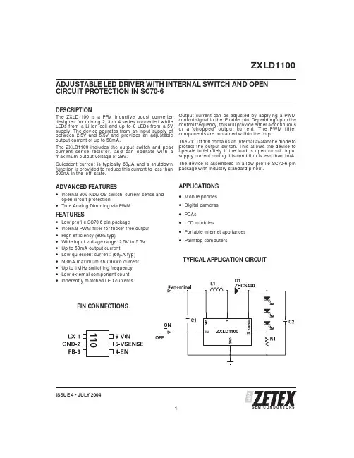
1S E M I C O N D U C T O R SDESCRIPTIONThe ZXLD1100is a PFM inductive boost converter designed for driving 2,3or 4series connected white LEDs from a Li-Ion cell and up to 8LEDs from a 5V supply.The device operates from an input supply of between 2.5V and 5.5V and provides an adjustable output current of up to 50mA.The ZXLD1100includes the output switch and peak current sense resistor,and can operate with a maximum output voltage of 28V.Quiescent current is typically 60A and a shutdown function is provided to reduce this current to less than 500nA in the 'off' state.ADVANCED FEATURES•Internal 30V NDMOS switch, current sense andopen circuit protection•True Analog Dimming via PWMFEATURES•Low profile SC70 6 pin package•Internal PWM filter for flicker free output •High efficiency (80% typ)•Wide input voltage range: 2.5V to 5.5V •Up to 50mA output current•Low quiescent current: (60A typ)•500nA maximum shutdown current •Up to 1MHz switching frequency •Low external component count •Inherently matched LED currentsOutput current can be adjusted by applying a PWM control signal to the 'Enable'pin.Depending upon the control frequency,this will provide either a continuous or a 'chopped'output current.The PWM filter components are contained within the chip.The ZXLD1100contains an internal avalanche diode to protect the output switch.This allows the device to operate indefinitely if the load is open circuit.Input supply current during this condition is less than 1mA.The device is assembled in a low profile SC70-6pin package with industry standard pinout.APPLICATIONS•Mobile phones •Digital cameras •PDAs •LCD modules•Portable internet appliances •Palmtop computersZXLD1100ISSUE 4 - JULY 2004ADJUSTABLE LED DRIVER WITH INTERNAL SWITCH AND OPENCIRCUIT PROTECTION IN SC70-6PIN CONNECTIONSTYPICAL APPLICATION CIRCUITZXLD1100S E M I C O N D U C T O R SISSUE 4 - JULY 20042PARAMETER SYMBOL LIMIT UNIT Input voltage (V IN )7V LX output voltage (V LX )30V Switch output current (I LX )500mA Power dissipation (PD)300mW Operating temperature (T OP )-40 to 85°C Storage temperature (T ST )-55 to 150°C Junction temperature(T j MAX )125°CABSOLUTE MAXIMUM RATINGS (Voltages to GND unless otherwise stated)DEVICE DEVICE DESCRIPTION TEMPERATURE RANGEPART MARKTAPING OPTIONS ZXLD1100H6Boost convertor in SC70-6-40 to +85°C110TA, TCORDERING INFORMATIONZXLD1100H6TA = 7” reel of 3,000 devices ZXLD1100H6TC = 13” reel of 10,000 devicesZXLD1100S E M I C O N D U C T O R SISSUE 4 - JULY 20043SYMBOL PARAMETER CONDITIONSMIN.TYP .MAX.UNIT V IN Input voltage 2.55.5VI INSupply currentQuiescent ShutdownV EN =V IN ,I LX =0,Output not switching V EN =0V60100500A nA V FB FB pin control voltage 90.5109.5mV I FB FB pin input current 100nA f LX Operating frequency L=10H,V OUT =10V,I OUT =20mA0.351MHz T OFF LX output 'OFF'time 350500ns T ON LX output 'ON'time (2)5µs I LXpk Switch peak current limit L=10H,V OUT =10V,I OUT =20mA320mA R LX Switch 'On'resistance 1.5⍀I LX(leak)Switch leakage current V LX =20V1µA V OUTController output voltageNormal operation VSENSE pin open-circuit or grounded28VV OUT(MAX)Controller output voltage with outputopen circuit (3)VSENSE connected to Vout2530V V ENH EN pin High level Input voltage Device active 1.5V IN V V ENL EN pin Low level Input voltage Device in shutdown 0.4V I ENL EN pin Low level input current V EN =0V-100nA I ENH EN pin High level input current V EN =V IN1A T EN(hold)EN pin turn off delay(4)V EN switched from high to low120µs ∆T/T PWM duty cycle range at ‘EN’input for filtered PWM control (5)10kHz <f <100kHz,V ENH =V IN20100%f LPF Internal PWM low pass filter cut-off frequency 4kHz A LPFFilter attenuationf=30kHz52.5dBELECTRICAL CHARACTERISTICS (at V IN = 3V , T amb = 25°C unless otherwise stated (1))NOTES:(1) Production testing of the device is performed at 25°C. Functional operation of the device over a -40°C to +85°C temperature range is guaranteed by design, characterization and process control.(2) Nominal 'on' time (T ONnom ) is defined by the input voltage (V IN ), coil inductance (L) and peak current (I LXpkdc ) according to the expression:T ONnom = {I LX(pkdc ) x L/V IN } +200ns.(3) When using the open circuit protection feature, the maximum output voltage under normal operation should be maintained below the minimum value specified, in order to prevent possible disturbance of the current control loop.(4) This is the time for which the device remains active after the EN pin has been asserted low. This delay is necessary to allow the output to be maintained during dc PWM mode operation.(5)The minimum PWM signal frequency during this mode of operation is to ensure that the device remains active during PWM control. This provides a continuous dc output current. For lower frequencies, the device will be gated 'on' and 'off' during PWM control.(6)The maximum PWM signal frequency during this mode of operation should be kept as low as possible to minimize errors due to the turn-off delay of the device (see Enable pin turn-off delay).ZXLD1100S E M I C O N D U C T O R SISSUE 4 - JULY 20044BLOCK DIAGRAMPIN DESCRIPTIONDEVICE DESCRIPTIONThe device is a PFM flyback dc-dc boost converter, working in discontinuous mode.With reference to the chip block diagram and typical application circuit,the operation of the device is as follows:Control loopWhen'EN'is high,the control circuits become active and the low side of the coil(L1)is switched to ground via NDMOS transistor(MN).The current in L1is allowed to build up to an internally defined level (nominally320mA)before MN is turned off.The energy stored in L1is then transferred to the output capacitor (C2)via schottky diode(D1).When the voltage on C2 has risen above the threshold voltage of the series connected LEDs,current will flow through external sense resistor R1.The voltage developed across R1is sensed at pin'FB'and compared to a100mV reference voltage(V REF).A comparator senses when the feedback voltage is above V REF and its output is used to control the'off'time of the output switch.The control loop is self-oscillating,producing pulses of up to5s maximum duration(switch'on'),at a frequency that varies in proportion to the LED current.The feedback loop maintains a voltage of V REF at the FB pin and therefore defines a maximum LED current equal to V REF divided by R1.The minimum'off'time of the output switch is fixed at0.5s nominal,to allow time for the coil's energy to be dissipated before the switch is turned on again.This maintains stable and efficient operation in discontinuous mode.Open circuit protectionThere is an internal avalanche diode between the V SENSE and FB pins of the device.This diode,together with the associated resistors provides open circuit protection when the V SENSE pin is connected to the output voltage.In the event of an open circuit condition,the output voltage will rise above the breakdown voltage of the internal diode,which will then conduct and override the control signal from the current sense resistor.This maintains the output voltage at a level below the breakdown voltage of the output switch.Supply current in this condition will fall to a low value as the control loop provides only the bias current for the diode.Filtered PWM operationThe input of an internal low pass filter is switched to V REF when the EN pin is high and switched to ground when the EN pin is low.The output of this filter drives the comparator within the control loop.A continuous high state on EN therefore provides a filtered voltage of value V REF to the comparator.However,by varying the duty cycle of the EN signal at a suitably high frequency (f>10kHz),the control loop will see a voltage,that has an average value equal to the duty cycle multiplied by V REF.This provides a means of adjusting the output current to a lower value.It also allows the device to be both turned on and adjusted with a single signal at the 'EN'pin.The output during this mode of operation will be a dc current equal to (V REF/R1) x duty cycleGated PWM operationThe internal circuitry of the ZXLD1100is turned off when no signal is present on the'EN'pin for more than 120s(nominal).A low frequency signal applied to the EN pin will therefore gate the device'on'and'off'at the gating frequency and the duty cycle of this signal can be varied to provide a'chopped'output current equal to(V REF/R1)x duty cycle.For best accuracy,the gating frequency should be made as low as possible(e.g. below1kHz),such that the turn off delay of the chip is only a small proportion of the gating periodFurther details of setting output current are given in the applications section under brightness control.ZXLD1100S E M I C O N D U C T O R SISSUE 4 - JULY 20045ZXLD1100S E M I C O N D U C T O R SISSUE 4 - JULY 2004 6TYPICAL CHARACTERISTICS(For typical application circuit at V IN=3V and TA=25 °C unless otherwise stated)ZXLD1100S E M I C O N D U C T O R SISSUE 4 - JULY 20047TYPICAL OPERATING CHARACTERISTICS(For typical applications circuit at V IN =3V, L=10H Coilcraft DO1608C Series, 3 series LEDs,I=15mA, T =25 °C unless otherwise stated)APPLICATIONSProgramming the maximum LED currentThe maximum LED current is programmed by adding a single resistor in series with the LED chain.The current is determined by the resistor value and feedback voltage and is given by:I LED= V FB/R1where V FB=100mVThe table below gives recommended resistor values for required LED currents:Dimming Control via a PWM signal on the EN pinA Pulse Width Modulated(PWM)signal can be applied to the EN pin in order to adjust the output current to a value below the maximum LED current.Two modes of adjustment are possible as described below.True Analog Dimming - Filtered ‘DC’ modeIf a PWM signal of10kHz or higher is applied to the EN pin,the device will remain active when the EN pin is low.However,the input to the internal low pass filter will be switched alternately from V REF to ground,with a duty cycle(D)corresponding to that of the PWM signal. This will present a filtered dc voltage equal to the duty cycle multiplied by V REF to the control loop and will produce a dc output current lower than the maximum set value. This current is given by:I OUTdc= 0.1D/R1This mode of adjustment minimizes flicker in the light output and system noise.Pulsed Dimming - Gated ModeIf a lower frequency of1kHz or less is applied to the EN pin,the device will be gated‘on’and‘off’at a duty cycle (D)corresponding to that of the input signal.The average output current is then given by:I OUTavg»0.1D/R1This mode may be preferred over dc current control if the purest white output is required.However,note the 120s nominal turn-off delay of the device,when using the device in this mode.Dimming Control using a DC voltageFor applications where the EN pin is not available a DC voltage can be used to control dimming.By adding resistors R2and R3and applying a DC voltage,the LED current can be adjusted from100%to0%.As the DC voltage increases,the voltage drop across R2increases and the voltage drop across R1decreases,thus reducing the current through the LEDs.Selection of R2 and R3should ensure that the current from the DC voltage is much less than the LED current and much larger than the feedback current.The component values in the diagram below represent0%to100% dimming control from a 0 to 2V DC voltage.Dimming Control using a logic signalFor applications where the LED current needs to be adjusted in discrete steps a logic signal can be applied as shown in the diagram below.When Q1os‘off’,R1 sets the minimum LED current.When Q1is‘on’,R2sets the LED current that will be added to the minimum LED current.The formula for selecting values for R1and R2 are given below:MOSFET ‘off’IVRLED MINFBLED()MOSFET‘on’IVRILED MAXLEDLED MINFB()()where V FB= 100mVZXLD1100S E M I C O N D U C T O R SISSUE 4 - JULY 20048Open circuit protectionThe voltage sense pin(V SENSE)can be connected to the output to provide open circuit protection for the device and external circuits when driving series connected LEDs,thus eliminating the need for an external Zener diode.Protection is provided by the internal avalanche diode(ZD),which limits the maximum output voltage to a value below the breakdown voltage of the output switch when the connection to the diodes is broken.Capacitor selectionA ceramic capacitor grounded close to the GND pin of the package is recommended at the output of the device.Surface mount types offer the best performance due to their lower inductance.A minimum value of0.22F is advised,although higher values will lower switching frequency and improve efficiency especially at lower load currents.A higher value will also minimize ripple when using the device to provide an adjustable dc output current.A good quality,low ESR capacitor should also be used for input decoupling,as the ESR of this capacitor is effectively in series with the source impedance and lowers overall efficiency.This capacitor has to supply the relatively high peak current to the coil and smooth the current ripple on the input supply.A minimum value of1F is acceptable if the input source is close to the device,but higher values will improve performance at lower input voltages,when the source impedance is high.The input capacitor should be mounted as close as possible to the IC For maximum stability over temperature,capacitors with X7R dielectric are recommended,as these have a much smaller temperature coefficient than other types.A table of recommended manufacturers is provided below:ZXLD1100S E M I C O N D U C T O R SISSUE 4 - JULY 20049Inductor selectionThe choice of inductor will depend on available board space as well as required performance.Small value inductors have the advantage of smaller physical size and may offer lower series resistance and higher saturation current compared to larger values.A disadvantage of lower inductor values is that they result in higher frequency switching,which in turn causes reduced efficiency due to switch losses.Higher inductor values can provide better performance at lower supply voltages.However,if the inductance is too high,the output power will be limited by the internal oscillator,which will prevent the coil current from reaching its peak value.This condition will arise whenever the ramp time (I LX(peak)x L/V IN )exceeds the nominal 5s maximum ‘on’time limit for the LX output.The graphs opposite show the ZXLD1100performance for given inductor values and different manufacturers.Recommended inductor values for the ZXLD1100are in the range 6.8H to 22H.The inductor should be mounted as close to the device as possible with low resistance connections to the LX and VIN pins.Suitable coils for use with the ZXLD1100are shown in the table below:Diode selectionThe rectifier diode (D1)should be a fast low capacitance schottky diode with low reverse leakage at the working voltage.It should also have a peak current rating above the peak coil current and a continuous current rating higher than the maximum output load current.The table below gives some typical characteristics for diodes that can be used with the ZXLD1100:(mA)I R at 30V (A)Package 15SOD32315SOT23Layout considerationsPCB tracks should be kept as short as possible to minimize ground bounce,and the ground pin of the device should be soldered directly to the ground plane.It is particularly important to mount the coil and the input/output capacitors close to the device to minimize parasitic resistance and inductance,which will degrade efficiency.The FB pin is a high impedance input so PCB track lengths to this should also be kept as short as possible to reduce noise pickup.Excess capacitancefrom the FB pin to ground should be avoided.ZXLD1100S E M I C O N D U C T O R SISSUE 4 - JULY 200410REFERENCE DESIGNS3LED Driver for Handset LCD BacklightZXLD1100S E M I C O N D U C T O R SISSUE 4 - JULY 200411Circuit DiagramPerformance GraphsBill of materialsNote:R2 is optional. If EN is floating add R2 to shutdown the ZXLD1100 and LEDs. If EN pin can be driven low, R2 is not necessary.Note: LED current is set to 15mA4LED Driver for Handset LCD Backlight ZXLD1100S E M I C O N D U C T O R SISSUE 4 - JULY 200412Circuit DiagramPerformance GraphsBill of materialsNote:R2 is optional. If EN is floating add R2 to shutdown the ZXLD1100 and LEDs. If EN pin can be driven low, R2 is not necessary.Note: LED current is set to 15mA5LED Driver for Handset Main and Sub Display LCD Backlight ZXLD1100S E M I C O N D U C T O R SISSUE 4 - JULY 200413Circuit DiagramPerformance GraphsBill of materialsNote:R2 is optional. If EN is floating add R2 to shutdown the ZXLD1100 and LEDs. If EN pin can be driven low, R2 is not necessary.Note: LED current is set to 15mA6LED Driver for LCD Backlight ZXLD1100S E M I C O N D U C T O R SISSUE 4 - JULY 200414Circuit DiagramPerformance GraphsBill of materialsNote:R2 is optional. If EN is floating add R2 to shutdown the ZXLD1100 and LEDs. If EN pin can be driven low, R2 is not necessary.Note: LED current is set to 15mAZXLD1100S E M I C O N D U C T O R SISSUE 4 - JULY 200415ZXLD1100S E M I C O N D U C T O R S16ISSUE 4 - JULY 2004EuropeZetex plcFields New Road ChaddertonOldham, OL9 8NP United KingdomTelephone (44) 161 622 4444Fax: (44) 161 622 4446hq@Zetex GmbHStreitfeldstraße 19D-81673 München GermanyTelefon: (49) 89 45 49 49 0Fax: (49) 89 45 49 49 49europe.sales@AmericasZetex Inc700 Veterans Memorial Hwy Hauppauge, NY 11788USATelephone: (1) 631 360 2222Fax: (1) 631 360 8222usa.sales@Asia PacificZetex (Asia) Ltd3701-04Metroplaza Tower 1Hing Fong Road Kwai Fong Hong KongTelephone: (852) 26100 611Fax: (852) 24250 494asia.sales@These offices are supported by agents and distributors in major countries world-wide.This publication is issued to provide outline information only which (unless agreed by the Company in writing)may not be used,applied or reproduced for any purpose or form part of any order or contract or be regarded as a representation relating to the products or services concerned.The Company reserves the right to alter without notice the specification,design,price or conditions of supply of any product or service.For the latest product information,log on to©Zetex plc 2003SCZXLD1100DS2DIM Millimeters Inches DIM Millimeters Inches Min Max Min Max MinMaxMinMaxA 0.80 1.100.03150.0433E 2.10BSC 0.0826 BSC A1-0.10-0.0039E1 1.251.350.04920.0531A20.80 1.000.03150.0394e 0.65 BSC 0.0255 BSC b 0.150.300.0060.0118e1 1.30 BSC 0.0511 BSC C 0.080.250.00310.0098L 0.260.460.01020.0181D2.00 BSC 0.0787 BSCa°0°8°0°8°PACKAGE DIMENSIONSControlling dimensions are in millimeters. Approximate conversions are given in inches。