HITACHI_HA13631T常见的硬盘电机驱动IC
- 格式:pdf
- 大小:88.28 KB
- 文档页数:20
日立电梯元件代码1 A 门电机YPVF2 ACR 电流控制调整电子板YPVF、VFM(H)G、HVF、NPX3 AD 模数电子板YPVF4 ALARM 警铃按钮GVF5 ALP 停电柜全梯种6 AM 电流表VFM(H)G、HVF7 AMP 增幅器NPX8 ATD 司机下行按钮全梯种9 ATT 司机开关全梯种10 ATU 司机上行按钮全梯种11 AVR 自动稳压电源YPVF、VFM(G)、HVF、NPX12 B951-CSD 轿顶电器箱数字显示电子板NPH13 B.CON 信号网转换电子板VFM(H)G、HVF、NPX14 BD 基极驱动VFM(H)G、HVF15 BDR 抱闸电阻VFM(H)G、HVF、NPX、G(G)VF16 BD-TR 基极驱动变压器VFM(H)G、HVF、NPX、G(H)VF17 BELL 警铃全梯种18 BGM 背景音乐装置VFM(H)G、HVF、NPX19 BSR 抱闸电阻VFM(H)G、HVF、NPX、G(G)VF20 BZ 蜂鸣器全梯种21 CAGE。
B。
L 内指令应答信号灯YPVF22 CALL 对讲机呼叫按钮YPVF23 CAM 防止手动开门装置VFM(H)G、HVF、NPX24 CDS 关门减速开关VFM(H)G、HVF、NPX25 CFR CFC 制动器阻容组件YPVF26 CLN 轿厢串行通信电子板VFM(H)G、HVF、NPX27 CLOSE 关门按钮全梯种28 CLS 关门限位开关YPVF、G(H)VF29 CNV 整流器YPVF、VFM(G)、HVF、NPX30 CONTROL-1 AC100V电源保险丝YPVF31 CONTROL-2 多重回路电源保险丝YPVF32 CONTROL-3 光电装置电源保险丝YPVF33 COUNT 计数器全梯种34 CP 控制柜全梯种35 CP-FAN 大功率逆变器冷却分扇YPVF、VFM(G)、HVF、NPX36 CPI 轿内指示器全梯种37 CR 阻容组件YPVF38 CRS 阻容组件YPVF39 CRU2 阻容组件YPVF40 D1-D4 二极管YPVF41 D2 二极管桥堆YPVF42 DBR 制动电阻G(H)VF43 DCO 门停止VFM(H)G、HVF、NPX44 DIGITAL CPI 轿内数字式显示全梯种45 DLS 下终端限位开关全梯种46 DM1 电感线圈YPVF47 DM37 副安全触板短接开关G(H)VF48 DM 门电机G(H)VF49 M.MOTOR 门电机VFM(H)G、HVF、NPX50 DMC。
效率源日立硬盘(Hitachi)解密攻略在硬盘维修和数据恢复工作中,经常会遇到被加密的硬盘。
日立专修支持5410,5432等共39种硬盘解密,本文将介绍日立硬盘解密步骤以及注意事项。
提示:由于NVRAM信息在日立/IBM硬盘数据恢复中非常重要,所以在将硬盘转入到安全模式之后,请先使用“NVRAM操作” > “读取NVRAM”功能对NVRAM 内容进行备份。
加密的硬盘在装入之后会出现如下画面:日立硬盘不同于其它硬盘,加密是对固件区和数据区同时进行。
所以加密的日立硬盘固件和数据都无法访问,因此日立专修没有其它专修具有的一键解密功能。
这时,需要将硬盘转到厂家模式,然后用C区的密码模块回写修复A区模块。
这就是日立硬盘的解密原理。
因为无法从硬盘装入获取资源信息,这时需要选择相应的资源文件从文件装入硬盘信息,或者可以直接选择硬盘系列,程序会自动装入集成的资源文件。
装入资源初始化终端后,接下来要将硬盘转入厂家模式,操作步骤如下:断电,设置硬盘跳线为安全模式,然后做A区和C区转换。
对于不同接口的盘,安全模式跳线有不同方式,下图是各种硬盘跳线方式:2.5寸PATA硬盘跳线方式:注意:上图是936转接卡跳线方式,对于916转接卡,方向是相反的。
2.5寸SATA需要先将电路板取下,再将其单独接上终端盒,如下图:ATCS和ATDA是日立过渡型硬盘,其跳线方式不同于其它盘,需要使用RC跳线,如下图:3.5寸PATA盘跳线方式:,主盘模式;,安全模式。
3.5寸SATA盘,需要将电路板和盘体分离, 如下图:设置好安全模式以后,开电,点击,提示点击“OK”,稍后会有提示点击“OK”后,断电,移去跳线或者连接电路板或者安全模式跳回主盘模式。
然后,开电,这时硬盘就进入了厂家模式,可以访问固件了。
将工作组设置为C组,读取密码模块。
密码模块一般有三种:IECS,SECI 和PSW。
将工作组设置为A组回写备份的C组密码模块,注意要选对路径回写完之后,同之前的操作一样,再做一次A区和C区转换,将硬盘转回用户模式。
SATA RAID独立芯片及产品详解众所周知,RAID早已成了服务器技术(产品)中重要的组成部分。
对于需要权衡性能、连通性和成本三个因素的价格敏感的入门级服务器来说,通过主板板载SATA RAID独立I/O芯片提供RAID功能亦已是主要的解决方案,其可廉价的广泛的应用于塔式和机架式系统中,在操作系统安装前就能提供对RAID的支持,为客户在市场上提供差异化的需求;此外,由于它不占用主板的插槽资源,插槽可以留做他用。
而且新一代的SATA软RAID还可支持热插拔、热备份配置和非物理坏区管理的功能,具备RAID管理软件,可提供给用户灵活的管理功能。
SATA RAID独立芯片已成为服务器主板及独立RAID卡的重要组成部分,下面我们就来看看市场上常见的SATA RAID独立芯片及其代表性的产品。
一、promise的产品promise的SATA RAID芯片产品在中低端服务器以及插卡领域有重要的市场地位。
●Promise PCD20375/20378图1PDC20375是一颗普及型芯片,支持2个SATA通道和SATA RAID 0、1,其价格较低多用在中低端主板上。
而PDC20378是PDC20375的完全版本,PDC20378芯片在主板中的使用率相当高,可提供2个SATA及一条PATA(IDE)独立通道,可支持四颗硬盘,可支持RAID0、1、0+1功能,并提供BIOS整合的简化功能。
代表产品:图2 华硕PCH-DR/PCH-DL主板图3 硕泰克SL-PT880PRO-FGR主板●PDC20579图4PDC20579控制芯片,提供2个SATA接口和1个PATA接口,并可组成RAID 0、1、5、10等多种模式。
与乔鼎的SuperSwap产品搭配,可支持热插拨及热备份功能。
支持乔鼎的RAID管理系统(Web-based Promise Array Manager;WebPAM),可通过IE轻松的从远端进行管理。
V260B1-C01 配机芯有:8K60MAX1518包括一个高性能升压调节器、两个线性稳压控制器以及大电流运算放大器,用于有源矩阵薄膜晶体管(TFT )液晶显示器(LCD )。
器件还包括一个逻辑控制、具有可调节延时的高压开关。
V315B3-C01 配机芯有8M19TPS65161的20、21、22:电源输入Vin; 此IC 与外围电配合可产生几路电压:VGH :23V V AAP :13.5V VGL :负5V VDA : VON : VOFF : VLOGIC :3.3V 等32寸奇美屏驱动板(屏供电12V )V320B1-C03 配机芯有:8M10FP5138:电源管理芯片,升压、降压、升降压转换IC ,驱动能力强,可以很好的提供LCD 屏正负偏设计方案,各组电压输出稳定,还可以适用于7—12寸LED 液晶屏背光升压垣流驱动。
有短路保护、开路保护、软启动功能,工作电压1.8—15V ,工作电流5.5mA 。
1脚:FB 反馈 2脚:SCP 保护/软启动 3脚:VCC 供电 4脚:CTL 控制 5脚:OUT 输出 6脚:GND 地 7脚:OSC 振荡 8脚:COMP 补偿V296W1-C1,X7 配机芯有:8TG5V296W1-C1逻辑板电路主要有三大部分组成:1.由U4(CM2651B-KQ )为核心的时序与逻辑控制电路,主要功能是将串行的LVDS 信号变成并行的控制信号,用于薄腊晶体管的控制或驱动;2.由U7—U11(HX8904TA 、HX8904SA )为核心的伽玛放大电路,主要是将伽玛信号进行适当的放大,控制薄膜晶体管,实现画面对比度的调整;3.由UP1(FA3269A V )为核心的DC-DC 变换电路,主是是将主板送来的5V 供电变成VGH (20V )、VDA (15V )、VGL (—5V )、V5V (5V )、VDD (3.3V )等等,用于屏驱动供电,此逻辑板损坏的最多的地方就是这部分,易损坏元件为UP1、QP5、DP3、UP2、RP37、LP2电感等等。
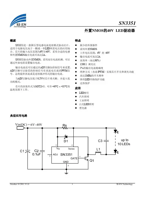
几种用于IGBT驱动的集成芯片2. 1 TLP250(TOSHIBA公司生产)在一般较低性能的三相电压源逆变器中,各种与电流相关的性能控制,通过检测直流母线上流入逆变桥的直流电流即可,如变频器中的自动转矩补偿、转差率补偿等。
同时,这一检测结果也可以用来完成对逆变单元中IGBT实现过流保护等功能。
因此在这种逆变器中,对IGBT驱动电路的要求相对比较简单,成本也比较低。
这种类型的驱动芯片主要有东芝公司生产的TLP250,夏普公司生产的PC923等等。
这里主要针对TLP250做一介绍。
TLP250包含一个GaAlAs光发射二极管和一个集成光探测器,8脚双列封装结构。
适合于IGBT或电力MOSFET栅极驱动电路。
图2为TLP250的内部结构简图,表1给出了其工作时的真值表。
TLP250的典型特征如下:1)输入阈值电流(IF):5 mA(最大);2)电源电流(ICC):11 mA(最大);3)电源电压(VCC):10~35 V;4)输出电流(IO):± 0.5 A(最小);5)开关时间(tPLH /tPHL):0.5 μ s(最大);6)隔离电压:2500 Vpms(最小)。
表2给出了TLP250的开关特性,表3给出了TLP250的推荐工作条件。
注:使用TLP250时应在管脚8和5间连接一个0.1 μ F的陶瓷电容来稳定高增益线性放大器的工作,提供的旁路作用失效会损坏开关性能,电容和光耦之间的引线长度不应超过 1 cm。
图3和图4给出了TLP250的两种典型的应用电路。
在图4中,TR1和TR2的选取与用于IGBT驱动的栅极电阻有直接的关系,例如,电源电压为24V时,TR1和TR2的Icmax≥ 24/Rg。
图5给出了TLP250驱动IGBT时,1 200 V/200 A的IGBT上电流的实验波形(50 A/10 μ s)。
可以看出,由于TLP250不具备过流保护功能,当IGBT过流时,通过控制信号关断IGBT,IGBT中电流的下降很陡,且有一个反向的冲击。
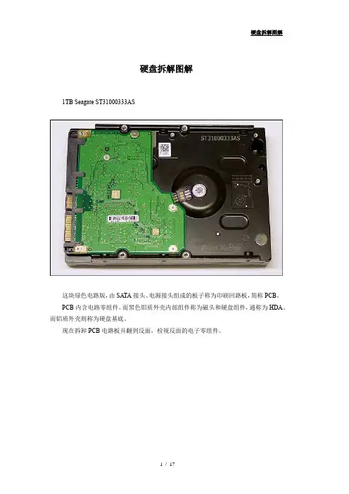
硬盘拆解图解1TB Seagate ST31000333AS这块绿色电路版,由SATA接头、电源接头组成的板子称为印刷回路板,简称PCB。
PCB内含电路零组件。
而黑色铝质外壳内部组件称为磁头和硬盘组件,通称为HDA。
而铝质外壳则称为硬盘基底。
现在拆卸PCB电路板并翻到反面,检视反面的电子零组件。
MCU控制器硬盘PCB上最大控制器为MCU (Micro Controller Unit),MCU主要功能:1、计算读写通道A/D,D/A2、掌控全盘硬盘运作状况。
3、MCU 另担当的Protocol 与控制器间的转换。
DDR DRAMDDR DRAM 32MB ,实际上32MB Cache 部份会被硬盘挪用放入硬盘运作程序。
前言已叙述,硬盘如同一个embedded system 。
需要加载OS运作。
VCM控制器下一个芯片是V oice Coil Motor controller,通称VCM控制器。
这是PCB板上最耗电的芯片,VCM控制器控制电机马达的转动及磁头移动及定位,VCM控制器可在高达工作温度Flash芯片Flash芯片储存部分的硬盘韧体与模块在盘片上位置DATA ,当你通电启动硬盘时,MCU芯片会读取Flash芯片内的数据到内存内并且开始编码。
如果缺少了这样的步骤,硬盘无法运转。
有时候,某些厂牌的硬盘PCB板上并没有Flash芯片,这表示原本Flash 芯片内的数据已存在MCU芯片内了。
震动传感器震动传感器可以感应硬盘多余的震动并且传送讯号给VCM控制器,VCM控制器接受讯号以后马上停止并复位磁头,在某些情况下,甚至会停止盘片转动,这个理论上会保护硬盘免于受损,但是实际上并无法达成保护的目的,所以请好好保护硬盘,别摔落、碰撞!在某些硬盘中,震动传感器可以感测轻微振动,而VCM控制器可以藉由震动传感器传送的讯号调整磁头的运动,这样的硬盘通常都会配有两组以上的震动传感器。
二级体另外一个保护的零组件是瞬态电压抑制二极管(Transient Voltage Suppression diode)或简称为TVS二极管。
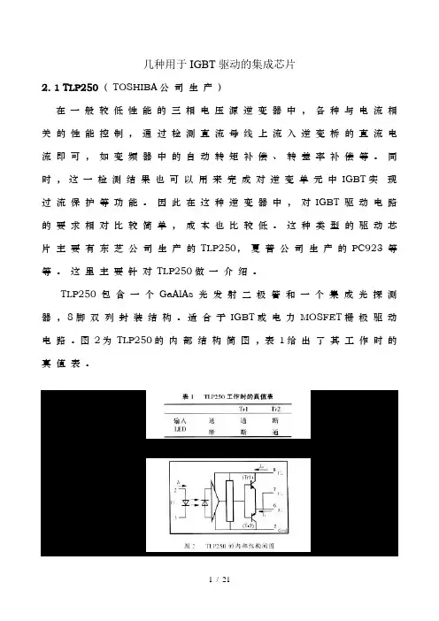
几种用于IGBT驱动的集成芯片2. 1 TLP250(TOSHIBA公司生产)在一般较低性能的三相电压源逆变器中,各种与电流相关的性能控制,通过检测直流母线上流入逆变桥的直流电流即可,如变频器中的自动转矩补偿、转差率补偿等。
同时,这一检测结果也可以用来完成对逆变单元中IGBT实现过流保护等功能。
因此在这种逆变器中,对IGBT驱动电路的要求相对比较简单,成本也比较低。
这种类型的驱动芯片主要有东芝公司生产的TLP250,夏普公司生产的PC923等等。
这里主要针对TLP250做一介绍。
TLP250包含一个GaAlAs光发射二极管和一个集成光探测器,8脚双列封装结构。
适合于IGBT或电力MOSFET栅极驱动电路。
图2为TLP250的内部结构简图,表1给出了其工作时的真值表。
TLP250的典型特征如下:1)输入阈值电流(IF):5 mA(最大);2)电源电流(ICC):11 mA(最大);3)电源电压(VCC):10~35 V;4)输出电流(IO):± 0.5 A(最小);5)开关时间(tPLH /tPHL):0.5 μ s(最大);6)隔离电压:2500 Vpms(最小)。
表2给出了TLP250的开关特性,表3给出了TLP250的推荐工作条件。
注:使用TLP250时应在管脚8和5间连接一个0.1 μ F的陶瓷电容来稳定高增益线性放大器的工作,提供的旁路作用失效会损坏开关性能,电容和光耦之间的引线长度不应超过1 cm。
图3和图4给出了TLP250的两种典型的应用电路。
在图4中,TR1和TR2的选取与用于IGBT驱动的栅极电阻有直接的关系,例如,电源电压为24V时,TR1和TR2的Icmax≥ 24/Rg。
图5给出了TLP250驱动IGBT时,1 200 V/200 A的IGBT上电流的实验波形(50 A/10 μ s)。
可以看出,由于TLP250不具备过流保护功能,当IGBT过流时,通过控制信号关断IGBT,IGBT中电流的下降很陡,且有一个反向的冲击。
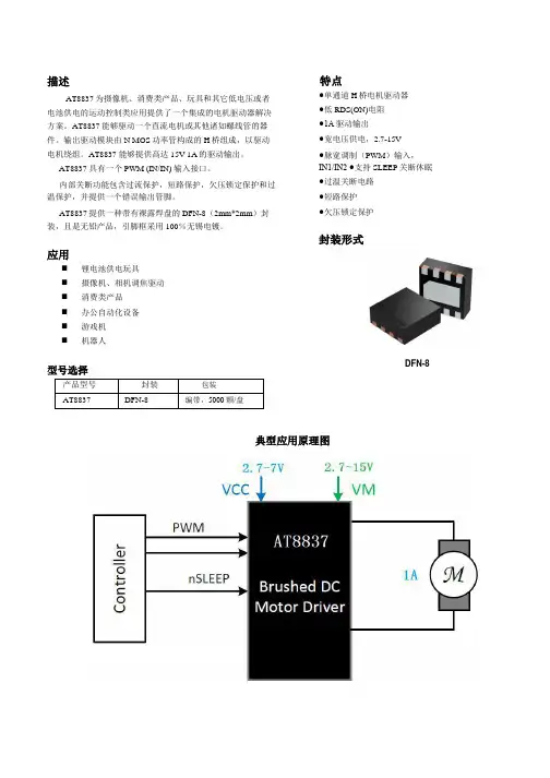
描述AT8837为摄像机、消费类产品、玩具和其它低电压或者电池供电的运动控制类应用提供了一个集成的电机驱动器解决方案。
AT8837能够驱动一个直流电机或其他诸如螺线管的器件。
输出驱动模块由N MOS功率管构成的H桥组成,以驱动电机绕组。
AT8837 能够提供高达15V 1A的驱动输出。
AT8837 具有一个PWM (IN/IN) 输入接口。
内部关断功能包含过流保护,短路保护,欠压锁定保护和过温保护,并提供一个错误输出管脚。
AT8837提供一种带有裸露焊盘的DFN-8(2mm*2mm)封装,且是无铅产品,引脚框采用100%无锡电镀。
应用⏹锂电池供电玩具⏹摄像机、相机调焦驱动⏹消费类产品⏹办公自动化设备⏹游戏机⏹机器人型号选择产品型号封装包装AT8837DFN-8编带,5000颗/盘特点●单通道H桥电机驱动器●低RDS(ON)电阻●1A驱动输出●宽电压供电,2.7-15V●脉宽调制(PWM)输入,IN1/IN2 ●支持SLEEP关断休眠●过温关断电路●短路保护●欠压锁定保护封装形式DFN-8典型应用原理图功能结构框图电特性 at Ta = 25°C, VM= 5 V,VCC=3.3V时序要求TA = 25°C, VM = 5 V, VCC = 3.3 V, RL = 20 Ω序号参数说明最小值最大值单位1t1输出使能延迟360ns2t2输出关闭延迟360ns3t3输入到输出上升延迟360ns4t4输入到输出下降延迟360ns5t5上升时间3060ns6t6下降时间3060nsSLEEP 后,芯片使能时间50us模块功能描述AT8837 为单路刷式直流电机或者螺线管提供一种集成的驱动方案。
芯片内部集成单通道 H 桥和电荷泵电路。
AT8837 提供 15V 1A 峰值输出。
简单的 PWM(IN1/IN2)接口允许简单的接口控制电路。
AT8837 还包含一个低功耗睡眠模式,允许不需要驱动芯片的时候节省功耗。
CONTINUED > 2.5-Inch HDD pg 2CONTINUED > 2.5-Inch SSD pg 3New Seagate Model Number Key, EnterpriseST 500 NM 123 1BRANDCAPACITYSEGMENTATTRIBUTESGENERATION2 letters ST = Seagate MX = Maxtor2 to 4 digits 500 = 500GB 1000 = 1000GBCapacities >9999GB:10 = 10TB 15 = 15TB2 lettersMM = Mission-Critical, 2.5-Inch, 10K MX = Mission-Critical, 2.5-Inch, 15K NM = Nearline, 3.5-Inch NX = Nearline, 2.5-Inch FM = SSD Mainstream FX = SSD Performance3 digits, non-intelligentVaries as needed, for example:Interface RPM Cache SED1 digit, intelligent 1 = 1st Generation2 = 2nd Generation3 = 3rd GenerationSeagate Partner Program MembersVisit the Sales Tools section to access the latest product roadmap, end-of-life schedule and product information. DistributorsEMEA SPP Support00-800-6890-8282US Sales Support1-800-SEAGATE or 1-405-324-4700Visit for more information or call 1-800-SEAGATE (1-800-732-4283) © 2012 Seagate Technology LLC. All rights reserved. Printed in USA. Seagate, Seagate Technology and the Wave logo are registered trademarksof Seagate Technology LLC in the United States and/or other countries. Cheetah, Constellation.2, Pulsar, Pulsar.2 and Savvio are either trademarks or registered trademarks of Seagate Technology LLC or one of its affiliated companies in the United States and/or other countries. The FIPS logo is a certification mark of NIST, which does not imply product endorsement by NIST, the U.S., or Canadian governments. All other trademarks or registered trademarks are the property of their respective owners. When referring to drive capacity, one gigabyte, or GB, equals one billion bytes and one terabyte, or TB, equals one trillion bytes. Your computer’s operating system may use a different standard of measurement and report a lower capacity. In addition, some of the listed capacity is used for formatting and other functions, and thus will not be available for data storage. Actual data rates may vary depending on operating environment and other factors. The export or re-export of hardware or software containing encryption may be regulated by the U.S. Department of Commerce, Bureau of Industry and Security (for more information, visit ). Seagate reserves the right to change, without notice, product offerings or specifications. QR501.14-1202US, February 20122 Self-Encrypting Drives (SED) and FIPS 140-2 Validated drives are not available in all models or countries. May require TCG-compliant host or controller support.3 See FIPS 140-2 Level 2 Certificate at /groups/STM/cmvp/documents/140-1/1401val2010.htm#12994 Data provided is based on format at 512 bytes.View a brief training presentation on how our model number format has changed at /seagate/ModelNumber。
迅达电梯相关资料迅达电梯相关资料迅达电梯616G5、676GL5变频器维修经验------我们维修不少电梯用的变频器,发现很多故障是因为其工作环境温度高而使元件容易老化造成的,电梯变频器安装在大楼的最顶层的控制室,经常在夏天受太阳的暴晒,加上变频器本身及制动电阻的发热,使电气室内温度非常高,工作环境温度高会缩短电子元件的使用寿命~变频器在这方面更明显,所以电梯电气室在设计时除了通风问题还要注意隔热,如墙壁用空心砖,室顶多层设计,如果能配上空调机,则变频器的寿命会长很多~安装变频器的电柜在厦天如果发现其内部温度很高时,应把电柜门打开,我见过很多厂家的电柜设计实在太小了~刚好可装上变频器~而且没安装散热风扇~——维修了不少EV-ECD01-4T0150、EV-ECD01-4T0110电梯变频器,多数是烧坏制动模块APT60GF120其驱动电路~有时整流模块及充电电阻也烧坏了,本身性能不好是其主要原因,另有一个原因是运行接触器触点打火,电压波动大,所以要以经常检查这接触器,定期清洗其触点,但这个很多电梯保养公司都没有做到~——电梯艾默生变频器HTD31用户一定要小心:艾默生变频器HTD31与TD3100的外形及电路是一样的,操作面板也是这样,但如果你不小心,将TD3100面板用到HTD31变频器上,就会马上损坏HTD31变频器主板,不能修复~最惨的是日立电梯公司卖这个主板是天价,一个要6000元~因为这个机型在市面上很少,只能忍痛向其购买~我怀疑这是日立电梯公司自己设的一个陷阱,居心不良~——蒙德电梯变频器IMS-P2-4015A改为安川616G5变频器~蒙德电梯变频器IMS-P2-4015A是仿造安川616G5-15KW变频器,但软件及硬件都远远比不上,质量很不稳定,经常烧一体化模块,维修费比较高,修过的变频器更容易坏,令人非常头痛~后来我们将其改为安川616G5变频器,从此一点问题都没有,两种变频器接线差不多的,改装很简单~------电梯变频器维修实例:今天维修一台安川676GL5(L5R4013)电梯变频器,最初原因是380V/220V变压器的保护快熔FU2(600V/1.5A)烧断了(散热风扇短路引起380V/220V变压器短路),小区管理处电工没查清原因就用铜线代替FU2快熔,通电后铜线及附近电路板打火,烧熔的铜又喷到驱动板上,造成两个2BI100NC-120功率模块及驱动板损坏,100A快熔也烧断,造成重大损失。
内存SPD芯片型号:3402W、A21SC、C21SC、24LC02
台式机硬盘3.5英寸,移动硬盘2.5英寸
台式机主要硬盘厂家:Seagate WD Maxtor Samsung Hitachi Fujitsu 硬盘BIOS:25P05VP、20PFS20V、SS725VF512、ST7559207、25P10VP
Seagate(希捷)电机驱动芯片型号:SH6960B,SH6950D,SH6790A/B,SH57828, 100244097,100124439,100317176,100369972,100256186,100143434,100343137,199120018,
H99500460,H995M0405,100217347,1002222354,23400278,23400094,23400269
WD(西部数据)电机驱动芯片型号:L6283、L6256B、L6262、L6282、L6279、L6278 Maxtor(迈拓)电机驱动芯片型号:L7250E
Sansung(三星)电机驱动芯片:HA13627
硬盘不加电维修:1、更换电路板中驱动芯片2、更换BIOS 3、12V二极管击穿
注意:硬盘装好后加电,听到噶噔一声,说明硬盘寻道成功. 如果硬盘加电后听到循环噶噔..
噶噔..噶噔...或其他异响则说明硬盘磁头憋住或硬盘损坏.(但前提要排除电路板故障) 移动硬盘厂家:三星(Samsung),日立(Hitachi),富士通Fujitsu),东芝(T oshiba),希捷(Seagate),西部数据(WD)
日立(Hitachi),富士通Fujitsu)硬盘不加电:电路板中保险击穿或开路.
三星硬盘加电后嗒..嗒..嗒..的异响,说明磁头憋住了.用巧劲震动硬盘将磁头敲归位.。
面向微型硬盘写入磁头的低耗电技术
佚名
【期刊名称】《机电工程技术》
【年(卷),期】2005(34)7
【摘要】日立制作所开发出了可降低硬盘写入驱动IC耗电量的技术,并在“VLSI symposium on Cursuits”会议上做了技术发表(演讲序号为15-1)。
该技术将耗电量由过去的1W左右降低到了380mW,芯片尺寸为1mm×0.96mm,计划用于0.85英寸、1英寸及1.8英寸微型硬盘。
【总页数】1页(P8-8)
【关键词】微型硬盘;低耗电技术;磁头;面向;日立制作所;驱动IC;VLSI;芯片尺寸;耗电量
【正文语种】中文
【中图分类】TP333.35;TP368.3
【相关文献】
1.垂直写入技术预约微型硬盘未来10年的竞争力 [J], 黄继宽
2.硬盘磁头生产中的ESD防护技术 [J], 朱柱锦;陈健;朱洪雷
3.硬盘磁头研磨修复检测技术 [J], 杨合社
4.硬盘磁头与接口技术 [J], ;
5.日美重视高密度磁记录技术研究──2001年硬盘的面记录密度将达到200亿位/in~2──技术核心是采用巨磁电阻磁头和高密度记录媒体 [J], 方光旦
因版权原因,仅展示原文概要,查看原文内容请购买。
序号品牌名称板型号主芯片主芯片型号驱动 芯片型号0Plus 10E5-D4040125100L7250E 1.20Plus 10BEAGLE D4-D4040121400L7250E 1.20Plus 10040116600L7250E 1.2金钻10代040125400L7250E 1.2金钻10代040123900SH6790A 金钻10代040125300L7250E 1.2金钻10代040121300L7250E 1.2金钻10代040128000SH6790A 金钻10代040118900L7250e 1.2金钻10代040117900L7250E 1.20040116700L7250E 1.21200Ardent C5-C1040110200L7250E 1.02300ARDENT C8-C1040111300L7250E 1.23300agere ARDENT C8-C1040111300L7250E 1.24500Ardent C5-C1040111500L7250E 1.05900Poker D.7040110900L7250E 1.265900Poker D.3040105900L7250E 1.078000Poker D.5040108000L7250E 1.289000Ardent B5-C1040109000L7250E 1.09100Ardent C5-C1040110100SH6782B 10200Ardent C5-C1040110200SH6782B 11500Ardent C5-C1040111500SH6782B 122600ARDENT C9-C1040112600SH6782B 9000Ardent B5-C1040109900SH6782B 139900Ardent B5-C1040109900SH6782B 143300BEAGLE B2-D3040113300SH6785B 15219DSP 011100219PTLS2270 DB 16236DSP 011100236PTLS2270 DB 17400DSP 0040100400PTLS2270 DB 18500DSP 040100500PTLS2270 DB 191900 LUCENT 1181G 040101900PTLS2271 CZ 202300DSP 040102300SH6770C 213400DSP 040103400SH6770C 223500LUCENT 1181K 040103500SH6770C 233700DSP 040103700PTLS2271 CZ 243700DSP 040103700SH6770C 253900DSP 040103900SH6770C 264200DSP 040104200SH6770C 274900DSP 040104900SH6770C 285600POKER C.1040105600SH6770C 296000DSP 040106000SH6770C 307100POKER C.1040107100SH6770C 313700DSP 040103700SH6770C 324600DSP 040104600SH6770C 334900DSP 040104900SH6770C 345600POKER C.1040105600SH6770C 355900Poker D.3040105900SH6770C 368200Poker C.6040108200SH6770C硬盘电路板及芯片资料大全Maxtor DiamondMax Plus 9(金钻9代)Maxtor DiamondMax Plus 8(金钻8代)Maxtor (星钻)参考图片Maxtor (美钻)序号品牌名称板型号主芯片主芯片型号驱动 芯片型号参考图片3711600Poker D.8040111600SH6770C 38AS Quantum D760009GJ 101L6279 V2.439LA Quantum D760006GJ 101TDA524740LB Quantum D760006GJ 102TDA524741LD Quantum D760009GJ 103L6279 V2.442LE Quantum D760009BGJ 104AN8411SH 43VQ agere13-126576-03437OF3L6279 V2.444VQ agere13-124862-03437OD3L6279 V2.445CX Quantum 14-113271-04TDA524746LM Quantum D760006GJ 104L6264471.1无D1760WDC WD80C24IBM-1.1L6278 AC 481.1无D1760WDC WD80C24IBM-1.1L6278 1.2491.1WDC WD80C24IBM-1.1L6278 1.2501.3WDC WD70C22-GP ST-1.3L6278 1.2E 511.3WDC WD70C22-GP ST-1.3L6278 1.7E 521.3WDC WD70C22-GP ST-1.3L6282 3.2E 531.4WDC WD70C20ST-1.4L62622.6541.6WDC WD70C20ST-1.6L62622.6551.6WDC WD70C20-SW ST-1.6L6262S2.6561.8WDC WD70C20-SW ST-1.8L62622.6571.8无D1760WDC WD70C20-SW ST-1.8L6262S2.6582.0WDC WD70C23-GP ST-2.0L6262 2.6592.0WDC WD70C23-GP ST-2.0L6278 AC 602.0WDC WD70C23-GP ST-2.0L6278 1.2612.0WDC WD70C23-GP ST-2.0L6278 1.7E 622.0WDC WD70C23-GP ST-2.0L62823.2E 632.1WDC WD70C26-GP ST-2.1L6283 1.3642.3WDC WD70C23-GP ST-2.3L6262 2.6652.3WDC WD70C23-GP ST-2.3L6278 1.2662.3WDC WD70C23-GP ST-2.3L6278 AC 672.3无D1760WDC WD70C23-GP ST-2.3L6278 1.2682.3无D1760WDC WD70C23-GP ST-2.3L6278 AC 6988i5540-LFH L6278 1.2E 7088i5540-LFH L6278 1.7E 7188i5540-LFH L6278 1.7E 7288i5540-LFH L6278 1.2E 7388i5540-LFH L6278 1.7E 7488i5540-LFH L6278 1.7E 7588i5540-LFH L6278 1.7E 7688i5540-LFH L6283 1.377SAB-M3040-HT L6278 AC 78酷鱼2ST 23400455-10623400269-02179酷鱼4ST 10016766910015819280酷鱼4ST 2340036110015819281酷鱼4ST 23400361SH6950 D 82酷鱼4ST 10017297910015819283酷鱼4BGA 100187898SH6950 D 84U4SIEMENS SAB-M3002-8D 23400278-00285U5ST 2340036123400269-021Quantum (昆腾)WestDigtal (西数)(美钻)新款WestDigtal (西数)2061-001130-300AD XW 1N16无2M 内存 Infineon 2061-001130-390AE XW 1N232061-001130-390AED7 XW 1N272061-001130-300AE XW 1N222061-001130-000AC XW 1Y032061-001130-300AE XW 1N222061-001130-300AD XC 1N162061-001130-300AD XC 1N16Seagate (希捷)86U5ST 23400361SH6950 C 87U6ST 2340036110014343488U6ST 10017297910014343489U6ST 10016766910014343490Ux ST 10022478210022235491Ux agere 10023067110022235492Ux ST 或agere 10025713310025618693Ux agere 10024903310025618694酷鱼5ST 100226836SH6950 D 95酷鱼5agere 100226836SH6950 D 96酷鱼5ST 10022683610021734797酷鱼5agere 10022683610021734798酷鱼6ST/agere 100252820100244097酷鱼6ST/agere 100252820SH6950D 酷鱼6agere 100235292SH6950D 99酷鱼6agere 100226838SH6950D 100酷鱼7ST 100274360SH6950 D 101酷鱼7agere 100274360-74SH6950 D 102酷鱼7agere 100274360-74100244097103酷鱼7agere 100319396SH6950 D 104酷鱼7agere 100319396100244097105酷鱼7ST 100252820100244097106酷鱼7agere 100252820SH6950 D 1073204AT CIRRUS LOGIC 450E-A3HAI36271083204AH CIRRUS LOGIC 450E-A4HAI362710907N9085三菱50P0278TLS2255内存 2M 11007N6054三菱90G2950TLS2254内存 2M 11107N6407三菱90G2243TLS2254贴片内存 2M 11207N6624三菱90G3198TLS2254贴片内存 2M 11307N6625三菱90G2951TLS2254内存 2M 11407N6626三菱90G2950TLS2254内存 2M 11507N5176三菱90G2950TLS2254内存 2M 11607N5686三菱90G2243TLS2254内存 2M 11707N5688三菱90G2243TLS2254内存 2M 11807N5886三菱90G2243TLS2254贴片内存 2M 11907N5887三菱90G2243TLS2254贴片内存 2M 12025L1273三菱90G0270TLS2245 6.44G 12125L1274三菱20H2978TLS2245 4.32G 12225L2496三菱90G1325TLS2245 6.44G 12325L2542三菱90G1325TLS2245 4.32G 12403L3009三菱20H2978TLS2245 6.44G 12508K0310三菱07N9803TLS2255内存 8M 12608K1801三菱08K0672TLS2255内存 8M 12708K1802三菱08K0672TLS2255内存 8M 12808K2805三菱08K2803TLS2291内存 8M 12908K1836三菱08K0672TLS2291内存 8M(希捷)Seagate(希捷)富士通IBM 笔记本笔记本08K281108K2769TLS2255上海盘夫数据恢复中心 地址:上海市长宁区武夷路697号玉溪商务中心409室 邮编:200051网址:/ 邮箱:datarecovery@ 电话:021-********。
(产品管理)HUS磁盘阵列产品说明HitachiUnifiedStorage(HUS)日立统一存储产品介绍日立数据系统有限公司2020年8月目录一. 概述1二. HDS HUS 100技术的技术优势42.1统一存储42.2独特的动态虚拟控制器和自动负载均衡7 2.3系统架构和硬件增强92.4软件增强部分112.5面向服务优化的系统132.6高安全性24×7运行保障132.7海量容量扩展和灵活的容量管理182.8SAN环境下的性能优化232.9安全简便的系统管理252.10HUS与VMW ARE的紧密结合27三. HDS HUS 100产品技术指标453.1HUS110453.2HUS130483.3HUS15050四. HDS HUS 100突出优势544.1对磁盘系统的选型依据544.2HDS HUS存储产品的突出优势55五. HUS场地准备要求565.1HUS110场地环境说明565.2HUS130场地环境说明605.3HUS150场地环境说明64一.概述日立数据解决方案价值定位今天的数据中心,除了需要面对数据量的急剧增长以及存储基础架构的复杂性之外,如何在统一存储架构中支持多种数据(块数据、文件数据、对象数据)的综合存储需求也是目前大部分企业普遍面临的问题,企业需要在满足传统的高可用性、性能、可扩展性之外,能够从容应对管理、运维以及SLO要求。
HitachiDataSystems非常了解企业面临的这些挑战,因此开发了服务导向型存储方法,使应用和业务要求能够与存储属性协调一致。
HitachiDataSystems推出了HitachiUnifiedStorage100系列存储,以模块化的方式经济高效地为大中型企业提供高效、高可靠的统一存储解决方案。
HitachiUnifiedStorage(HUS)100产品家族是HDS中端产品线新一代产品,作为广受欢迎的AMS2000系列的继任者,HUS产品线继承了HDS产品一贯的可靠性、高性能以及无瓶颈的整体优化设计。
目录第一章硬盘的物理结构和原理第二章硬盘的基本参数第三章硬盘逻辑结构简介第四章硬盘的物理安装第五章系统启动过程第六章硬盘的品牌第七章硬盘电路板测试及维修技巧第八章常用维修软件第九章专业维修软件PC3000第十章数据恢复第十一章典型故障及维修流程第一章硬盘的物理结构和原理一、引言自1956年IBM推出第一台硬盘驱动器IBM RAMAC 350至今已有四十多年了,其间虽没有CPU那种令人眼花缭乱的高速发展与技术飞跃,但我们也确实看到,在这几十年里,硬盘驱动器从控制技术、接口标准、机械结构等方面都进行了一系列改进。
正是这一系列技术上的研究与突破,使我们今天终于用上了容量更大、体积更小、速度更快、性能更可靠、价格更便宜的硬盘。
如今,虽然号称新一代驱动器的JAZ、DVD-ROM、DVD-RAM、CD-RW、MO、PD等纷纷登陆大容量驱动器市场,但硬盘以其容量大、体积小、速度快、价格便宜等优点,依然当之无愧地成为桌面电脑最主要的外部存储器,也是我们每一台PC必不可少的配置之一。
二、硬盘磁头技术1、磁头磁头是硬盘中最昂贵的部件,也是硬盘技术中最重要和最关键的一环。
传统的磁头是读写合一的电磁感应式磁头,但是,硬盘的读、写却是两种截然不同的操作,为此,这种二合一磁头在设计时必须要同时兼顾到读/写两种特性,从而造成了硬盘设计上的局限。
而MR磁头(Magnetoresistive heads),即磁阻磁头,采用的是分离式的磁头结构:写入磁头仍采用传统的磁感应磁头(MR磁头不能进行写操作),读取磁头则采用新型的MR磁头,即所谓的感应写、磁阻读。
这样,在设计时就可以针对两者的不同特性分别进行优化,以得到最好的读/写性能。
另外,MR磁头是通过阻值变化而不是电流变化去感应信号幅度,因而对信号变化相当敏感,读取数据的准确性也相应提高。
而且由于读取的信号幅度与磁道宽度无关,故磁道可以做得很窄,从而提高了盘片密度,达到200MB/英寸2,而使用传统的磁头只能达到20MB/英寸2,这也是MR磁头被广泛应用的最主要原因。
五、 推荐工作条件(Ta=25℃)
参数符号参数值单位
电源电压VCC 2.2~7.6 V 控制输入电压VIN 0~VCC V
正、反转输出电流Iout -1500~1500 mA 六、 电气特性(Ta=25℃,VCC=3V,RL=15Ω,特殊说明除外。
)
参数符号测试条件最小值典型值最大值单位整体线路
电路关断电流ICCST INA=INB=1 — 0 10 uA
工作电流ICC INA=H, INB=L or
INA=L, INB=H or
INA=H, INB=H
— 0.3 1 mA
控制输入
高电平输入电压VINH 2.0 — — V 低电平输入电压VINL — — 0.8 V 高电平输入电流IINH VIN=3V — 5 20 uA 低电平输入电流IINL VIN=0V -1 0 — uA 下拉电阻RIN — 1.5 — MΩ 驱动
输出导通阻抗RON Io=±200mA — 1 1.6 Ω 七、 输入/输出逻辑表
输入输出
INA INB OUTA OUTB
方式L L Hi-Z Hi-Z 待命状态
H L H L 前进
L H L H 后退
H H L L 刹车
TC118 单通道直流马达驱动器
十一、 封装尺寸图
DIP-8
SOP-8
深圳市雄方科技有限公司。
HA13631TCD-ROM Combo DriverADE-207-320 (Z)1st EditionFeb. 2000 DescriptionThe HA13631T is combination of Spindle, Forcus, Tracking, Slide, Tray designed for CD-ROM and have following functions and features.Functions• 1.5 A spindle driver• 0.75 A focus driver• 0.75 A tracking driver• 1.0 A slide driver• 0.75 A tray driver• Over temperature shut down (OTSD)Features• Corresponds to both of sensor motor and sensorless motor• All direct PWM drive• Low on resistance• Low power dissipation• Small thin surface mount packageHA13631TPin Arrangement2HA13631T Pin DescriptionPin No.Pin Name Function1ASGND Actuator small signal GND2SLDIN SLD driver control input3OP3IN Inverted input of OP amp. 3 for SLD driver control4OP4IN Inverted input of OP amp. 4 for TRY driver control5VSLD SLD driver power supply6TRYIN TRY driver control input7SLDP SLD driver P output8SLDN SLD driver N output9SLDGND SLD and TRY driver GND10VTRY TRY driver power supply11TRYP TRY driver P output12TRYN TRY driver N output13BSTGND Booster GND14BP1Booster pumping capacitor connection15BP2Booster pumping capacitor connection16VBST Booster output pin. This circuit generates a voltage about two times of the VSPNpin.17U U phase output18RNF SPN driver current detection19V V phase output20W W phase output21EXTCOM COMM signal on/off control and FGOUT switching. (Refer to the Timing Chart)22FGOUT FG output (Refer to the Timing Chart) open drain23COMM Start-up clock input pin for sensorless (Refer to the Timing Chart)24BRKSEL To select the brake mode (Refer to the Truth Table)25CE Chip enable (Refer to the Truth Table)26HB Hall bias switch27HU+U-phase Hall +input, and U-phase B-EMF connection pin for sensorless28ASGND Actuator small signal GND29ASGND Actuator small signal GND30VSPN SPN driver power supply31HU–U-phase Hall –input, and center tap connection pin for sensorless32HV+V-phase Hall +input, and V-phase B-EMF connection pin for sensorless33HV–V-phase Hall –input, and center tap connection pin for sensorless3HA13631TPin Description (cont)Pin No.Pin Name Function34HW+W-phase Hall +input, and W-phase B-EMF connection pin for sensorless35HW–W-phase Hall –input, and center tap connection pin for sensorless36VCTL SPN driver control input37REFIN Reference voltage for control inputs. Common to all drivers.38RT Reference voltage. The IC’s internal reference current is determined by thisvoltage and the external resistor Rt.39CT1Time constant for clock oscillation. The oscillator frequency is determined by the external capacitor and resistor Ct1 and Rt.40CT2Time constant for PWM carrier. The amplitude is determined by the value of the external capacitor Ct1.41PWMDC Phase compensation connection pin for matching PWM carrier DC level withREFIN42SGND SPN small signal GND43VSS Control block power supply. 5 V44OP2IN Inverted input of OP amp. 2 for TRK driver control45TRKIN TRK driver control input46TRKN TRK driver N output47TRKP TRK driver P output48FCSGND FCS and TRK driver GND49VFCS FCS driver power supply50FCSP FCS driver P output51FCSN FCS driver N output52FCSN FCS driver control input53OP1IN Inverted input of OP amp. 1 for FCS driver control54NC No connection55NC No connection56ASGND Actuator small signal GND4HA13631T Block Diagram5HA13631T Timing Chart 1.Start-up6HA13631T 2.Acceleration7HA13631T 3.Running8HA13631T9Truth TableTable 1CE and BRKSELCE BRKSEL SPN Driver FCS Driver TRK Driver SLD Driver TRY Driver L L Z Z Z Z Z H Enable *2Enable Enable Z Enable HL Enable *3Enable Enable Enable Z HEnable *2EnableEnableEnableZNotes: 1.Z: Hi impedance2.Short brake mode3.Reverse brake modeTable 2EXTCOM and COMMEXTCOM COMM T1~T6Mask T7~Mask FGOUT (@P = 12)LogicL L OFF Internal 6 cycle/rotationCorresponds to sensor H OFF Internal Corresponds to sensorlessHL ON Internal 36 pulse/rotation HONExternalHA13631T Application10External ComponentsParts No.ReccomendedValueReccomendedRange Purpose NoteR101a~d 2.4 kΩ≤ 22 kΩFilter resistor and atenuation for B-EMF1R102a~d7.5 kΩ≤ 22 kΩFilter resistor and atenuation for B-EMF1R103, R104—≤ 220 kΩfor FCS driver gain settingR105, R106—≤ 220 kΩfor TRK driver gain settingR107, R108—≤ 220 kΩfor SLD driver gain settingR109, R110—≤ 220 kΩfor TRY driver gain setting5 Rnf0.25 Ω≥ 0.25 ΩSPN driver current detection resistor2 Rt 6.8 kΩ≥ 5 kΩReference current settingC101—≥ 0.1 µF for Power supply by passingC1020.1 µF—for Booster pumpingC1030.47 µF—for Booster output smoothingC1042200 pF—for PWM carrier oscillation DC level adjustmentC105a~d0.1 µF—for B-EMF filter1 Ct1100 pF—Time constant for CLK oscillation3, 4 Ct2400 pF—PWM carrier generation time constant3, 4 Notes: 1.The values of R101a~d, R102a~d, and C105a~d are determined by the following equation.Where,Nomax: Maximum rotation speed (rpm)P: Number of spindle motor poles (Total number of S poles and N poles)R101 R10214≥(at Vspn = 5 V)11Nomax P1R101x1R102xC105x =+2.The output current maximum value Iospnmax of SPN driver is controlled according to thefollowing equation. However, Vspncl is the current limiter reference voltage. (See the electrical characteristics)Iospnmax =Vspncl Rnf3.The CLK oscillation frequency fclk and Rt1 ⋅ Ct1 are related by the following equation.Vrt2 Ct1 Rt (Vct1h − Vct1l)fclk =Where,Vrt: RT pin voltage (See the electrical characteristics)Vct1h: CT1 pin high voltage (See the electrical characteristics)Vct1l: CT1 pin low voltage (See the electrical characteristics)4.The PWM carrier frequency fpwm and the amplitude Apwm are determined by the followingequation.fpwm =Vrt8 Ct1 Rt (Vct1h − Vct1l)Apwm =(Vct1h − Vct1l)4 Ct1Ct2However, Ct2 = 4 Ct15.As 5 k Ω appears as an internal resistance at TRYIN (pin 6), caution is required when markingthe gain setting.Absolute Maximum Ratings (Ta = 25°C)Item Symbol Rating Unit Note Control block supply voltage Vss7V1SPN supply voltage Vspn7V1FCS & TRK supply voltage Vfcs9.5V1SLD supply voltage Vsld7V1TRY supply voltage Vtry9.5V1Input voltage Vin0 to Vss V2SPN output current Iospn 1.5 (2.5)A3FCS output current Iofcs0.75 (1.5)A3TRK output current Iotrk0.75 (1.5)A3SLD output current Iosld 1.0 (1.5)A3TRY output current Iotry0.75 (1.5)A3Power dissipation Pt 2.5W4 Junction temperature Tj150°C1 Storage temperature range Tstg–55 to +125°CNote: 1.Operating range is shown below.Vss = 4.5 to 5.5 V, Vspn = 4.25 to 5.75 V, Vfcs = 4.25 to 8.5 V, Vsld = 4.25 to 5.75 V, Vtry = 4.25to 8.5 V, Tjopr = –20 to +135°CWhen operating with Vfcs > Vss, it is necessary to set Vtry = Vfcs. Also, settings must be madethat satisfy the following condition:Vtry + Vss – Vsld ≤ 8.5 V2.Applied to analog and logic input.3.Values in parentheses are peak values. ASO (Area of Safety Operation) is shown below.4.Thermal resistance is shown below.θj-tab ≤ 6°C/W (back side tab soldering area is 70% or more)θj-a1 ≤ 30°C/W (mounted on 4 layer glass-epoxy board, back side tab soldering area is 70% ormore)(Ta = 25°C, Vss = 5 V, Vspn = 12 V, Vfcs = 5 V, Vsld = 12 V)Item Symbol Min Typ Max Unit Test Conditions ApplicablePins NoteQuiescent current Iss0—0.20.5mA CE = L VSSIspn0—0.10.2mA VSPNIfcs0——0.1mA VFCSIsld0——0.1mA VSLDItry0——0.1mA VTRYIss1—2535mA CE = H VSSIspn1—— 1.0mA All load open VSPNIfcs1—— 1.0mA VFCSIsld1—— 1.0mA VSLDItry1— 4.0 6.0mA VTRYLogic Input current Iin——±10µA Vin = 0 to Vss EXTCOM, input Low level voltage Vil——0.8V COMM,High level voltage Vih 2.0——V BRKSEL,CELogic Low level voltage Vol—0.20.4V Io = 1 mA FGOUToutput 1Leakage current ICER 1——±10µA VCE= 5.5 VLogic Low level voltage Vol—0.30.6V Io = 15 mA HBoutput 2Leakage current ICER 1— 1.2 1.5µA VCE= 5.5 VSPN driver Output onresistanceRonspn— 1.2 1.5ΩIo = 1.0 A U, V, W1 Leakage current Ioffspn——±100µA Vspn = 15 VSlew rate SRspn—60—V/µs Load open5 Current limitervoltageVspncl—0.25±10%V Rnf = 0.25 ΩRNFFCS/ TRK Output onresistanceRonfcs— 3.0 3.75ΩIo = 0.5 A FCSP/N,TRKP/N1driver Leakage current Iofffcs——±100µA Vfcs = 15 VSlew rate SRfcs—60—V/µs Load open5SLD driver Output onresistanceRonsld— 2.0 2.5ΩIo = 1.0 A SLDP/N1 Leakage current Ioffsld——±100µA Vsld = 15 VSlew rate SRsld—60—V/µs Load open5Item Symbol Min Typ Max Unit Test Conditions ApplicablePins NoteTRY driver Output onresistanceRontry— 3.0 3.75ΩIo = 0.5 A TRYP/N1 Leakage current Iofftry——±100µA Vtry = 15 VSlew rate SRtry—125—V/µs Load open5CLK RT voltage Vrt— 1.37±5%V RT OSC CT1 charge current Ict1p—180±10%µA Rt = 6.8 kΩCT1CT1 dischargecurrentIct1n—–180±10%µA Rt = 6.8 kΩCT1 high voltage Vct1h— 2.7±0.1VCT1 low voltage Vct1l— 1.47±0.1VCLK oscillationfrequencyfclk—460±10%kHz Ct1 = 100 pFBias Drive frequency fbst—fclk/2—kHz BP1 Output voltage Vbst16.016.5—V Vspn = 12 V VBST9.09.5—V Vspn = 5 VPWM PWM frequency fpwm—fclk/4—kHz CT2 carrier CT2 charge current Ict2p—180±10%µA Rt = 6.8 kΩCT2 dischargecurrentIct2n—–180±10%µA Rt = 6.8 kΩDC feedbackresistanceRdc—20±20%kΩPWMDC Offset voltage Vospwm——±30mVZero cross Common modeinput voltage rangeVczd0— 4.0V HU+/–,HV+/–,detection Input voltage range Vinzd50——mVpp HW+/–Hysteresis Vhyszd111621mVppFGOUT pulse width Tmint—64/fclk±4/fclkµs FGOUTSPN Input current Ictl——±3.0µA Vctl = 0.5 to 4.5 V VCTLcontrol Dead zone voltage Vdzctl±50—±200mV2REFIN voltagerangeVref 1.0— 2.65V REFIN4Control gain Dspn119139159%/V Ct2 = 680 pF,Ct1 = 100 pFU, V, W2Item Symbol Min Typ Max Unit Test Conditions ApplicablePins NoteOP1~Input current Iinop——±0.1µA Vin = 0 to Vss OP1~4INOP4Offset voltage Vosop——±60mV FCSIN, Open loop gain Gvolop—64—dB f = 1kHz TRKIN,5Gain bandwidth Bop— 1.6—MHz SLDIN,TRYIN5OP1~ OP3Output lowvoltageVoopl——0.5V Io = –0.2 mA FCSIN,TRKIN, Output highvoltageVooph Vss–1.0——V Io = 0.2 mA SLDINOP4Output lowvoltageVoopl——0.5V Io = –0.03 mA TRYINOutput high voltage Vooph Vss–1.7——V Io = 0.03 mAFCS/ TRK/Quiescent offset duty Dqfcs——±2%FCS/TRK/SLD/TRYIN = REFINFCSP/N,TRKP/N,3SLD/ TRY control Control gain Dfcs636873%/V Ct2 = 680 pF,Ct1 = 100 pFSLDP/N,TRYP/NOTSD Operating temperature Tsd135180—°C5 Hysteresis Thys—80—°CNote:1.Specified by sum of the upper and lower saturation voltages.2.See figure 1. Where,Dspn =∆D ∆VctlFigure 13.See figure 2. Where, x = fcs, trk, sld, try.Dx =∆D ∆VxinFigure 24.If Vref < 1.5 V, 100% PWM duty control may not be possible.5.Design guide only.Reference DataPackage DimensionsCautions1.Hitachi neither warrants nor grants licenses of any rights of Hitachi’s or any third party’s patent,copyright, trademark, or other intellectual property rights for information contained in this document.Hitachi bears no responsibility for problems that may arise with third party’s rights, includingintellectual property rights, in connection with use of the information contained in this document.2.Products and product specifications may be subject to change without notice. Confirm that you have received the latest product standards or specifications before final design, purchase or use.3.Hitachi makes every attempt to ensure that its products are of high quality and reliability. However,contact Hitachi’s sales office before using the product in an application that demands especially high quality and reliability or where its failure or malfunction may directly threaten human life or cause risk of bodily injury, such as aerospace, aeronautics, nuclear power, combustion control, transportation,traffic, safety equipment or medical equipment for life support.4.Design your application so that the product is used within the ranges guaranteed by Hitachi particularly for maximum rating, operating supply voltage range, heat radiation characteristics, installationconditions and other characteristics. Hitachi bears no responsibility for failure or damage when used beyond the guaranteed ranges. Even within the guaranteed ranges, consider normally foreseeable failure rates or failure modes in semiconductor devices and employ systemic measures such as fail-safes, so that the equipment incorporating Hitachi product does not cause bodily injury, fire or other consequential damage due to operation of the Hitachi product.5.This product is not designed to be radiation resistant.6.No one is permitted to reproduce or duplicate, in any form, the whole or part of this document without written approval from Hitachi.7.Contact Hitachi’s sales office for any questions regarding this document or Hitachi semiconductor products.Hitachi, Ltd.Semiconductor & Integrated Circuits.Nippon Bldg., 2-6-2, Ohte-machi, Chiyoda-ku, Tokyo 100-0004, Japan Tel: Tokyo (03) 3270-2111 Fax: (03) 3270-5109Copyright ' Hitachi, Ltd., 2000. All rights reserved. Printed in Japan.Hitachi Asia Pte. Ltd.16 Collyer Quay #20-00Hitachi TowerSingapore 049318Tel: 535-2100Fax: 535-1533URLNorthAmerica : http:/Europe : /hel/ecg Asia (Singapore): .sg/grp3/sicd/index.htm Asia (Taiwan): /E/Product/SICD_Frame.htm Asia (HongKong): /eng/bo/grp3/index.htm Japan : http://www.hitachi.co.jp/Sicd/indx.htmHitachi Asia Ltd.Taipei Branch Office3F, Hung Kuo Building. No.167, Tun-Hwa North Road, Taipei (105)Tel: <886> (2) 2718-3666Fax: <886> (2) 2718-8180Hitachi Asia (Hong Kong) Ltd.Group III (Electronic Components)7/F., North Tower, World Finance Centre,Harbour City, Canton Road, Tsim Sha Tsui,Kowloon, Hong Kong Tel: <852> (2) 735 9218Fax: <852> (2) 730 0281 Telex: 40815 HITEC HXHitachi Europe Ltd.Electronic Components Group.Whitebrook ParkLower Cookham Road MaidenheadBerkshire SL6 8YA, United Kingdom Tel: <44> (1628) 585000Fax: <44> (1628) 778322Hitachi Europe GmbHElectronic components Group Dornacher Stra βe 3D-85622 Feldkirchen, Munich GermanyTel: <49> (89) 9 9180-0Fax: <49> (89) 9 29 30 00Hitachi Semiconductor (America) Inc.179 East Tasman Drive,San Jose,CA 95134 Tel: <1> (408) 433-1990Fax: <1>(408) 433-0223For further information write to:。