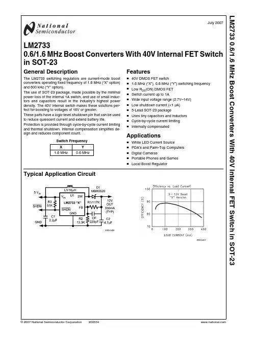
July 2007 LM27330.6/1.6 MHz Boost Converters With 40V Internal FET Switch in SOT-23General DescriptionThe LM2733 switching regulators are current-mode boost converters operating fixed frequency of 1.6 MHz (“X” option) and 600 kHz (“Y” option).The use of SOT-23 package, made possible by the minimal power loss of the internal 1A switch, and use of small induc-tors and capacitors result in the industry's highest power density. The 40V internal switch makes these solutions per-fect for boosting to voltages of 16V or greater.These parts have a logic-level shutdown pin that can be used to reduce quiescent current and extend battery life. Protection is provided through cycle-by-cycle current limiting and thermal shutdown. Internal compensation simplifies de-sign and reduces component count.Switch FrequencyX Y1.6 MHz0.6 MHz Features■40V DMOS FET switch■ 1.6 MHz (“X”), 0.6 MHz (“Y”) switching frequency ■Low R DS(ON) DMOS FET■Switch current up to 1A■Wide input voltage range (2.7V–14V)■Low shutdown current (<1 µA)■5-Lead SOT-23 package■Uses tiny capacitors and inductors■Cycle-by-cycle current limiting■Internally compensatedApplications■White LED Current Source■PDA’s and Palm-Top Computers■Digital Cameras■Portable Phones and Games■Local Boost RegulatorTypical Application Circuit2005542420055457© 2007 National Semiconductor LM2733 0.6/1.6 MHz Boost Converters With 40V Internal FET Switch in SOT-2320055401200554582005544020055459Connection DiagramTop View200554025-Lead SOT-23 PackageSee NS Package Number MF05A 2L M 2733Ordering InformationOrder Number PackageTypePackageDrawingSuppliedAsPackageIDLM2733XMFSOT23-5MF05A 1K Tapeand ReelS52ALM2733XMFX3K Tapeand ReelS52ALM2733YMF1K Tapeand ReelS52BLM2733YMFX3K Tapeand ReelS52BPin DescriptionsPin Name Function1SW Drain of the internal FET switch.2GND Analog and power ground.3FB Feedback point that connects to external resistive divider.4SHDN Shutdown control input. Connect to VINif this feature is not used.5VINAnalog and power input.LM2733Block Diagram20055403Theory of OperationThe LM2733 is a switching converter IC that operates at a fixed frequency (0.6 or 1.6 MHz) using current-mode control for fast transient response over a wide input voltage range and incorporate pulse-by-pulse current limiting protection.Because this is current mode control, a 50 m Ω sense resistor in series with the switch F ET is used to provide a voltage (which is proportional to the FET current) to both the input of the pulse width modulation (PWM) comparator and the cur-rent limit amplifier.At the beginning of each cycle, the S-R latch turns on the FET.As the current through the FET increases, a voltage (propor-tional to this current) is summed with the ramp coming from the ramp generator and then fed into the input of the PWM comparator. When this voltage exceeds the voltage on the other input (coming from the Gm amplifier), the latch resets and turns the FET off. Since the signal coming from the Gmamplifier is derived from the feedback (which samples the voltage at the output), the action of the PWM comparator constantly sets the correct peak current through the FET to keep the output volatge in regulation.Q1 and Q2 along with R3 - R6 form a bandgap voltage refer-ence used by the IC to hold the output in regulation. The currents flowing through Q1 and Q2 will be equal, and the feedback loop will adjust the regulated output to maintain this.Because of this, the regulated output is always maintained at a voltage level equal to the voltage at the FB node "multiplied up" by the ratio of the output resistive divider.The current limit comparator feeds directly into the flip-flop,that drives the switch FET. If the FET current reaches the limit threshold, the FET is turned off and the cycle terminated until the next clock pulse. The current limit input terminates the pulse regardless of the status of the output of the PWM com-parator. 4L M 2733Absolute Maximum Ratings (Note 1)If Military/Aerospace specified devices are required,please contact the National Semiconductor Sales Office/Distributors for availability and specifications.Storage Temperature Range −65°C to +150°C Operating Junction Temperature Range−40°C to +125°CLead Temp. (Soldering, 5 sec.)300°CPower Dissipation (Note 2)Internally LimitedFB Pin Voltage −0.4V to +6V SW Pin Voltage−0.4V to +40V Input Supply Voltage −0.4V to +14.5V Shutdown Input Voltage (Survival)−0.4V to +14.5VθJ-A (SOT23-5)265°C/WESD Rating (Note 3) Human Body Model Machine Model2 kV 200VElectrical CharacteristicsLimits in standard typeface are for T J = 25°C, and limits in boldface type apply over the full operating temperature range (−40°C ≤ T J ≤ +125°C). Unless otherwise specified: V IN = 5V, V SHDN = 5V, I L = 0A.Symbol ParameterConditionsMin (Note 4)Typical (Note 5)Max (Note 4)Units V IN Input Voltage 2.7 14V I SW Switch Current Limit (Note 6) 1.0 1.5 A R DS (ON)Switch ON Resistance I SW = 100 mA 500650m ΩSHDN TH Shutdown Threshold Device ON 1.5 V Device OFF 0.50I SHDN Shutdown Pin Bias Current V SHDN = 0 0 µA V SHDN = 5V 02V FB Feedback Pin Reference VoltageV IN = 3V 1.205 1.230 1.255V I FB Feedback Pin Bias Current V FB = 1.23V60 nA I QQuiescent CurrentV SHDN = 5V, Switching "X"2.13.0mA V SHDN = 5V, Switching "Y"1.12V SHDN = 5V, Not Switching 400500µA V SHDN = 00.0241FB Voltage Line Regulation2.7V ≤ V IN ≤ 14V 0.02 %/V F SWSwitching Frequency“X” Option 1.15 1.6 1.85MHz “Y” Option0.400.600.8D MAX Maximum Duty Cycle “X” Option 8793 %“Y” Option9396 I LSwitch LeakageNot Switching V SW = 5V1µANote 1:Absolute Maximum Ratings indicate limits beyond which damage to the component may occur. Electrical specifications do not apply when operating the device outside of the limits set forth under the operating ratings which specify the intended range of operating conditions.Note 2:The maximum power dissipation which can be safely dissipated for any application is a function of the maximum junction temperature, T J (MAX) = 125°C, the junction-to-ambient thermal resistance for the SOT-23 package, θJ-A = 265°C/W, and the ambient temperature, T A . The maximum allowable power dissipation at any ambient temperature for designs using this device can be calculated using the formula:If power dissipation exceeds the maximum specified above, the internal thermal protection circuitry will protect the device by reducing the output voltage as required to maintain a safe junction temperature.Note 3:The human body model is a 100 pF capacitor discharged through a 1.5 k Ω resistor into each pin. The machine model is a 200 pF capacitor discharged directly into each pin.Note 4:Limits are guaranteed by testing, statistical correlation, or design.Note 5:Typical values are derived from the mean value of a large quantity of samples tested during characterization and represent the most likely expected value of the parameter at room temperature.Note 6:Switch current limit is dependent on duty cycle (see Typical Performance Characteristics). Limits shown are for duty cycles ≤ 50%.LM2733Typical Performance CharacteristicsUnless otherwise specified: V IN = 5V, SHDN pin is tied to V IN .Iq V IN (Active) vs Temperature - "X"20055410Iq V IN (Active) vs Temperature - "Y"20055442Oscillator Frequency vs Temperature - "X"20055408Oscillator Frequency vs Temperature - "Y"20055443Max. Duty Cycle vs Temperature - "X"20055455Max. Duty Cycle vs Temperature - "Y"20055456 6L M 2733Feedback Voltage vs Temperature20055406RDS(ON) vs Temperature20055407Current Limit vs Temperature20055409RDS(ON)vs VIN20055423Efficiency vs Load Current (VOUT= 12V) - "X"20055414Efficiency vs Load Current (VOUT= 15V) - "X"20055445LM2733Efficiency vs Load Current (V OUT = 20V) - "X"20055446Efficiency vs Load Current (V OUT = 25V) - "X"20055447Efficiency vs Load Current (V OUT = 30V) - "X"20055448Efficiency vs Load Current (V OUT = 35V) - "X"20055449Efficiency vs Load Current (V OUT = 40V) - "X"20055450Efficiency vs Load (V OUT = 15V) - "Y"20055435 8L M 2733Efficiency vs Load (VOUT= 20V) - "Y"20055427Efficiency vs Load (VOUT= 25V) - "Y"20055428Efficiency vs Load (VOUT= 30V) - "Y"20055429Efficiency vs Load (VOUT= 35V) - "Y"20055430Efficiency vs Load (VOUT= 40V) - "Y"20055432 LM2733Application HintsSELECTING THE EXTERNAL CAPACITORSThe best capacitors for use with the LM2733 are multi-layer ceramic capacitors. They have the lowest ESR (equivalent series resistance) and highest resonance frequency which makes them optimum for use with high frequency switching converters.When selecting a ceramic capacitor, only X5R and X7R di-electric types should be used. Other types such as Z5U and Y5F have such severe loss of capacitance due to effects of temperature variation and applied voltage, they may provide as little as 20% of rated capacitance in many typical applica-tions. Always consult capacitor manufacturer’s data curves before selecting a capacitor. High-quality ceramic capacitors can be obtained from Taiyo-Yuden, AVX, and Murata.SELECTING THE OUTPUT CAPACITORA single ceramic capacitor of value 4.7 µF to 10 µF will provide sufficient output capacitance for most applications. For output voltages below 10V, a 10 µF capacitance is required. If larger amounts of capacitance are desired for improved line support and transient response, tantalum capacitors can be used in parallel with the ceramics. Aluminum electrolytics with ultra low ESR such as Sanyo Oscon can be used, but are usually prohibitively expensive. Typical AI electrolytic capacitors are not suitable for switching frequencies above 500 kHz due to significant ringing and temperature rise due to self-heating from ripple current. An output capacitor with excessive ESR can also reduce phase margin and cause instability.SELECTING THE INPUT CAPACITORAn input capacitor is required to serve as an energy reservoir for the current which must flow into the coil each time the switch turns ON. This capacitor must have extremely low ESR, so ceramic is the best choice. We recommend a nomi-nal value of 2.2 µF, but larger values can be used. Since this capacitor reduces the amount of voltage ripple seen at the input pin, it also reduces the amount of EMI passed back along that line to other circuitry.FEED-FORWARD COMPENSATIONAlthough internally compensated, the feed-forward capacitor Cf is required for stability (see Basic Application Circuit ).Adding this capacitor puts a zero in the loop response of the converter. Without it, the regulator loop can oscillate. The recommended frequency for the zero fz should be approxi-mately 8 kHz. Cf can be calculated using the formula:Cf = 1 / (2 X π X R1 X fz)SELECTING DIODESThe external diode used in the typical application should be a Schottky diode. If the switch voltage is less than 15V, a 20V diode such as the MBR0520 is recommended. If the switch voltage is between 15V and 25V, a 30V diode such as the MBR0530 is recommended. If the switch voltage exceeds 25V, a 40V diode such as the MBR0540 should be used.The MBR05XX series of diodes are designed to handle a maximum average current of 0.5A. For applications exceed-ing 0.5A average but less than 1A, a Microsemi UPS5817 can be used.LAYOUT HINTSHigh frequency switching regulators require very careful lay-out of components in order to get stable operation and lownoise. All components must be as close as possible to the LM2733 device. It is recommended that a 4-layer PCB be used so that internal ground planes are available.As an example, a recommended layout of components is shown:20055422Recommended PCB Component LayoutSome additional guidelines to be observed:1.Keep the path between L1, D1, and C2 extremely short.Parasitic trace inductance in series with D1 and C2 will increase noise and ringing.2.The feedback components R1, R2 and CF must be keptclose to the FB pin of U1 to prevent noise injection on the FB pin trace.3.If internal ground planes are available (recommended)use vias to connect directly to ground at pin 2 of U1, as well as the negative sides of capacitors C1 and C2.SETTING THE OUTPUT VOLTAGEThe output voltage is set using the external resistors R1 and R2 (see Basic Application Circuit ). A value of approximately 13.3 k Ω is recommended for R2 to establish a divider current of approximately 92 µA. R1 is calculated using the formula:R1 = R2 X (V OUT /1.23 − 1)SWITCHING FREQUENCYThe LM2733 is provided with two switching frequencies: the “X” version is typically 1.6 MHz, while the “Y” version is typi-cally 600 kHz. The best frequency for a specific application must be determined based on the tradeoffs involved:Higher switching frequency means the inductors and capac-itors can be made smaller and cheaper for a given output voltage and current. The down side is that efficiency is slightly lower because the fixed switching losses occur more fre-quently and become a larger percentage of total power loss.EMI is typically worse at higher switching frequencies be-cause more EMI energy will be seen in the higher frequency spectrum where most circuits are more sensitive to such in-terference. 10L M 273320055405Basic Application CircuitDUTY CYCLE The maximum duty cycle of the switching regulator deter-mines the maximum boost ratio of output-to-input voltage that the converter can attain in continuous mode of operation. The duty cycle for a given boost application is defined as:This applies for continuous mode operation.The equation shown for calculating duty cycle incorporatesterms for the FET switch voltage and diode forward voltage.The actual duty cycle measured in operation will also be af-fected slightly by other power losses in the circuit such as wirelosses in the inductor, switching losses, and capacitor ripple current losses from self-heating. Therefore, the actual (effec-tive) duty cycle measured may be slightly higher than calcu-lated to compensate for these power losses. A good approximation for effctive duty cycle is :DC (eff) = (1 - Efficiency x (V IN /V OUT ))Where the efficiency can be approximated from the curves provided.INDUCTANCE VALUEThe first question we are usually asked is: “How small can I make the inductor?” (because they are the largest sized com-ponent and usually the most costly). The answer is not simple and involves tradeoffs in performance. Larger inductors mean less inductor ripple current, which typically means less output voltage ripple (for a given size of output capacitor). Larger inductors also mean more load power can be delivered be-cause the energy stored during each switching cycle is:E =L/2 X (lp)2Where “lp” is the peak inductor current. An important point to observe is that the LM2733 will limit its switch current based on peak current. This means that since lp(max) is fixed, in-creasing L will increase the maximum amount of power avail-able to the load. Conversely, using too little inductance may limit the amount of load current which can be drawn from the output.Best performance is usually obtained when the converter is operated in “continuous” mode at the load current range of interest, typically giving better load regulation and less output ripple. Continuous operation is defined as not allowing the in-ductor current to drop to zero during the cycle. It should be noted that all boost converters shift over to discontinuous op-eration as the output load is reduced far enough, but a larger inductor stays “continuous” over a wider load current range.To better understand these tradeoffs, a typical application cir-cuit (5V to 12V boost with a 10 µH inductor) will be analyzed.We will assume:V IN = 5V, V OUT = 12V, V DIODE = 0.5V, V SW = 0.5V Since the frequency is 1.6 MHz (nominal), the period is ap-proximately 0.625 µs. The duty cycle will be 62.5%, whichmeans the ON time of the switch is 0.390 µs. It should be noted that when the switch is ON, the voltage across the in-ductor is approximately ing the equation:V = L (di/dt)We can then calculate the di/dt rate of the inductor which isfound to be 0.45 A/µs during the ON time. Using these facts,we can then show what the inductor current will look like dur-ing operation:2005541210 µH Inductor Current,5V–12V Boost (LM2733X)During the 0.390 µs ON time, the inductor current ramps up 0.176A and ramps down an equal amount during the OFF time. This is defined as the inductor “ripple current”. It can also be seen that if the load current drops to about 33 mA, the inductor current will begin touching the zero axis which means it will be in discontinuous mode. A similar analysis can be performed on any boost converter, to make sure the ripple current is reasonable and continuous operation will be main-tained at the typical load current values.MAXIMUM SWITCH CURRENTThe maximum FET swtch current available before the current limiter cuts in is dependent on duty cycle of the application.This is illustrated in the graphs below which show both the typical and guaranteed values of switch current for both the "X" and "Y" versions as a function of effective (actual) duty cycle:LM273320055425Switch Current Limit vs Duty Cycle - "X"20055426Switch Current Limit vs Duty Cycle - "Y"CALCULATING LOAD CURRENTAs shown in the figure which depicts inductor current, the load current is related to the average inductor current by the rela-tion:I LOAD = I IND (AVG) x (1 - DC)Where "DC" is the duty cycle of the application. The switch current can be found by:I SW = I IND (AVG) + ½ (I RIPPLE )Inductor ripple current is dependent on inductance, duty cy-cle, input voltage and frequency:I RIPPLE = DC x (V IN -V SW ) / (f x L)combining all terms, we can develop an expression which al-lows the maximum available load current to be calculated:The equation shown to calculate maximum load current takes into account the losses in the inductor or turn-OFF switching losses of the FET and diode. For actual load current in typical applications, we took bench data for various input and output voltages for both the "X" and "Y" versions of the LM2733 anddisplayed the maximum load current available for a typical device in graph form:20055434Max. Load Current vs V IN - "X"20055433Max. Load Current vs V IN - "Y"DESIGN PARAMETERS V SW AND I SWThe value of the FET "ON" voltage (referred to as V SW in the equations) is dependent on load current. A good approxima-tion can be obtained by multiplying the "ON Resistance" of the FET times the average inductor current.FET on resistance increases at V IN values below 5V, since the internal N-FET has less gate voltage in this input voltage range (see Typical performance Characteristics curves).Above V IN = 5V, the FET gate voltage is internally clamped to 5V.The maximum peak switch current the device can deliver is dependent on duty cycle. The minimum value is guaranteed to be > 1A at duty cycle below 50%. For higher duty cycles,see Typical performance Characteristics curves.THERMAL CONSIDERATIONSAt higher duty cycles, the increased ON time of the F ET means the maximum output current will be determined by power dissipation within the LM2733 FET switch. The switch power dissipation from ON-state conduction is calculated by:P (SW) = DC x I IND (AVE)2 x R DS ON12L M 2733There will be some switching losses as well, so some derating needs to be applied when calculating IC power dissipation.MINIMUM INDUCTANCEIn some applications where the maximum load current is rel-atively small, it may be advantageous to use the smallest possible inductance value for cost and size savings. The con-verter will operate in discontinuous mode in such a case.The minimum inductance should be selected such that the inductor (switch) current peak on each cycle does not reach the 1A current limit maximum. To understand how to do this,an example will be presented.In the example, the LM2733X will be used (nominal switching frequency 1.6 MHz, minimum switching frequency 1.15 MHz). This means the maximum cycle period is the re-ciprocal of the minimum frequency:T ON(max) = 1/1.15M = 0.870 µsWe will assume the input voltage is 5V, V OUT = 12V, V SW =0.2V, V DIODE = 0.3V. The duty cycle is:Duty Cycle = 60.3%Therefore, the maximum switch ON time is 0.524 µs. An in-ductor should be selected with enough inductance to prevent the switch current from reaching 1A in the 0.524 µs ON time interval (see below):20055413Discontinuous Design, 5V–12V Boost (LM2733X)The voltage across the inductor during ON time is 4.8V. Min-imum inductance value is found by:V = L X dl/dt, L = V X (dt/dl) = 4.8 (0.524µ/1) = 2.5 µH In this case, a 2.7 µH inductor could be used assuming it pro-vided at least that much inductance up to the 1A current value.This same analysis can be used to find the minimum induc-tance for any boost application. Using the slower switching “Y” version requires a higher amount of minimum inductance because of the longer switching period.INDUCTOR SUPPLIERSSome of the recommended suppliers of inductors for this product include, but not limited to are Sumida, Coilcraft, Pana-sonic, TDK and Murata. When selecting an inductor, make certain that the continuous current rating is high enough to avoid saturation at peak currents. A suitable core type must be used to minimize core (switching) losses, and wire power losses must be considered when selecting the current rating.SHUTDOWN PIN OPERATIONThe device is turned off by pulling the shutdown pin low. If this function is not going to be used, the pin should be tied directly to V IN . If the SHDN function will be needed, a pull-up resistor must be used to V IN (approximately 50k-100k Ω recommend-ed). The SHDN pin must not be left unterminated.LM2733Physical Dimensions inches (millimeters) unless otherwise noted5-Lead SOT-23 PackageOrder Number LM2733XMF, LM2733XMFX, LM2733YMF or LM2733YMFXNS Package Number MF05A 14L M 2733LM2733 NotesNotesL M 2733 0.6/1.6 M H z B o o s t C o n v e r t e r s W i t h 40V I n t e r n a l F E T S w i t c h i n S O T -23THE CONTENTS OF THIS DOCUMENT ARE PROVIDED IN CONNECTION WITH NATIONAL SEMICONDUCTOR CORPORATION (“NATIONAL”) PRODUCTS. NATIONAL MAKES NO REPRESENTATIONS OR WARRANTIES WITH RESPECT TO THE ACCURACY OR COMPLETENESS OF THE CONTENTS OF THIS PUBLICATION AND RESERVES THE RIGHT TO MAKE CHANGES TO SPECIF ICATIONS AND PRODUCT DESCRIPTIONS AT ANY TIME WITHOUT NOTICE. NO LICENSE, WHETHER EXPRESS,IMPLIED, ARISING BY ESTOPPEL OR OTHERWISE, TO ANY INTELLECTUAL PROPERTY RIGHTS IS GRANTED BY THIS DOCUMENT.TESTING AND OTHER QUALITY CONTROLS ARE USED TO THE EXTENT NATIONAL DEEMS NECESSARY TO SUPPORT NATIONAL’S PRODUCT WARRANTY. EXCEPT WHERE MANDATED BY GOVERNMENT REQUIREMENTS, TESTING OF ALL PARAMETERS OF EACH PRODUCT IS NOT NECESSARILY PERF ORMED. NATIONAL ASSUMES NO LIABILITY F OR APPLICATIONS ASSISTANCE OR BUYER PRODUCT DESIGN. BUYERS ARE RESPONSIBLE F OR THEIR PRODUCTS AND APPLICATIONS USING NATIONAL COMPONENTS. PRIOR TO USING OR DISTRIBUTING ANY PRODUCTS THAT INCLUDE NATIONAL COMPONENTS, BUYERS SHOULD PROVIDE ADEQUATE DESIGN, TESTING AND OPERATING SAFEGUARDS.EXCEPT AS PROVIDED IN NATIONAL’S TERMS AND CONDITIONS OF SALE FOR SUCH PRODUCTS, NATIONAL ASSUMES NO LIABILITY WHATSOEVER, AND NATIONAL DISCLAIMS ANY EXPRESS OR IMPLIED WARRANTY RELATING TO THE SALE AND/OR USE OF NATIONAL PRODUCTS INCLUDING LIABILITY OR WARRANTIES RELATING TO FITNESS FOR A PARTICULAR PURPOSE, MERCHANTABILITY, OR INF RINGEMENT OF ANY PATENT, COPYRIGHT OR OTHER INTELLECTUAL PROPERTY RIGHT.LIFE SUPPORT POLICYNATIONAL’S PRODUCTS ARE NOT AUTHORIZED FOR USE AS CRITICAL COM PONENTS IN LIFE SUPPORT DEVICES OR SYSTEM S WITHOUT THE EXPRESS PRIOR WRITTEN APPROVAL OF THE CHIEF EXECUTIVE OFFICER AND GENERAL COUNSEL OF NATIONAL SEMICONDUCTOR CORPORATION. As used herein:Life support devices or systems are devices which (a) are intended for surgical implant into the body, or (b) support or sustain life and whose failure to perform when properly used in accordance with instructions for use provided in the labeling can be reasonably expected to result in a significant injury to the user. A critical component is any component in a life support device or system whose failure to perform can be reasonably expected to cause the failure of the life support device or system or to affect its safety or effectiveness.National Semiconductor and the National Semiconductor logo are registered trademarks of National Semiconductor Corporation. All other brand or product names may be trademarks or registered trademarks of their respective holders.Copyright© 2007 National Semiconductor CorporationFor the most current product information visit us at National Semiconductor Americas Customer Support Center Email:new.feedback@ Tel: 1-800-272-9959National Semiconductor Europe Customer Support Center Fax: +49 (0) 180-530-85-86Email: europe.support@ Deutsch Tel: +49 (0) 69 9508 6208English Tel: +49 (0) 870 24 0 2171Français Tel: +33 (0) 1 41 91 8790National Semiconductor Asia Pacific Customer Support Center Email: ap.support@National Semiconductor Japan Customer Support Center Fax: 81-3-5639-7507Email: jpn.feedback@ Tel: 81-3-5639-7560。