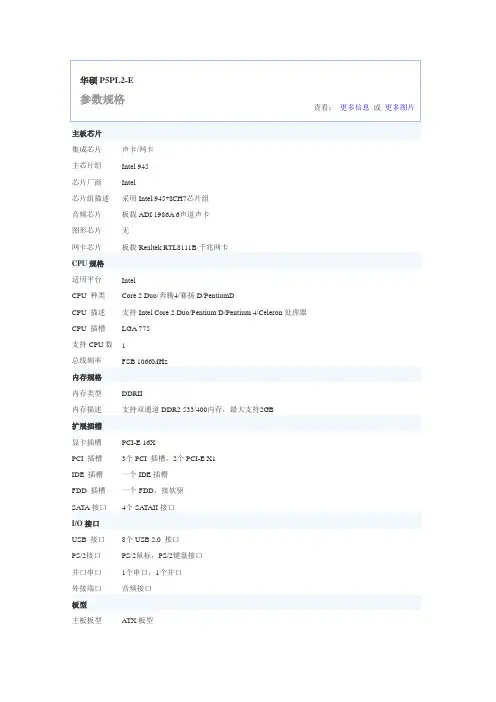
■Operates from Single +5V Power Supply ■Meets All RS-232D and ITU V.28Specifications■Operates with 0.1µF to 10µF Capacitors ■High Data Rate – 120Kbps Under Load ■Low Power Shutdown ≤1µA (Typical)■3-State TTL/CMOS Receiver Outputs ■Low Power CMOS – 3mA Operation ■Improved ESD Specifications:±15kV Human Body Model±15kV IEC1000-4-2 Air Discharge ±8kV IEC1000-4-2 Contact DischargeDESCRIPTION…The SP202E/232E/233E/310E/312E devices are a family of line driver and receiver pairs that meet the specifications of RS-232 and V.28 serial protocols with enhanced ESD performance.The ESD tolerance has been improved on these devices to over ±15KV for both Human Body Model and IEC1000-4-2 Air Discharge Method. These devices are pin-to-pin compatible with Sipex's SP232A/233A/310A/312A devices as well as popular industry standards. As with the initial versions, the SP202E/232E/233E/310E/312E devices feature at least 120Kbps data rate under load, 0.1µF charge pump capacitors, and overall ruggedness for commercial applications.This family also features Sipex's BiCMOS design allowing low power operation without sacrificing performance. The series is available in plastic and ceramic DIP and SOIC packages operating over the commercial, industrial and military temperature ranges.Number of RS232No. of Receivers No. of ExternalModel Drivers Receivers Active in Shutdown 0.1µF CapacitorsShutdown WakeUp TTL Tri–StateSP202E 2204No No No SP232E 2204No No No SP233E 2200No No No SP310E 2204Yes No Yes SP312E2224Yes Yes YesABSOLUTE MAXIMUM RATINGS This is a stress rating only and functional operation of the device at these or any other conditions above those indicated in the operation sections of this specification is not implied. Exposure to absolute maximum rating conditions for extended periods of time may affect reliability.Vcc .................................................................................................................................................................+6VV+....................................................................................................................(Vcc-0.3V) to +11.0V V-............................................................................................................................................................-11.0V Input VoltagesT IN .........................................................................................................................-0.3 to (Vcc +0.3V)RIN ............................................................................................................................................................±15VOutput VoltagesT OUT ....................................................................................................(V+, +0.3V) to (V-, -0.3V)ROUT ................................................................................................................-0.3V to (Vcc +0.3V)Short Circuit DurationT OUT .........................................................................................................................................ContinuousPower DissipationCERDIP..............................................................................675mW(derate 9.5mW/°C above +70°C)Plastic DIP..........................................................................375mW(derate 7mW/°C above +70°C)Small Outline......................................................................375mW(derate 7mW/°C above +70°C)SPECIFICATIONS元器件交易网元器件交易网PERFORMANCE CURVES+Figure 1. Typical Circuit using the SP202E or SP232E.FEATURES…The SP202E/232E/233E/310E/312E devices are a family of line driver and receiver pairs that meet the specifications of RS-232 and V.28serial protocols with enhanced ESD perfor-mance. The ESD tolerance has been improved on these devices to over ±15KV for both Human Body Model and IEC1000-4-2 Air Discharge Method. These devices are pin-to-pin compat-ible with Sipex's 232A/233A/310A/312A devices as well as popular industry standards.As with the initial versions, the SP202E/232E/233E/310E/312E devices feature10V/µs slew rate, 120Kbps data rate under load, 0.1µF charge pump capacitors, overall ruggedness for commercial applications, and increased drive current for longer and more flexible cable configurations. This family also features Sipex's BiCMOS design allowing low power operation without sacrificing performance.The SP202E/232E/233E/310E/312E devices have internal charge pump voltage converters which allow them to operate from a single +5V supply. The charge pumps will operate with polarized or non-polarized capacitors ranging from 0.1 to 10 µF and will generate the ±10V needed to generate the RS-232 output levels.Both meet all EIA RS-232 and ITU V.28specifications.The SP310E provides identical features as the SP232E with a single control line which simultaneously shuts down the internal DC/DC converter and puts all transmitter and receiver outputs into a high impedance state. The SP312E is identical to the SP310E with separate tri-state and shutdown control lines.THEORY OF OPERATIONThe SP232E , SP233E , SP310E and SP312Edevices are made up of three basic circuit blocks –1) a driver/transmitter, 2) a receiver and 3) a charge pump. Each block is described below.Driver/TransmitterThe drivers are inverting transmitters, which ac-cept TTL or CMOS inputs and output the RS-232signals with an inverted sense relative to the input logic levels. Typically the RS-232 output voltage swing is ±9V. Even under worst case loading conditions of 3kOhms and 2500pF, the output is guaranteed to be ±5V, which is consistent with the RS-232 standard specifications. The transmitter outputs are protected against infinite short-circuits to ground without degradation in reliability.元器件交易网The instantaneous slew rate of the transmitteroutput is internally limited to a maximum of 30V/µs in order to meet the standards [EIA RS-232-D 2.1.7, Paragraph (5)]. However, the transition re-gion slew rate of these enhanced products is typi-cally 10V/µs. The smooth transition of the loaded output from V OL to V OH clearly meets the mono-tonicity requirements of the standard [EIA RS-232-D 2.1.7, Paragraphs (1) & (2)].ReceiversThe receivers convert RS-232 input signals to inverted TTL signals. Since the input is usually from a transmission line, where long cable lengthsand system interference can degrade the signal, theinputs have a typical hysteresis margin of 500mV.This ensures that the receiver is virtually immune to noisy transmission lines.The input thresholds are 0.8V minimum and 2.4V maximum, again well within the ±3V RS-232requirements. The receiver inputs are also pro-tected against voltages up to ±15V. Should an input be left unconnected, a 5KOhm pulldown resistor to ground will commit the output of the receiver to a high state.Figure 2. Typical Circuits using the SP233ECP and SP233ECTFigure 3. Typical Circuits using the SP310E and SP312EFigure 4. Charge Pump — Phase 1Figure 5. Charge Pump — Phase 2In actual system applications, it is quite possible for signals to be applied to the receiver inputs before power is applied to the receiver circuitry.This occurs, for example, when a PC user attempts to print, only to realize the printer wasn’t turned on.In this case an RS-232 signal from the PC will appear on the receiver input at the printer. When the printer power is turned on, the receiver will operate normally. All of these enhanced devices are fully protected.Charge PumpThe charge pump is a Sipex –patented design (5,306,954) and uses a unique approach com-pared to older less–efficient designs. The charge pump still requires four external capacitors, but uses a four–phase voltage shifting technique to attain symmetrical 10V power supplies. There is a free–running oscillator that controls the four phases of the voltage shifting. A description of each phase follows.Phase 1— V SS charge storage —During this phase of the clock cycle, the positive side of capacitors C 1 and C 2 are initially charged to +5V. C l + is then switched to ground and the charge in C 1– is transferred to C 2–. Since C 2+ is connected to +5V, the voltage potential across capacitor C 2 is now 10V.Phase 2— V SS transfer — Phase two of the clock con-nects the negative terminal of C 2 to the V SS storage capacitor and the positive terminal of C 2to ground, and transfers the generated –l0V to C 3. Simultaneously, the positive side of capaci-tor C 1 is switched to +5V and the negative side is connected to ground.Phase 3— V DD charge storage — The third phase of the clock is identical to the first phase — the charge transferred in C 1 produces –5V in the negative terminal of C 1, which is applied to the negative side of capacitor C 2. Since C 2+ is at +5V, the voltage potential across C 2 is l0V.Phase 4— V DD transfer — The fourth phase of the clock connects the negative terminal of C 2 to ground,and transfers the generated l0V across C 2 to C 4,the V DD storage capacitor. Again, simultaneously with this, the positive side of capacitor C 1 is switched to +5V and the negative side is con-nected to ground, and the cycle begins again.Since both V + and V – are separately generated from V CC ; in a no–load condition V + and V – willFigure 6. Charge Pump Waveforms+10Va) C 2+GND GNDb) C 2––10VFigure 7. Charge Pump — Phase 3Figure 8. Charge Pump — Phase 4be symmetrical. Older charge pump approachesthat generate V – from V + will show a decrease in the magnitude of V – compared to V + due to the inherent inefficiencies in the design.The clock rate for the charge pump typically operates at 15kHz. The external capacitors can be as low as 0.1µF with a 16V breakdown voltage rating.Shutdown (SD) and Enable (EN) for the SP310E and SP312EBoth the SP310E and SP312E have a shutdown/standby mode to conserve power in battery-pow-ered systems. To activate the shutdown mode,which stops the operation of the charge pump, a logic “0” is applied to the appropriate control line.For the SP310E , this control line is ON/OFF (pin 18). Activating the shutdown mode also puts theSP310E transmitter and receiver outputs in a high impedance condition (tri-stated). The shutdown mode is controlled on the SP312E by a logic “0”on the SHUTDOWN control line (pin 18); this also puts the transmitter outputs in a tri–state mode. The receiver outputs can be tri–stated separately during normal operation or shutdown by a logic “1” on the ENABLE line (pin 1).Wake–Up Feature for the SP312EThe SP312E has a wake–up feature that keeps all the receivers in an enabled state when the device is in the shutdown mode. Table 1 defines the truth table for the wake–up function.With only the receivers activated, the SP312E typically draws less than 5µA supply current. In the case of a modem interfaced to a computer in power down mode, the Ring Indicator (RI) signal from the modem would be used to "wake up" the computer, allowing it to accept data transmission.After the ring indicator signal has propagated through the SP312E receiver, it can be used to trigger the power management circuitry of the computer to power up the microprocessor, and bring the SD pin of the SP312E to a logic high, taking it out of the shutdown mode. The receiver propagation delay is typically 1µs. The enable time for V+ and V– is typically 2ms. After V+ and V– have settled to their final values, a signal can be sent back to the modem on the data terminal ready (DTR) pin signifying that the computer is ready to accept and transmit data.Pin Strapping for the SP233ECTThe SP233E packaged in the 20–pin SOIC pack-age (SP233ECT) has a slightly different pinout than the SP233E in other package configurations. To operate properly, the following pairs of pins must be externally wired together:the two V– pins (pins 10 and 17)the two C2+ pins (pins 12 and 15)the two C2– pins (pins 11 and 16)All other connections, features, functions and performance are identical to the SP233E as specified elsewhere in this data sheet.ESD TOLERANCEThe SP202E/232E/233E/310E/312E devices incorporates ruggedized ESD cells on all driver output and receiver input pins. The ESD struc-ture is improved over our previous family for more rugged applications and environments sen-sitive to electro-static discharges and associated transients. The improved ESD tolerance is at least ±15KV without damage nor latch-up. There are different methods of ESD testing applied:a) MIL-STD-883, Method 3015.7b) IEC1000-4-2 Air-Dischargec) IEC1000-4-2 Direct ContactThe Human Body Model has been the generally accepted ESD testing method for semiconductors. This method is also specified in MIL-STD-883, Method 3015.7 for ESD testing. The premise of this ESD test is to simulate the human body’s potential to store electro-static energy and discharge it to an integrated circuit. The simulation is performed by using a test model as shown in Figure 9. This method will test the IC’s capability to withstand an ESD transient during normal handling such as in manufacturing areas where the ICs tend to be handled frequently.The IEC-1000-4-2, formerly IEC801-2, is generally used for testing ESD on equipment and systems. For system manufacturers, they must guarantee a certain amount of ESD protection since the system itself is exposed to the outside environment and human presence. The premise元器件交易网Table 1. Wake-up Function Truth Table.Figure 9. ESD Test Circuit for Human Body ModelFigure 10. ESD Test Circuit for IEC1000-4-2with IEC1000-4-2 is that the system is required to withstand an amount of static electricity when ESD is applied to points and surfaces of the equipment that are accessible to personnel during normal usage. The transceiver IC receives most of the ESD current when the ESD source is applied to the connector pins. The test circuit for IEC1000-4-2 is shown on Figure 10. There are two methods within IEC1000-4-2, the Air Discharge method and the Contact Discharge method.With the Air Discharge Method, an ESD voltage is applied to the equipment under test (EUT)through air. This simulates an electrically charged person ready to connect a cable onto the rear of the system only to find an unpleasant zap just before the person touches the back panel. The high energy potential on the person discharges through an arcing path to the rear panel of the system before he or she even touches the system.This energy, whether discharged directly or through air, is predominantly a function of theSP202E HUMAN BODY IEC1000-4-2FamilyMODEL Air Discharge Direct Contact LevelDriver Outputs ±15kV ±15kV ±8kV 4Receiver Inputs ±15kV±15kV±8kV4Figure 11. ESD Test Waveform for IEC1000-4-2t=0nst=30ns0A15A30At ➙i ➙Table 2. Transceiver ESD Tolerance Levelsdischarge current rather than the discharge voltage. Variables with an air discharge such as approach speed of the object carrying the ESD potential to the system and humidity will tend to change the discharge current. For example, the rise time of the discharge current varies with the approach speed.The Contact Discharge Method applies the ESD current directly to the EUT. This method was devised to reduce the unpredictability of the ESD arc. The discharge current rise time is constant since the energy is directly transferred without the air-gap arc. In situations such as hand held systems, the ESD charge can be directlydischarged to the equipment from a person already holding the equipment. The current is transferred on to the keypad or the serial port of the equipment directly and then travels through the PCB and finally to the IC.The circuit models in Figures 9 and 10 represent the typical ESD testing circuit used for all three methods. The C S is initially charged with the DC power supply when the first switch (SW1) is on.Now that the capacitor is charged, the second switch (SW2) is on while SW1 switches off. The voltage stored in the capacitor is then applied through R S , the current limiting resistor, onto the device under test (DUT). In ESD tests, the SW2switch is pulsed so that the device under test receives a duration of voltage.For the Human Body Model, the current limiting resistor (R S ) and the source capacitor (C S ) are 1.5k Ω an 100pF, respectively. For IEC-1000-4-2, the current limiting resistor (R S ) and the source capacitor (C S ) are 330Ω an 150pF, respectively.The higher C S value and lower R S value in the IEC1000-4-2 model are more stringent than the Human Body Model. The larger storage capacitor injects a higher voltage to the test point when SW2 is switched on. The lower current limiting resistor increases the current charge onto the test point.元器件交易网ORDERING INFORMATIONModel.......................................................................................Temperature Range................................................................................Package SP202ECN.....................................................................................0°C to +70°C...........................................................................16–pin N–SOIC SP202ECP.....................................................................................0°C to +70°C.......................................................................16–pin Plastic DIP SP202ECT.....................................................................................0°C to +70°C................................................................................16–pin SOIC SP202EEN...................................................................................–40°C to +85°C..........................................................................16–pin N-SOIC SP202EEP...................................................................................–40°C to +85°C.....................................................................16–pin Plastic DIP SP202EET...................................................................................–40°C to +85°C..............................................................................16–pin SOICSP232ECN.....................................................................................0°C to +70°C...........................................................................16–pin N–SOIC SP232ECP.....................................................................................0°C to +70°C.......................................................................16–pin Plastic DIP SP232ECT.....................................................................................0°C to +70°C................................................................................16–pin SOIC SP232EEN...................................................................................–40°C to +85°C..........................................................................16–pin N-SOIC SP232EEP...................................................................................–40°C to +85°C.....................................................................16–pin Plastic DIP SP232EET...................................................................................–40°C to +85°C..............................................................................16–pin SOIC SP233ECP.....................................................................................0°C to +70°C.......................................................................20–pin Plastic DIP SP233ECT.....................................................................................0°C to +70°C................................................................................20–pin SOIC SP233EEP...................................................................................–40°C to +85°C.....................................................................20–pin Plastic DIP SP233EET...................................................................................–40°C to +85°C..............................................................................20–pin SOICSP310ECP.....................................................................................0°C to +70°C.......................................................................18–pin Plastic DIP SP310ECT.....................................................................................0°C to +70°C................................................................................18–pin SOIC SP310ECA.....................................................................................0°C to +70°C...............................................................................20–pin SSOP SP310EEP...................................................................................–40°C to +85°C.....................................................................18–pin Plastic DIP SP310EET...................................................................................–40°C to +85°C..............................................................................18–pin SOIC SP310EEA...................................................................................–40°C to +85°C.............................................................................20–pin SSOP SP312ECP.....................................................................................0°C to +70°C.......................................................................18–pin Plastic DIP SP312ECT.....................................................................................0°C to +70°C................................................................................18–pin SOIC SP312ECA.....................................................................................0°C to +70°C...............................................................................20–pin SSOP SP312EEP...................................................................................–40°C to +85°C.....................................................................18–pin Plastic DIP SP312EET...................................................................................–40°C to +85°C..............................................................................18–pin SOIC SP312EEA...................................................................................–40°C to +85°C.............................................................................20–pin SSOPPlease consult the factory for pricing and availability on a Tape-On-Reel option.CorporationSIGNAL PROCESSING EXCELLENCESipex CorporationHeadquarters andSales Office22 Linnell CircleBillerica, MA 01821TEL: (978) 667-8700FAX: (978) 670-9001e-mail: sales@Sales Office233 South Hillview DriveMilpitas, CA 95035TEL: (408) 934-7500FAX: (408) 935-7600Sipex Corporation reserves the right to make changes to any products described herein. Sipex does not assume any liability arising out of the application or use of any product or circuit described hereing; neither does it convey any license under its patent rights nor the rights of others.。