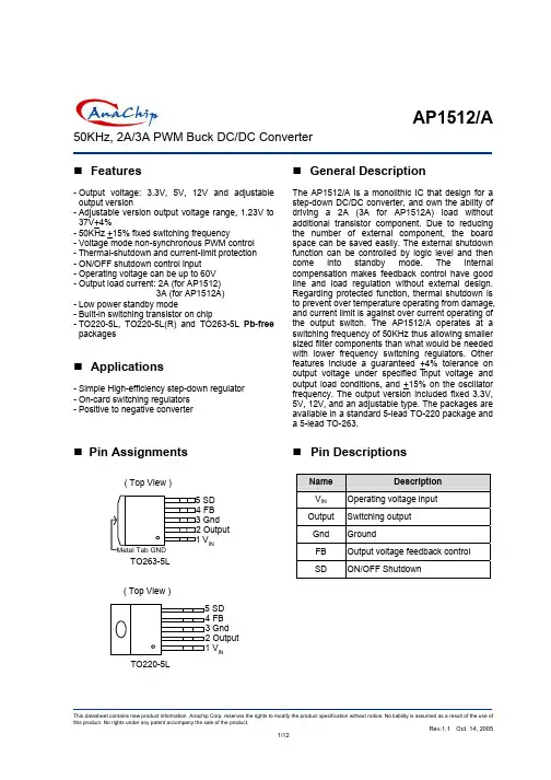
AP1512/A50KHz, 2A/3A PWM Buck DC/DC ConverterFeatures- Output voltage: 3.3V, 5V, 12V and adjustable output version- Adjustable version output voltage range, 1.23V to 37V+4%- 50KHz +15% fixed switching frequency- Voltage mode non-synchronous PWM control - Thermal-shutdown and current-limit protection - ON/OFF shutdown control input - Operating voltage can be up to 60V - Output load current: 2A (for AP1512)3A (for AP1512A)- Low power standby mode- Built-in switching transistor on chip - TO220-5L, TO220-5L(R) and TO263-5L Pb-free packagesApplications- Simple High-efficiency step-down regulator - On-card switching regulators - Positive to negative converterGeneral DescriptionThe AP1512/A is a monolithic IC that design for a step-down DC/DC converter, and own the ability of driving a 2A (3A for AP1512A) load without additional transistor component. Due to reducing the number of external component, the board space can be saved easily. The external shutdown function can be controlled by logic level and then come into standby mode. The internal compensation makes feedback control have good line and load regulation without external design. Regarding protected function, thermal shutdown is to prevent over temperature operating from damage, and current limit is against over current operating of the output switch. The AP1512/A operates at a switching frequency of 50KHz thus allowing smaller sized filter components than what would be needed with lower frequency switching regulators. Other features include a guaranteed +4% tolerance on output voltage under specified input voltage and output load conditions, and +15% on the oscillator frequency. The output version included fixed 3.3V, 5V, 12V, and an adjustable type. The packages are available in a standard 5-lead TO-220 package and a 5-lead TO-263.Pin AssignmentsTO220-5L( Top View )( Top View )TO263-5L INMetal Tab GNDINPin DescriptionsNameDescriptionV IN Operating voltage input Output Switching output Gnd Ground FBOutput voltage feedback controlSD ON/OFF ShutdownAP1512/A50KHz, 2A/3A PWM Buck DC/DC ConverterOrdering InformationPackage T5: TO220-5LK5: TO263-5LOutput Version AP1512 X XX X XPacking Blank : Tube A : TapingBlank : Adjustable -33 : 3.3V -50 : 5.0V -12 : 12VT5R: TO220-5L(R)Part Number Blank: 2A A : 3ABlock DiagramCurrent Source bias1.235V Reference2.5V Regulator50KHz OSC.Start up++_+_Thermal LimitPre-driverComp CompGndOutput V INSDFB220mV200mV2A Switch +__Amp CompFrequecy compen-sation(3A for AP1512A)AP1512/A50KHz, 2A/3A PWM Buck DC/DC ConverterAbsolute Maximum RatingsSymbol Parameter RatingUnit V CC Supply Voltage +63 V V SD ON/OFF Pin input voltage -0.3 to +40 V V FB Feedback Pin voltage -0.3 to +40V V OUT Output voltage to Ground -1V P D Power dissipation Internally limited W T ST Storage temperature -65 to +150 o C T OP Operating temperature -40 to +125 o C V OP Operating voltage+4.5 to +60VElectrical Characteristics (All Output Voltage Versions)Unless otherwise specified, V IN =30V for all version. I LOAD = 0.5ASymbol ParameterConditionsMin.Typ.Max. Unit 8I BFeedback bias currentV FB =1.3V(Adjustable version only)5 10µA42.5 50 57.5F OSC oscillator frequency40 60KHz1.4V SAT saturation voltage I OUT =2A no outside circuitV FB =0V force driver on1.3 1.5VMax. Duty Cycle(ON) V FB =0V force driver on100DCMin. Duty cycle(OFF) V FB =12V force driver off%4.5I CL current limit for AP1512 peak currentno outside circuitV FB =0V force driver on 2.5 3 5.5A5I CL current limit for AP1512A peak current no outside circuitV FB =0V force driver on3.2 4 6 A Output = 0no outside circuitV FB =12V force driver off-250 uA I L Output = -1 Output leakage currentV IN =60V -2 -60 mA I Q Quiescent Current V FB =12V force driver off 5 10 mA450 I STBYStandby Quiescent Current ON/OFF pin=5VV IN =60V 350 500uA V IL Low (regulator ON) - 0.6 V IH ON/OFF pin logic inputthreshold voltage High (regulator OFF) 2.0 1.3 - VI H ON/OFF pin logic input currentV LOGIC =2.5V (OFF) 0 -5I L ON/OFF pin input current V LOGIC =0.5V (ON) -0.8 -10uA TO220-5L 2.5 θJC Thermal Resistance TO263-5L Junction to case3.5 oC/WTO220-5L 28 θJA Thermal ResistanceWith copper area ofapproximately 3 in 2TO263-5L Junction to ambient 23 oC/WAP1512/A50KHz, 2A/3A PWM Buck DC/DC ConverterElectrical Characteristics (Continued)AP1512Symbol Parameter Conditions Typ. Limit Unit AP1512-ADJ FB V Output Feedback 10V < V IN < 60V 0.2A < I LOAD < 2AV OUT programmed for 3V 1.231.193/1.18 1.267/1.28 V V MIN V MAX AP1512-3.3V OUT V Output voltage 10V < V IN < 60V 0.2A < I LOAD < 2A 3.3 3.168/3.135 3.432/3.465 V V MIN V MAX AP1512-5VOUT V Output voltage 10V < V IN < 60V 0.2A < I LOAD < 2A 5 4.8/4.75 5.2/5.25 V V MIN V MAX OUT V Output voltage15V < V IN < 60V 0.2A < I LOAD < 2A12 11.52/11.4 12.48/12.6V V MIN V MAX AP1512-12VηEfficiency V IN = 30V, I LOAD = 2A 83 % AP1512ASymbol Parameter Conditions Typ. Limit Unit AP1512A-ADJ FB V Output Feedback 10V < V IN < 60V 0.2A < I LOADV OUT programmed for 3V 1.231.193/1.18 1.267/1.28 V V MIN V MAX AP1512A-3.3V OUT V Output voltage 10V < V IN < 60V 0.2A < I LOAD 3.3 3.168/3.135 3.432/3.465 V V MIN V MAX AP1512A-5VOUT VOutput voltage10V < V IN < 60V 0.2A < I LOAD54.8/4.755.2/5.25V V MIN V MAX OUT V Output voltage15V < V IN < 60V 0.2A < I LOAD12 11.52/11.4 12.48/12.6V V MIN V MAX AP1512A-12VηEfficiency V IN = 30V, I LOAD = 3A80%Specifications with boldface type are for full operating temperature range, the other type are for T J =25ºC.Typical Performance CharacteristicsAP1512A Current Limit v.s. Temperature(Vcc=60V, Vout=5V)33.23.43.63.84-50050100150Temperature (TA) (°C)C u r r e n t L i m i t (A )AP1512A Efficiency v.s. Supply Voltage(Vout=5V, Iout=3A)10203040506070809010001224364860Supply Voltage(V)E f f i c i e n c y (%)AP1512/A50KHz, 2A/3A PWM Buck DC/DC ConverterTypical Performance Characteristics (Continued)AP1512 Efficiency v.s. Temperature(Vin=12V,Vout=5V,Io=2A)102030405060708090100-50-30-101030507090*********Temperature (TA) (°C)E f f i c i e n c y (%)AP1512 Efficiency v.s. Temperature(Vin=12V,Vout=3.3V,Io=2A)102030405060708090100-50-30-101030507090*********Temperature (TA) (°C)E f f i c i e n c y (%)AP1512 Supply Current v.s. Temperature(Vcc=12V , No Load ,Von/off =0V(Switch ON) ,Von/off =5V(Switch OFF))12345678-40-25-105203550658095110125S u p p l y C u r r e n t (m A )Temperature (TA) (°C)Switch ON102030405060708090100-40-25-105203550658095110125S u p p l y C u r r e n t (u A )Temperature (TA) (°C)Switch OFFAP1512 Output Voltage v.s. Temperature(Vin=12V, Vout=5V, Io=1A)4.704.754.804.854.904.955.005.055.10-50050100150O u t p u t V o l t a g e (V )Temperature (TA) (°C)AP1512 Threshold Voltage v.s. Temperature(Vcc=12V, Vout=5V)00.20.40.60.811.21.41.6-50050100150T h r e s h o l d V o l t a g e (V )Temperature (TA) (°C)AP1512/A50KHz, 2A/3A PWM Buck DC/DC ConverterTypical Performance Characteristics (Continued)AP1512 Frequency v.s. Temperature(Vcc=12V, Io=1A, Vout=5V)4045505560-50-30-101030507090110130150Temperature (TA) (°C)F r e q u e n c y (K H z )AP1512 Current Limit v.s. Temperature(Vcc=60V, Vout=5V)2.833.23.43.6-5050100150C u r r e n t L i m i t (A )Temperature (TA) (°AP1512 Quiescent Current v.s. Supply Voltage(force driver off)5.25.45.65.866.21224364860Q u i e s c e n t C u r r e n t (A )Supply Voltage(V)AP1512/A50KHz, 2A/3A PWM Buck DC/DC ConverterTypical Application Circuit(1) Adjustable Type CircuitA. Vin=10V~60V, Vout=5V; Iout=0.3A~2A, Iout below 0.3A DCMC51nL147uH12R23KVinC21uD1SR360ON/OFFR31KC1100uF/100VAP1512/A15243VinSDOUTPUTFBGND 0.1uC3470uF/16VC7B. Vin=10V~60V, Vout=3.3V, Iout=0.3A~2A, Iout below 0.3A DCMC51nL147uH12R22KVinC21uD1SR360ON/OFFR31.2KC1100uF/100VAP1512/A15243VinSDOUTPUTFBGND 0.1uC3470uF/16VC7(2) Fixed Type CircuitA. Vin=10V~60V, Vout=5V, Iout=0.7A~2A, Iout below 0.7A DCML147uH12VinC21uD1SR360ON/OFFC1100uF/100VVoutAP1512/A15243VinSDOUTPUTFBGND 10nC3470uF/16VC7AP1512/A50KHz, 2A/3A PWM Buck DC/DC ConverterTypical Application Circuit (Continued)B. Vin=10V~60V, Vout=3.3V, Iout=0.7A~2A, Iout below 0.7A DCML133uH12VinC23.3uD1SR360ON/OFFC1220uF/100VVoutAP1512/A15243VinSDOUTPUTFBGND 3.3uC31500uF/16VC7Function Description+V INThis is the positive input supply for the IC switching regulator. A suitable input bypass capacitor must be present at this pin to minimize voltage transients and to supply the switching currents needed by the regulator.GroundCircuit ground.OutputInternal switch. The voltage at this pin switches between (+V IN – V SAT ) and approximately – 0.5V, with a duty cycle of approximately V OUT / V IN . To minimize coupling to sensitive circuitry, the PC board copper area connected to this pin should be kept a minimum.FeedbackSenses the regulated output voltage to complete the feedback loop.ON /OFFAllows the switching regulator circuit to be shutdown using logic level signals thus dropping the total input supply current to approximately 150uA. Pulling this pin below a threshold voltage of approximately 1.3V turns the regulator on, and pulling this pin above 1.3V (up to a maximum of 40V) shuts the regulator down. If this shutdown feature is not needed, the SD pin can be wired to the ground pin or it can be left open, in either case the regulator will be in the ON condition.Thermal ConsiderationsThe AP1512/A is available in two packages, a 5-pin TO-220 and a 5-pin surface mount TO-263.The TO-220 package needs a heat sink under most conditions. The size of the heatsink depends on the input voltage, the output voltage, the load current and the ambient temperature. The AP1512/A junction temperature rises above ambient temperature for a 2A load and different input and output voltages. The data for these curves was taken with the AP1512/A (TO-220 package) operating as a buckswitching regulator in an ambient temperature of 25o C (still air). These temperature rise numbers are all approximate and there are many factors that can affect these temperatures. Higher ambient temperatures require more heat sinking.The TO-263 surface mount package tab is designed to be soldered to the copper on a printed circuit board. The copper and the board are the heat sink for this package and the other heat producing components, such as the catch diode and inductor. The PC board copper area that the package is soldered to should be at least 0.4 in 2, and ideally should have 2 or more square inches of 2 oz. Additional copper area improves the thermal characteristics, but with copper areas greater than approximately 6 in 2, only small improvements in heat dissipation are realized. If further thermal improvements are needed, double sided, multilayer PC board with large copper areas and/or airflow are recommended.AP1512/A50KHz, 2A/3A PWM Buck DC/DC ConverterFunction Description (Continued)The AP1512/A (TO-263 package) junction temperature rise above ambient temperature with a 2A load for various input and output voltages. This data was taken with the circuit operating as a buck switching regulator with all components mounted on a PC board to simulate the junction temperature under actual operating conditions. This curve can be used for a quick check for the approximate junction temperature for various conditions, but be aware that there are many factors that can affect the junction temperature. When load currents higher than 2A are used, double sided or multilayer PC boards with large copper areas and/or airflow might be needed, especially for high ambient temperatures and high output voltages.For the best thermal performance, wide copper traces and generous amounts of printed circuit board copper should be used in the board layout. (Once exception to this is the output (switch) pin, which should not have large areas of copper.) Large areas of copper provide the best transfer of heat (lower thermal resistance) to the surrounding air, and moving air lowers the thermal resistance even further.Package thermal resistance and junction temperature rise numbers are all approximate, and there are many factors that will affect these numbers. Some of these factors include board size, shape, thickness, position, location, and even board temperature. Other factors are, trace width, total printed circuit copper area, copper thickness, single or double-sided, multilayer board and the amount of solder on the board. The effectiveness of the PC board to dissipate heat also depends on the size, quantity and spacing of other components on the board, as well as whether the surrounding air is still or moving. Furthermore, some of these components such as the catch diode will add heat to the PC board and the heat can vary as the input voltage changes. For the inductor, depending on the physical size, type of core material and the DC resistance, it could either act as a heat sink taking heat away from the board, or it could add heat to the board.Marking Information(1) TO263-5L1512X-XX Blank: ADJ ( Top View )"02" = 2002"01" = 2001YY WW X01~52~Part Number:A: AP1512A(2) TO220-5L1512X-XX ID codeYear:"02" = 2002"01" = 2001YY WW XXth week:01~52~Blank: ADJ LogoPart Number:-Output Type: -33: 3.3V -50: 5.0V -12: 1.2V Blank: AP1512A: AP1512AAP1512/A 50KHz, 2A/3A PWM Buck DC/DC ConverterPackage Information(1) Package Type: TO220-5LD QEbe1AJ1FCΦPH1LeDimensions In Millimeters Dimensions In InchesSymbolMin. Nom. Max. Min. Nom. Max.A 4.07 4.45 4.82 0.160 0.175 0.190b 0.76 0.89 1.02 0.030 0.035 0.040C 0.36 0.50 0.64 0.014 0.020 0.025D 14.22 14.86 15.50 0.560 0.585 0.610E 9.78 10.16 10.54 0.385 0.400 0.415e 1.57 1.71 1.85 0.062 0.067 0.073e1 6.68 6.81 6.93 0.263 0.268 0.273F 1.14 1.27 1.40 0.045 0.050 0.055H1 5.46 6.16 6.86 0.215 0.243 0.270 J1 2.29 2.74 3.18 0.090 0.108 0.125 L 13.21 13.97 14.73 0.520 0.550 0.580 Øp 3.68 3.81 3.94 0.145 0.150 0.155 Q 2.54 2.73 2.92 0.100 0.107 0.115AP1512/A 50KHz, 2A/3A PWM Buck DC/DC ConverterPackage Information (Continued)(2) Package Type: TO263-5LEL2e B DLAC2CL11.02.515.710.99.11.7Land Pattern Recommendation (Unit: mm)Dimensions In Millimeters Dimensions In InchesSymbolMin. Nom. Max. Min. Nom. Max.A 4.07 4.46 4.85 0.160 0.176 0.191B 0.66 0.84 1.02 0.026 0.033 0.040C 0.36 0.50 0.64 0.014 0.020 0.025C2 1.14 1.27 1.40 0.045 0.050 0.055D 8.65 9.15 9.65 0.341 0.360 0.380E 9.78 10.16 10.54 0.385 0.400 0.415e 1.57 1.71 1.85 0.062 0.068 0.073L 14.61 15.24 15.88 0.575 0.600 0.625 L1 2.29 2.54 2.79 0.090 0.100 0.110 L2 - - 2.92 - - 0.115AP1512/A50KHz, 2A/3A PWM Buck DC/DC ConverterPackage Information (Continued)(3) Package Type: TO220-5L(R) Mechanical drawingEQDbAFH1d1d2J3J1J2eH2H3AJ1J2J3EDimensions In Millimeters Dimensions In Inches SymbolMin. Nom. Max. Min. Nom. Max.A 4.4 4.6 4.7 0.175 0.180 0.185b 0.7 0.8 0.9 0.027 0.032 0.037 D 8.4 8.7 8.9 0.330 0.340 0.350 d1 1.0 0.039 d2 6.3 0.248 E 9.91 10.16 10.41 0.390 0.400 0.410 e 1.6 1.7 1.8 0.062 0.067 0.072 F 1.2 1.25 1.3 0.048 0.050 0.052 H1 6.4 0.250 H2 20.8 21.6 22.4 0.820 0.850 0.880 H3 23.9 24.7 25.5 0.942 0.972 1.002 J1 2.7 0.105 J2 3.7 4.5 5.3 0.147 0.177 0.207 J3 8.4 0.331 Q 2.5 2.8 3.0 0.100 0.110 0.120。