SD6832说明书_1.2-L
- 格式:pdf
- 大小:338.28 KB
- 文档页数:9

产品规格分类内置高压MOSFET 电流模式PWM+PFM 控制器系列描述SD6832是用于开关电源的内置高压MOSFET 外置采样电阻的电流模式PWM+PFM 控制器系列产品。
该电路待机功耗低,启动电流低。
在待机模式下,电路进入打嗝模式,从而有效地降低电路的待机功耗。
电路的开关中心频率为25~67KHz ,随负载而定。
抖动的开关频率,可以获得较低的EMI 。
内置峰值电流补偿电路,可以使不同交流电压输入时极限峰值电流一致。
上电时,峰值电流补偿最大,然后逐渐达到平衡,可以减小在上电过程中变压器的应力,防止变压器饱和。
还可以通过CS 端电阻调节极限峰值电流。
电路内部集成了各种异常状态保护功能。
包括欠压锁定,过压保护,过载保护,脉冲前沿消隐,原线圈过流保护和温度保护功能。
在电路发生保护以后,电路可以不断自动重启,直到系统正常为止。
主要特点∗ 能源之星2.0标准 ∗ 低启动电流(3µA )∗ 随负载而变的开关频率可以提高效率 ∗ 抖动的开关频率可以降低EMI ∗ 过压、原线圈过流、过载、过温保护 ∗ 外置峰值电流采样电阻 ∗ 欠压锁定∗ 内部集成高压MOSFET ∗ 自动重启 ∗ 峰值电流补偿电路∗ 初始化峰值电流最大补偿,实现软启动功能 ∗ 打嗝模式 ∗逐周期限流应用∗ 开关电源典型输出功率能力内部框图注:1. 脉冲宽度由最大结温决定;2. L=51mH, T J=25°C(起始)。
电气参数(感应MOSFET部分,除非特殊说明, T=25°C)amb式PWM+PFM控制器。
控制器包含有振荡频率发生器及各个保护功能。
振荡电路产生的频率抖动,可以降低EMI。
最大峰值电流补偿减小了电路启动时变压器的应力。
通过CS端电阻可以调节极限峰值电流。
在轻载时,电路采用打嗝模式,可以有效的降低电路的待机功耗。
保护功能包括:欠压锁定,过压保护,过载保护,原线圈过流保护和温度保护功能。
电路的前沿消隐功能,保证MOSFET的开通有最短的时间,消除了由于干扰引起的MOSFET的误关断。

IO-Link Interface DescriptionSD6800I O D D -P D F C r e a t o r V 2.0.0.122i f m -000516-20200429-I O D D 1.1, V 1.3.60.970585C o p y r i g h t 2020, B u i l d e r : 4.4.7.7, T i m e : 09:04:15内容1 设备类型 (4)2 通信 (5)3 参数摘要 (6)4 System Commands (10)5 Identification (11)6 Observation (12)6.1 处理数据输入/输出 (12)7 Parameter (14)7.1 输出配置 (14)7.2 数字输出 1 (14)7.3 脉冲输出 1 (15)7.4 数字输出 2 (16)7.5 脉冲输出 2 (17)7.6 模拟输出 2 (17)7.7 数字输入 2 (18)7.8 内存 (18)7.9 故障配置输出 1 (19)7.10 故障配置输出 2 (19)7.11 累加器 (20)7.12 应用配置 (20)7.13 减弱 (21)7.14 传感器显示器的设置 (21)7.15 彩色框架流量 (23)7.16 彩色框架温度 (23)7.17 彩色框架压力 (24)7.18 模拟 (24)7.19 设置 (25)8 Diagnosis (27)8.1 诊断 (27)9 事件 (30)10 错误类型 (31)内容11 单位换算 (32)1 设备类型SD6800压缩空气流量计, 0.10...10.00 m³/h,R 1/2"2 通信供应商ID310 / Bytes 1-54 (hex: 01-36)设备ID1302 / Bytes 0-5-22 (hex: 00-05-16)比特率COM2最短循环时间7,2 msSIO模式支持是块参数是数据存储是Supported profiles Identification and DiagnosisMeasurement Data Channel (standardresolution)Support of IO-Link 1.0是NOTE:If the Vendor ID and Device ID is referenced in your PLC system, then it is ensured that- the connected Device type is correct- the IO-Link datastorage is enabled- your application is still able to work, even your Device has been exchanged with a successor model.For process value update rate, as well as further information concerning sensor performance, seedatasheet3 参数摘要3 参数摘要3 参数摘要4 System CommandsSystem Command information- Address: Index 2, Subindex 0- Datatype: UInteger (8 Bit)- AccessRight: Write Only4 System Commands5 Identification6 Observation6.1 处理数据输入/输出累加器Float32T自上次复位不断累加体积流量的数量计值范围 [m³](0 To 10000000) * 1流量IntegerT (16 Bit)当前流量值范围 [m³/h](0 To 12000) * 0.00132760(OL)32762(cr.OL)32764(NoData)温度IntegerT (16 Bit)当前温度值范围 [°C](-2400 To 7400) * 0.01-32760(UL)32760(OL)-32762(cr.UL)32762(cr.OL)32764(NoData)压力IntegerT (16 Bit)当前压力值范围 [bar](-100 To 2000) * 0.01-32760(UL)32760(OL)32764(NoData)设备状态UIntegerT (4 Bit)当前设备状态,[设备状态 指数 36] 变量的副本在过程数据通道中值范围0(设备正常)1(需要维护)2(不合规格)3(功能性检查)4(失败)数字输入 [OUT2]BooleanT当前的数字信号状态[OUT2]值范围false(OFF)true(On)数字输入 [OUT1]BooleanT当前的数字信号状态[OUT1]值范围false(OFF)true(On)6 ObservationProcess data displayed according device sort order.Please note: Siemens PLCs swap the high and low byte when using byte addressing.过程数据输出RecordT (8 Bit) TotaliserInactive BooleanT设置数字信号 [TotaliserInactive]值范围false(OFF)true(On)7 Parameter7.1 输出配置7.2 数字输出 17 Parameter7.2.1 流量7.2.2 压力7.2.3 温度7.3 脉冲输出 17.3.1 脉冲输出 17 Parameter7.4 数字输出 27.4.1 流量7.4.2 压力7.4.3 温度7 Parameter7.5 脉冲输出 27.5.1 脉冲输出 27.6 模拟输出 27.6.1 流量7.6.2 压力7 Parameter7.6.3 温度7.7 数字输入 27.8 内存7.8.1 流量7.8.2 压力7 Parameter7.8.3 温度7.9 故障配置输出 17.10 故障配置输出 27 Parameter7.11 累加器7.12 应用配置7 Parameter7.13 减弱7.14 传感器显示器的设置7 Parameter7 Parameter7.15 彩色框架流量7.15.1 彩色框架流量7.16 彩色框架温度7.16.1 彩色框架温度7 Parameter7.17 彩色框架压力7.17.1 彩色框架压力7.18 模拟7.18.1 流量7.18.2 压力7 Parameter7.18.3 温度7.19 设置7.19.1 流量7.19.2 压力7 Parameter7.19.3 温度8 Diagnosis8.1 诊断8 Diagnosis8 Diagnosis9 事件Events are raised by the device itself to notify irregular device statesPQ* = Process data quality10 错误类型Error types are used for the ISDU response. Values unequal '0' indicate the cause of a failed ISDU reador write service.11 单位换算This list provides conversion formulas to convert the transmitted IO-Link raw data into physical units.累加器值 [m³]=提供价值*1值 [ft³]=提供价值*35.3146667流量值 [m³/h]=提供价值*0.001值 [ft/s]=提供价值*0.00436352值 [ft³/min]=提供价值*0.00058857值 [ft³/h]=提供价值*0.03531466值 [m/s]=提供价值*0.00133值 [l/min]=提供价值*0.01666666压力值 [bar]=提供价值*0.01值 [psi]=提供价值*0.1450377值 [kPa]=提供价值*1温度值 [°C]=提供价值*0.01值 [°F]=提供价值*0.018 + 32。

TC6832ES.(文件编号:S&CIC1440)非隔离降压型LED恒流控制器概述TC6832ES.是一款高精度降压型LED恒流驱动芯片。
芯片工作在电感电流临界连续模式。
TC6832ES.芯片内部集成500V功率开关,采用专利的驱动和电流检测方式,芯片的工作电流极低,无需辅助绕组检测和供电,只需要很少的外围元件,即可实现优异的恒流特性,极大的节约了系统成本和体积。
TC6832ES.芯片内带有高精度的电流采样电路,同时采用了专利的恒流控制技术,实现高精度的LED恒流输出和优异的线电压调整率。
芯片工作在电感电流临界模式,输出电流不随电感量和LED工作电压的变化而变化,实现优异的负载调整率。
TC6832ES.具有多重保护功能,包括LED开路/短路保护,欠压保护,芯片温度过热调节等。
特点电感电流临界连续模式内部集成500V功率管无需辅助绕组检测和供电芯片超低工作电流宽输入电压±5%LED输出电流精度LED开路保护LED短路保护芯片供电欠压保护过热调节功能封装形式:SOP-8应用LED蜡烛灯、LED球泡灯其它LED照明TC6832ES.(文件编号:典型应用电路2D1-D4TC6832ES.(文件编号:S&CIC1440)非隔离降压型LED恒流控制器极限参数并不完全保证满足个别性能指标。
电气参数定义了器件在工作范围内并且在保证特定性能指标的测试条件下的直流和交流电参数规范。
对于未给定上下限值的参数,该规范不予保证其精度,但其典型值合理反映了器件性能。
注2:温度升高最大功耗一定会减小,这也是由T JMAX,θJA,和环境温度T A所决定的。
最大允许功耗为P DMAX=(T JMAX-T A)/θJA或是极限范围给出的数字中比较低的那个值。
注3:人体模型,100pF电容通过1.5KΩ电阻放电。
推荐工作范围TC6832ES.(文件编号:S&CIC1440)非隔离降压型LED恒流控制器电气参数(无特别说明情况下,V CC=15V,T A=25℃)注5:规格书的最小、最大规范范围由测试保证,典型值由设计、测试或统计分析保证。


SD8-32 CPS控制与保护开关使用说明书一.用途SD8-32 CPS控制与保护开关,以下简称“产品”,适用于交流380V、频率50Hz 的电路中, 用于就近或远距离,手动或自动控制电动机(设备电源)的起动运行和停止,同时用作电动机(设备电源)的缺相、过载、漏电、过、欠电压保护。
产品集成化程度高,单壳体内具备“接触器”+“电动机保护器”+“漏电保护器”的全部功能;傻瓜化设计,专业和非熟练人员均能自如使用,模数化轨道安装,也可螺钉安装;操作简便,状态指示明确,安装、接线极为方便,特别是能有效地防止电动机在自动控制状态下,因缺相起动、运行而烧毁。
二.型号命名及含义:单相或三相表示(三相不标)控制与保护开关壳架额定电流设计序号三明市低压电器厂缩写三. 使用场所的环境要求:3.1安装地点的海拔高度不超过2000m3.2周围空气温度不超过+40℃,下限不低于-5℃,24小时平均值不超过35℃。
3.3.大气的相对湿度,在周围最高温度为40℃时, 不超过50%,在最湿月的月平均温度25℃,月平均最大相对湿度为90%,并考虑到因温度变化发生在产品表面上的凝露。
3.4无雨雪侵袭和显著振动的地方。
3.5污染等级按GB/T14048.1污染等级3级。
3.6安装类别为安装类别Ⅲ。
四. 基本技术参数与特性:4.1额定电压单相AC220V,三相AC380V4.2额定频率50Hz4.3壳架额定电流32A4.4额定电流2.5A(1-4A)、6A(4-8A)、10A(8-15A)、20A(15-25A)、32A(25-35A)。
4.5 机械寿命1000万次,其中电寿命100万次。
4.6 使用类别使用类别为AC-3和AC-1。
4.7过、欠电压保护特性:起动器在电源电压为额定电压Ue的85%~115%范围内能可靠地吸合,超过该规定值,并在规定的时间内不能恢复时即脱扣保护。
4.8过电流动作特性:五. 外形及安装尺寸:六.保护功能:1.在三相电流从电网至电动机的任意一相小于设定电流的50%时,起动器能防止电动机起动和运转;2.过载保护按4.8条的规定;3.漏电保护出厂设定为100m A±10%,用户如有要求可在订贷时说明;4.过、欠压保护出厂设定为85-115%Ue, 用户如有要求可在订贷时说明。


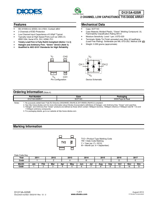
2 CHANNEL LOW CAPACITANCE TVS DIODE ARRAYFeatures• IEC 61000-4-2 (ESD): Air ±15kV, Contact ±8kV • 2 Channels of ESD Protection• Low Channel Input Capacitance of 0.85pF Typical • Typically Used at High Speed Ports such as USB 2.0, IEEE1394, Serial ATA, DVI, HDMI, PCI• Totally Lead-Free & Fully RoHS Compliant (Notes 1 & 2) • Halogen and Antimony Free. “Green” Device (Note 3) • Qualified to AEC-Q101 Standards for High ReliabilityMechanical Data• Case: SOT143 • Case Material: Molded Plastic, “Green” Molding Compound. ULFlammability Classification Rating 94V-0 • Moisture Sensitivity: Level 1 per J-STD-020 • Terminals: Matte Tin Finish annealed over Alloy 42 leadframe(Lead Free Plating). Solderable per MIL-STD-202, Method 208 • Weight: 0.009 grams (approximate)Ordering Information (Note 4)Part NumberCase Packaging D1213A-02SR-7SOT143 3000/Tape & ReelNotes: 1. No purposely added lead. Fully EU Directive 2002/95/EC (RoHS) & 2011/65/EU (RoHS 2) compliant.2. See for more information about Diodes Incorporated’s definitions of Halogen- and Antimony-free, "Green" and Lead-free.3. Halogen- and Antimony-free "Green” products are defined as those which contain <900ppm bromine, <900ppm chlorine (<1500ppm total Br + Cl) and <1000ppm antimony compounds.4. For packaging details, go to our website at .Marking InformationDate Code KeyYear 2011 2012 2013 2014 2015 2016 2017 Code Y Z A B C D EMonth Jan Feb Mar AprMay Jun Jul Aug Sep Oct Nov DecCode 1 2 3 4 5 6 7 8 9 O NDPin ConfigurationDevice SchematicTV2 = Product Type Marking Code YM = Date Code Marking Y = Year (ex: Z = 2012) M = Month (ex: 9 = September) V V NCH2CH1Maximum Ratings (@T A = +25°C, unless otherwise specified.)Characteristic Symbol Value Unit ConditionsOperating Supply Voltage V P - V N6.0 V — DC Voltage at any Channel Input — (V N – 0.5) to (V P + 0.5)V — Peak Pulse Current I PP 5 A 8/20µs, Per Figure 2 ESD Protection – Contact Discharge V ESD_Contact ±8 kV Standard IEC 61000-4-2 ESD Protection – Air Discharge V ESD_Air±15 kV Standard IEC 61000-4-2Thermal CharacteristicsCharacteristic Symbol Value Unit Power Dissipation (Note 5) P D400 mW Thermal Resistance, Junction to Ambient (Note 5) R θJA310 °C/W Operating and Storage Temperature Range T J , T STG -65 to +150 °CElectrical Characteristics (@T A = +25°C, unless otherwise specified.)CharacteristicSymbol Min Typ Max Unit Test ConditionsOperating Supply VoltageV P —3.3 5.5 V — Operating Supply Current (Note 6) I P — — 8.0 µA (V P – VN ) = 3.3V Channel Leakage Current (Note 6) I R — ±0.1 ±1.0 µA V P = 5V, V N = 0V Reverse breakdown voltageV BR 6.0 — — V I R = 1mAClamping Voltage, Positive TransientsV CL1 — 10.0 — V I PP = 1A, t p = 8/20μsClamping Voltage, Negative Transients V CL2 — -1.7 — V I PP = -1A, t p = 8/20μs Forward Voltage for Top Diode V FD1 0.60 0.80 0.95 V I F = 8mA, CH1 to V P or CH2 to V P Forward Voltage for Bottom Diode V FD2 0.60 0.80 0.95 V I F = 8mA, V N to CH1 or V N to CH2 Dynamic Resistance R DYN — 0.9 — Ω I PP = 1A, t p = 8/20μsChannel Input CapacitanceC T— 0.85 1.2 pFV IN = 1.65V, V P = 3.3V,V N = 0V, f = 1MHzNotes:5. Device mounted on FR-4 PCB pad layout (2oz copper) as shown on Diodes, Inc. suggested pad layout AP02001, which can be found on our website at .6. Short duration pulse test used to minimize self-heating effect.7. Measured from CH1 to V N or CH2 to V N .8. Measured from V P to V N .9. For information on the impact of Diodes' USB2.0 compatible ESD protectors on signal integrity including eye diagram plots, please refer to AN77 at the following URL: /_files/products_appnote_pdfs/AN77.pdf.255075100125150175200100755025T , AMBIENT TEMPERATURE (°C)Fig. 1 Pulse Derating CurveA P E A K P U L S E D E R A T I N G I N % O F P E A K P O W E R O R C U R R E N Tt, TIME (s)Fig. 2 Pulse WaveformμI , P E A K P U L S E C U R R E N T (%I )P p p PFig. 3 Typical Forward Characteristics V , INSTANTANEOUS FORWARD VOLTAGE (V)F I , I N S T A N T A N E O U S F O R W A R D C U R R E N T (m A )F10,0001,000100101Fig. 4 Typical Reverse CharacteristicsV , INSTANTANEOUS REVERSE VOLTAGE (V)R I , I N S T A N T A N E O U S R E V E R S E C U R R E N T (n A )RV , REVERSE VOLTAGE (V)Fig. 5 Typical Total Capacitance vs. Reverse VoltageR C , T O T A L C A P A C I T A N C E (p F )TPackage Outline DimensionsPlease see AP02002 at /datasheets/ap02002.pdf for latest version.SOT143Dim Min Max Typ A1 0.37 0.51 0.400A2 0.77 0.93 0.800B 1.20 1.40 1.30 C 2.28 2.48 2.38 D 1.58 1.83 1.72 F 0.45 0.60 0.49 G 1.78 2.03 1.92 H 2.80 3.00 2.90 J 0.013 0.10 0.05 K 0.89 1.00 - L 0.46 0.60 0.50 M 0.085 0.18 0.11 a 0° 8° - All Dimensions in mmSuggested Pad LayoutPlease see AP02001 at /datasheets/ap02001.pdf for the latest version.IMPORTANT NOTICEDIODES INCORPORATED MAKES NO WARRANTY OF ANY KIND, EXPRESS OR IMPLIED, WITH REGARDING TO THIS DOCUMENT, INCLUDING, BUT NOT LIMITED TO, THE IMPLIED WARRANTIES OF MERCHANTABILITY AND FITNESS FOR A PARTICULAR PURPOSE (AND THEIR EQUIVALENTS UNDER THE LAWS OF ANY JURISDICTION).Diodes Incorporated and its subsidiaries reserve the right to make modifications, enhancements, improvements, corrections or other changes without further notice to this document and any product described herein. Diodes Incorporated does not assume any liability arising out of the application or use of this document or any product described herein; neither does Diodes Incorporated convey any license under its patent or trademark rights, nor the rights of others. Any Customer or user of this document or products described herein in such applications shall assume all risks of such use and will agree to hold Diodes Incorporated and all the companies whose products are represented on Diodes Incorporated website, harmless against all damages.Diodes Incorporated does not warrant or accept any liability whatsoever in respect of any products purchased through unauthorized sales channel. Should Customers purchase or use Diodes Incorporated products for any unintended or unauthorized application, Customers shall indemnify and hold Diodes Incorporated and its representatives harmless against all claims, damages, expenses, and attorney fees arising out of, directly or indirectly, any claim of personal injury or death associated with such unintended or unauthorized application.Products described herein may be covered by one or more United States, international or foreign patents pending. Product names and markings noted herein may also be covered by one or more United States, international or foreign trademarks.LIFE SUPPORTDiodes Incorporated products are specifically not authorized for use as critical components in life support devices or systems without the express written approval of the Chief Executive Officer of Diodes Incorporated. As used herein:A. Life support devices or systems are devices or systems which: 1. are intended to implant into the body, or2. support or sustain life and whose failure to perform when properly used in accordance with instructions for use provided in thelabeling can be reasonably expected to result in significant injury to the user.B. A critical component is any component in a life support device or system whose failure to perform can be reasonably expected to cause the failure of the life support device or to affect its safety or effectiveness.Customers represent that they have all necessary expertise in the safety and regulatory ramifications of their life support devices or systems, and acknowledge and agree that they are solely responsible for all legal, regulatory and safety-related requirements concerning their products and any use of Diodes Incorporated products in such safety-critical, life support devices or systems, notwithstanding any devices- or systems-related information or support that may be provided by Diodes Incorporated. Further, Customers must fully indemnify Diodes Incorporated and its representatives against any damages arising out of the use of Diodes Incorporated products in such safety-critical, life support devices or systems.Copyright © 2012, Diodes IncorporatedDimensions Value (in mm)Z 2.70 G1.30 X2.50 X1 1.0 X2 0.60 Y 0.70 C 2.0X1X2GZ Y C XX2。

AT6832用户手册@Instrumets常州安柏精密仪器有限公司江苏省常州市天宁区兰陵荡南工业园5楼[213014]电话:*************/89966117/89966227/400-600-1217传真:*************销售服务电子邮件: *****************技术支持电子邮件: ****************©2005-2009 Applent Instruments, Inc.当你发现有以下不正常情形发生,请立即终止操作并断开电源线。
立刻与安柏科技销售部联系维修。
否则将会引起火灾或对操作者有潜在的触电危险。
●仪器操作异常。
●操作中仪器产生反常噪音、异味、烟或闪光。
●操作过程中,仪器产生高温或电击。
●电源线、电源开关或电源插座损坏。
●杂质或液体流入仪器。
为避免可能的电击和人身安全,请遵循以下指南进行操作。
免责声明声明:!, $, #,标志和文字是常州安柏精密仪器有限公司已经或正在申请的商标。
有限担保和责任范围 3常州安柏精密仪器有限公司(以下简称Applent)保证您购买的每一台AT6832在质量和计量上都是完全合格的。
此项保证不包括保险丝以及因疏忽、误用、污染、意外或非正常状况使用造成的损坏。
本项保证仅适用于原购买者,并且不可转让。
自发货之日起,Applent提供玖拾(90)天保换和叁年免费保修,此保证也包括VFD或LCD。
玖拾天保换期内由于使用者操作不当引起的损坏,保换条款终止。
贰年包修期内由于使用者操作不当而引起仪器损坏,维修费用由用户承担。
贰年后直到仪表终生,Applent将以收费方式提供维修。
对于VFD或LCD的更换,其费用以当前成本价格收取。
如发现产品损坏,请和Applent取得联系以取得同意退回或更换的信息。
之后请将此产品送销售商进行退换。
请务必说明产品损坏原因,并且预付邮资和到目的地的保险费。
对保修期内产品的维修或更换,Applent将负责回邮的运输费用。

The SD Series is a range of surge protection devices combining unparalleled packing densities, application versatility, proven reliable hybrid circuitry, simple installation and optional ‘loop disconnect’facilities – features which make the series the ultimate surge protection solution for process equipment, systems I/O and communications networks.The exceptionally high packing densities are the consequence of an ultra slim ‘footprint’ for individual modules which can thus ‘double-up’ as feedback terminals. Each module provides full hybrid surge protection for 2 and 3 wire loop protection.Modules with a comprehensive range of voltage ratings cover all process related signals such as RTDs, THCs, 4 to 20mA loops, telemetry outstations, shut-down systems and fire and gas detectors. Optional ‘loop disconnect’,is a feature which allows commissioning and maintenance to be carried out without removal of the surge protection device.This facility is provided by the SD07, SD16,SD32 and SD55 units. In addition, a thirdconnection on the field and safe side ofthe protector is provided in order toterminate screens safely.For three wire applications the speciallydesigned SD RTD(ResistanceTemperature Detector) and the SD32T3,(for separately powered 4-20mA loops)provide full 3-wire protection in a singlecompact unit. The recommended choicefor the protection of 3-wire pressuretransducers on low power circuits is theSD07R3.For higher bandwidth applications,theSDR series has been developed to meetthe demands of today’s highest speedcommunication systems.120V and 240V AC versionsare available for I/O andpower supplies up tothree Amps of loadcurrent.Telephone networks can be protected bythe SDPSTN.One simple manual operation clampsmodules securely onto DIN rail, whichautomatically provides the essential high-integrity earth connection.‘Top-hat’ (T-section) DIN rail is generallysuitable for mounting SD modulesalthough for adverse environments, aspecially-plated version is available fromMTL Surge Technologies. Acomprehensive range of mounting andearthing accessories can also besupplied, see page 7 for furtherdetails.Ultra-slim user-friendly devices for protecting electronic equipment and systems against surges on signal and I/O cablingSD SeriesO Range of ATEX Certified intrinsically safe surge protectorsO Ultra-slim space-saving design; easy installationO Multistage hybrid protection circuitry – 10kA maximum surge currentO Range of voltage ratings -- to suit all process I/O applicationsO High bandwidth, low resistance, RTD, PSTN and 3-wire transmitter versions availableGuide to applications and selectionAnalogue inputs(high-level)2-wire transmitters, 4-20mA, conventional and smartThe SPDs recommended for use with ‘conventional’and ‘smart’ 4-20mA transmitters(fed by a well-regulated supply) are the SD32 and SD55, the choice depending upon the maximum working voltage of the system (32V and 55V respectively). The diagram illustrates a prime example of an application for which the fuse/disconnect facility is particularly useful, however, both models are available in ‘X’versions without the optional fuse/disconnect feature.Analogue inputs(low-level)RTDsThese applications are best served using the SD RTD. F or optimum accuracy, the energising current should be chosen to ensure the voltage across the RTD does not exceed 1V over the full measurement range. When using a PT100 device, we recommend an energising current of 1mA.ac sensors, photocells, THCs, mV sources and turbine flowmetersThe SD07 or SD16 (depending upon the operational voltage) are the favoured choices for this application. SD07X and SD16X are also suitable.4561232xSD16X, SD32XPIVOVSD16 SD32 SD55SD16X SD32X SD55X (no fuse)456123SDVLogic signalOVSD07 SD16 SD32 SD55SD07X SD16X SD32X SD55X (no fuse)456123LED AlarmSD32X32V maxSD32SD32X(no fuse)IncomingtelephonelineModem,fax ortelephone456123Final output fromPLC,DCS,SCADAetc.110/120V acor220/240V acAnalogue outputsController outputs (I/P converters)F or this application, the recommendations are the SD16, SD32 and SD55 (and the equivalent ‘X’ versions), the final choice depending upon the operating voltage.Digital (on/off) inputsSwitchesSuitable SPDs for switches include the SD07, SD16, SD32 and SD55 modules – the choice depending upon the operating voltage of the system. The ‘X’ versions of these are also suitable. Digital (on/off) outputs Alarms, LEDs, solenoid valves, etcThe recommended choice for this application is the SD32 or SD32X.Telemetry (PSTN)Telemetry outstationsThe SD PSTN has been designed specifically for the protection of signals transmitted on public switched telephone networks.AC supplied equipmentPLC, I/O systemsFor systems on 110-120V ac, the SD150X is the recommended choice and for 220-240V ac systems, the SD275X is recommended.Controller outputs(I/P converters)SwitchesAlarms, LEDs,solenoid valves, etc.Telecom linePLC, I/O systemsFIELD CIRCUIT PROTECTED CIRCUIT32-wire transmitters or sensors4-20mA transmitters, conventional and smartWhere the TP48 is not an acceptable solution, either because of technical suitability or difficulties in mounting, the SD16X, SD32X and SD55X are an excellent alternative.3-wire transmitters or sensorsVibration Sensors and 4-20mA loop processcontrol systems invariably require threewire connections, when powered from anexternal source.This may be accomplished in one unit by usingthe SD32T3 three terminal Surge ProtectionDevice (SPD).Because the SD32T3 protects all threeconductors within the same unit, higherprotection is achieved, as the SPD hybridcircuitry is common to all three wires.The SD07R3 is available for the protection of 3-wire pressure transducers on low powercircuits.4-wire transmitters orsensorsFlow meters, level detectors, etc.4-wire systems such as level detectors requiretwo SDs, one for the supply and the other forthe transmitter output. Generally the voltagesacross the pairs are similar and so therecommended choice would be a pair ofSD16X, SD32X or SD55Xs. However, mainspowered transmitters should be protected withan SD150X or 275X (depending upon supplyvoltage) for the supply inputs.Loadcells are catered for by MTL SurgeTechnologies’ LC30 which is suitable for both 4and 6-wire load cells.series makes it the obvious choice for transmitter protection.The SDs within the junction box should be installed no further than one metre away but as close as possible to the sensor or transmitter they are protecting. A bond is required from the general mass of steelwork to the sensor or transmitter housing either using a flat short braid or a cable of at least 4mm2cross sectional area. In most instances this bond is automatically made by fixing the metallic transmitter housing to the plant structure. This bond ensures the voltage difference between the signal conductors and the transmitter housing is below the transmitter’s insulation rating. Please note that the transmitters or sensors are connected to the ‘Protected Equipment’ terminals of the SD and not the ‘Field Cables’.456123456123456123456123TP48SD32R (no fuse)SD32R (no fuse)SD32R (no fuse)TP48Communication systems protectionHigh speed data links between buildings or one part of a plant to another have become more common with the widespread use of smart transmitters and the increase in unmanned installations. The SD series has an SPD suitable for all process I/O applications with a choice of low resistance units, high bandwidth and a variety of voltage variants. The SDR series has been specially designed to meet the requirements for high speed data links with an extremely high bandwidth.Communication systemsRS232, RS422, RS485The recommended choice for these applications is the SD16R or SD32R depending on the maximum driver signal.Bus powered systemsThere are a variety of bus powered systems specially designed for the process industry. The ideal surge protection device for these systems is the SD32R as it has a very high bandwidth and a modest in-line resistance.Typical ApplicationsTable 1 shows suitable SD devices for different applications. In some applications alternative devices may be used, for example, where lower in-line resistance or a higher voltage power supply is used.Telematic have operationally tested therecommended SD series with representative highways listed but no formal approval for their use in systems by the respective bodies has been sought.RS232, RS422, RS485Bus powered systemsTable 1TP PROTECTED FIELD CIRCUITSD PROTECTED HOST CIRCUITPROTECTED FIELD CIRCUITSD PROTECTED HOST CIRCUITApplicationPreferred SPDAlternativeAllen Bradley Data Highway Plus SD16RFoundation Fieldbus 31.25kbits/s voltage mode SD32R 1.0/2.5 Mbits/s SD55R HART SD32X SD32, SD32R Honeywell DE SD32XSD32, SD32RLonWorks FFT-10SD32R LPT-10SD55R TP-78SD07R IS78†SD32R Modbus ‘& Modbus Plus (RS485)SD16R PROFIBUS DPSD32R PA (IEC 1158, 31.25 kbits/s)SD32R RS232SD16SD16XRS422SD07R RS423SD07R RS485SD07R WorldRP (IEC 1158)SD32R31.25 kbits/s voltage mode 1.0/2.5 Mbits/sSD55RThe SDs should be mounted on the field wiring side to ensure that any surges entering from the field do not damage any intrinsically safe barriers or galvanic isolators in the system. The SDs and IS interfaces should be mounted close to each other but on separate DIN rails in order to maintain the required 50mm clearance between safe area and hazardous area terminals.EarthingThe recommended earthing for field mounted devices has been illustrated previously but it is the earthing at the control panel that is more critical as there are usually a number of earthing systems, each with their own requirements. The earthing system illustrated here replaces the instrument 0V bond, the control system PSU bond and the IS earth with one single earth connection to meet all the design requirements and give the most effective protection against the effects of lightning induced surges.Zone 0 are considered real enough to require preventative measures. IEC 60079-14 (1996-12) Electrical apparatus for explosive gas atmospheres Part 14: Electrical installations in hazardous areas (other than mines) stresses the importance of SPDs in hazardous areas. An outdoor installation where there is a high likelihood of both lightning induced transients and combustible gases requires the installation of SPDs to prevent possible ignition of the gases. Areas seen particularly at risk include flammable liquid storage tanks, effluent treatment plants, distillation columns in petrochemical works and gas pipelines.SPDs for transmitter protection should be installed in Zone 1 but sufficiently close to the Zone 0 boundary to prevent high voltages entering Zone 0. The distance from the SPD to Zone 0 should be less than one metre where possible. However, in practice the SPD would normally be mounted on the transmitter or sensor housing which usually lies in Zone 1and is very close to Zone 0. Because there is only a very small free volume, the SD Series is suitable for mounting in flameproof or explosion proof enclosures.Zone 2The SD series is suitable for protecting electrical circuits in Division 2, Zone 2 and can be used without affecting the safety aspects of the circuit.Non-incendive (low-current) circuits can be protected using any SD series unit mounted in either the safe or hazardous area including those with the fuse disconnect facility. Non arcing (high current) circuits can also be protected except that SPDs with the fuse disconnect facility may only be mounted in the safe area. F or use in these circuits the units must be mounted in a suitable enclosure, normally the minimum requirements are IP54 and 7Nm resistance to impact. The SD series is self certified by Telematic Ltd as being suitable for this purpose.CertificationIntroducing surge protection into Intrinsically Safe (IS) circuits is trouble free as long as the current and power parameters are not exceeded. In the SD Series, the SD**X, SD**R,SD**R3, SD RTD and SD**T3 all have ATEX certification for use in IS circuits located in Zones 0, 1 or 2. The certification parameters for the SD**X and SD**T3 are:EEx ia IIC T4, Li = 0.22mH Ii = 260mA for Ui up to 20V Ii = 175mA for Ui up to 26V Ii = 140mA for Ui up to 28V Ii = 65mA for Ui up to 60VThe certification parameters for the SD**R,SD**R3 and SD RTD are:EEx ia IIC T4, Li = 0Ii = 260mA for Ui up to 60VThe power rating for each of the above is dependent on the table shown below.Pi = 1W (–30°C to +75°C)Pi = 1.2W (–30°C to +60°C) Pi = 1.3W (–30°C to +40°C) The SD** Series are classifed as simple apparatus and are intended for use in Zone 2 or safe areas only, because their fuses are not fully encapsulated.SD Series mounting kits and accessories The SD Series has a full range of mounting kits and accessories to simplify installation and tagging of individual loops. Insulating spacers (ISP7000) are available to allow mounting of the units onto backplanes without compromising correct earthing practice.These are placed at regular intervals along the rail or at each end as required. Earth connections can be made to the DIN rail via the earth terminal (ETL7000). Weatherproof enclosures are also available with all the necessary mounting accessories to install the SD series surge protection devices.Two tagging systems are available. One consists of tagging strips (TAG57) with labels (TGL57) mounted on posts (IMB57) at each end of a row of surge protection devices (SPDs). The other consists of separate tagging identifiers (BRI7000) mounted on the tops of individual SPDs. Both methods can be used conjointly. Replaceable fuses or solid links are available in packs of 5 (SD-F25, SD-F05 and SD-LNK). 7BRI700012BIL7000/BIL7000LSpecification(all figures typical at 25°C unless otherwise stated)Note: all figures are typical at +25°C unless otherwise stated; *standard fuse; +over full working temperature range; †at 20mA with a 250mA standard fuse; ‡these units need external 3A fuses; ^Signal; **Power & Common; maximum energising current depends upon RTD resistance.ProtectionFull hybrid line to lineEach line to screen/groundNominal discharge surge current (I n )10kA (8/20µs),(not applicable to SD150X and SD275X)Nominal discharge surge current (I n )6.5kA (8/20µs),(SD150X and SD275X only)Reaction time (T a )Within nanoseconds (10–9s)RTD resistance range (SD RTD )10 to 1500ΩDegradation accuracy (SD RTD at 1mA)0.1% (RTD resistance >100Ω)0.1Ω(RTD resistance < 100Ω)Ambient temperature–30°C to +75°C (working)–40°C to +80°C (storage)Humidity5 to 95% RH (non-condensing)Terminals2.5mm 2(12 AWG)MountingT-section DIN-rail(35 x 7.5 or 35 x 15mm rail)Weight70g approximately Case flammability UL94 V-2EMC complianceTo Generic Immunity Standards, EN 50082, part 2 for industrial environments R&TTE complianceEN 50082-2 : 1995EN 41003 : 1999EN 60950 : 1992(not applicable to SD150X and SD275X)LVD complianceSD150X & SD275X EN 60950 : 1992EN 61010 : 1995SD PSTNEN 41003 : 1999IEC complianceEN 61643-21:2001To order specify -Order by module, as listed in the specification table and/or accessory part numbers as defined on page 7.Note: In accordance with our policy of continuous improvement,we reserve the right to change the product’s specification without notice.Definitions of terminology used in table 1Working voltage (U n )Maximum voltage between lines or lines/ground for the specified leakage current 2Maximum leakage current (I c )Maximum current drawn by the SPD at the。

河南思达高科技股份有限公司电力技术公司版权所有2003.05(V1.00)本说明书和产品今后可能会有小的改动,请注意核对实际产品与说明书的版本是否相符。
更多产品信息,请访问互联网:业务联系电话:(0371)7983270传真:(0371)7983270技术支持电话:(0371)7981062客户服务电话:(0371)7986932传真:(0371)7986932目录1 概述 (1)1.1应用范围 (1)1.2保护配置表 (1)1.3型号及含义 (2)1.4使用环境 (2)1.5装置特点 (2)2 技术参数 (3)2.1机械及环境参数 (3)2.3主要技术指标 (4)2.3.1采样回路精确工作范围(±10%) 误差 (4)2.3.2 三段式相间电流保护 (4)2.3.3 低周减载功能 (4)2.3.4 时间定值误差 (4)2.3.5 整组动作时间 (4)2.3.6 数字化整定级差 (4)2.3.7 电流保护返回系数 (4)2.3.8 测量精度 (4)2.3.9 接点容量 (4)2.3.10 开关量输入 (4)2.3.11 通信接口 (4)2.4绝缘性能 (5)2.4.1绝缘电阻 (5)2.4.2介质强度 (5)2.4.3冲击电压 (5)2.4.4耐湿热性能 (5)2.5电磁兼容性能 (5)2.5.1静电放电抗干扰度 (5)2.5.2射频电磁场辐射抗干扰度 (5)2.5.3电快速瞬变脉冲群抗干扰度 (5)2.5.4浪涌(冲击)抗干扰度 (5)2.5.5 射频场感应的传导骚扰度 (5)2.5.6 工频磁场抗扰度 (5)2.5.7 脉冲磁场抗扰度 (5)2.5.8 阻尼震荡磁场抗扰度 (5)2.5.9 振荡波抗扰度 (5)2.5.10 辐射发射限值试验 (5)2.6机械性能 (5)2.6.1振动 (5)2.6.2冲击 (6)2.6.3碰撞 (6)3 装置硬件 (6)3.1机箱结构 (6)3.1交流插件 (6)3.2CPU插件 (6)3.3.电源插件 (7)3.4.操作箱及辅助操作箱插件 (7)3.5.人机对话(MMI)插件 (7)4.保护原理 (8)4.1保护启动元件 (8)4.2三段式相间电流保护 (8)4.3低电压元件 (9)4.4反时限过流保护 (9)4.5重合闸 (9)4.6低周减载 (10)4.7低压解列元件 (10)4.8PT断线检测 (10)4.10故障录波功能 (10)5 使用说明 (11)5.1定值整定 (11)5.1.1 定值清单 (11)5.1.2定值整定说明 (12)5.2人机对话 (13)5.2.1按键说明 (13)5.2.2 菜单操作 (13)5.2.3 功能简介 (13)5.3操作说明 (14)5.3.1 正常显示画面 (14)5.3.2 主菜单 (14)5.3.3 参数 (14)5.3.4定值查询 (15)5.3.5定值修改 (15)5.3.6开入 (15)5.3.7事件 (15)5.3.8实时 (16)5.3.9开出 (16)5.3.10采样 (16)5.3.11版本 (17)5.3.12复归 (17)6 结构和安装 (17)6.1装置的面板布置 (17)6.3装置内部插件位置 (18)7 用户安装调试说明 (18)7.1通电前检查 (18)7.2装置通电检查 (18)7.2.1 整机通电检查 (18)7.2.2 开入量检查 (18)7.2.3 定值输入 (18)7.3 模拟短路试验 (18)7.3.1 试验目的及项目 (18)7.3.2 试验方法 (18)7.4耐压试验 (19)8.1装置的投运 (19)8.2装置的运行 (20)8.3保护动作信号及报告 (20)8.4其它注意事项 (20)9 订货须知 (20)10 附录 (20)SD-8042线路监控保护装置使用技术说明书1 概述1.1 应用范围SD-8042型线路监控保护装置(以下简称装置),适用于110kV及以下电压等级的输电线路。


深圳市雷赛智能控制股份有限公司地址:深圳市南山区学苑大道1001号南山智园A3栋10-11楼邮编:518000电话:400-885-5521传真:*************Email:********************网址:上海分公司地址:上海市淞江区九亭镇涞寅路1881号10栋电话:************传真:************北京办事处地址:北京市朝阳区北苑路13号院office1号楼A单元606号电话:************传真:************3DM683数字式三相步进驱动器使用说明书版权所有不得翻印【使用前请仔细阅读本手册,以免损坏驱动器】深圳市雷赛智能控制股份有限公司目录一、产品简介 (2)1.概述 (2)2.特点 (2)3.应用领域 (2)二、电气、机械和环境指标 (2)1.电气指标 (2)2.使用环境及参数 (3)3.机械安装图 (3)4.加强散热方式 (3)三、驱动器接口和接线介绍 (3)1.接口描述 (3)2.控制信号接口电路 (4)3.控制信号时序图 (4)4.控制信号模式设置 (5)5.接线要求 (5)四、电流、细分拨码开关设定和参数自整定 (5)1.电流设定 (5)2.参数自整定功能 (6)五、供电电源选择 (6)六、电机选配 (6)1.电机选配 (6)2.电机接线 (6)3.输入电压和输出电流的选用 (6)七、典型接线案例 (7)八、保护功能 (7)九、常见问题 (7)1.应用中常见问题和处理方法 (7)2.驱动器常见问题答用户问 (7)雷赛产品保修条款 (8)3DM683数字式三相步进驱动器一、产品简介1.概述3DM683是雷赛公司新推出的数字式三相步进电机驱动器,采用最新32位DSP技术,用户可以设置512内的任意细分以及额定电流内的任意电流值,能够满足大多数场合的应用需要。
由于采用内置微细分技术,即使在低细分的条件下,也能够达到高细分的效果,低中高速运行都很平稳,噪音超小。

直流电源编程手册REV 002023.04版权优利德中国科技有限公司商标信息UNI-T是优利德中国科技有限公司的注册商标。
文档编号声明●本公司产品受中国及其它国家和地区的专利(包括已取得的和正在申请的专利)保护。
●本公司保留改变规格及价格的权利。
●本手册提供的信息取代以往出版的所有资料。
●本手册提供的信息如有变更,恕不另行通知。
●对于本手册可能包含的错误,或因手册所提供的信息及演绎的功能以及因使用本手册而导致的任何偶然或继发的损失,UNI-T概不负责。
●未经UNI-T事先书面许可,不得影印、复制或改编本手册的任何部分。
●产品认证UNI-T认证本产品符合中国国家产品标准和行业产品标准及ISO9001:2008标准和ISO14001:2004标准,并进一步认证本产品符合其它国际标准组织成员的相关标准。
SCPI(Standard Commands for Programmable Instruments,即可编程仪器标准命令集)是一种建立在现有标准IEEE 488.1和IEEE 488.2基础上,并遵循了IEEE754标准中浮点运算规则、ISO646信息交换7位编码符号(相当于ASCII编程)等多种标准的标准化仪器编程语言。
本节简介SCPI命令的格式、符号、参数和缩写规则。
1.1 命令串解析主机可以发送一串命令给仪器,仪器命令解析器在捕捉到结束符(\n)或输入缓冲区溢出后开始解析。
例如:合法的命令串:AAA:BBB CCC;DDD EEE;:FFF仪器命令解析器负责所有命令解析和执行,在编写程序前您必须首先对其解析规则有所了解。
1.2 命令解析规则命令解析器只对ASCII码数据进行解析和响应。
在收到结束符后开始命令解析。
本仪器接受以下内容作为结束符。
CR+LF命令解析器在解析到错误后,立即终止解析,当前指令作废。
命令解析器对命令串的解析不区分大小写。
命令解析器支持命令缩写形式,缩写规格参见之后章节。
RS485模式SCPI协议前方加 ADDR□本机地址::□,本机地址可设为1-32。
产品规格分类
内置高压MOSFET 电流模式PWM+PFM 控制器系列
描述
SD6832是用于开关电源的内置高压MOSFET 外置采样电阻的电流模式PWM+PFM 控制器系列产品。
该电路待机功耗低,启动电流低。
在待机模式下,电路进入打嗝模式,从而有效地降低电路的待机功耗。
电路的开关中心频率为25~67KHz ,随负载而定。
抖动的开关频率,可以获得较低的EMI 。
内置峰值电流补偿电路,可以使不同交流电压输入时极限峰值电流一致。
上电时,峰值电流补偿最大,然后逐渐达到平衡,可以减小在上电过程中变压器的应力,防止变压器饱和。
还可以通过CS 端电阻调节极限峰值电流。
电路内部集成了各种异常状态保护功能。
包括欠压锁定,过压保护,过载保护,脉冲前沿消隐,原线圈过流保护和温度保护功能。
在电路发生保护以后,电路可以不断自动重启,直到系统正常为止。
主要特点
∗ 能源之星2.0标准 ∗ 低启动电流(3µA )
∗ 随负载而变的开关频率可以提高效率 ∗ 抖动的开关频率可以降低EMI ∗ 过压、原线圈过流、过载、过温保护 ∗ 外置峰值电流采样电阻 ∗ 欠压锁定
∗ 内部集成高压MOSFET ∗ 自动重启 ∗ 峰值电流补偿电路
∗ 初始化峰值电流最大补偿,实现软启动功能 ∗ 打嗝模式 ∗
逐周期限流
应用
∗ 开关电源
典型输出功率能力
内部框图
注:1. 脉冲宽度由最大结温决定;
2. L=51mH, T J=25°C(起始)。
电气参数(感应MOSFET部分,除非特殊说明, T
=25°C)
amb
式PWM+PFM控制器。
控制器包含有振荡频率发生器及各个保护功能。
振荡电路产生的频率抖动,可以降低EMI。
最大峰值电流补偿减小了电路启动时变压器的应力。
通过CS端电阻可以调节极限峰值电流。
在轻载时,电路采用打嗝模式,可以有效的降低电路的待机功耗。
保护功能包括:欠压锁定,过压保护,过载保护,原线圈过流保护和温度保护功能。
电路的前沿消隐功能,保证MOSFET的开通有最短的时间,消除了由于干扰引起的MOSFET的误关断。
使用SD6832可减少外围元件,增加效率和系统的可靠性,可用于正激变换器和反激式变换器。
1.欠压锁定和自启动电路
开始时,电路由高压AC通过启动电阻对V CC脚的电容充电。
当V CC 充到15.5V,电路开始工作。
电路
正常工作以后,如果电路发生保护,输出关断,FB 源电流也关断,由于电路此时供电由辅助绕组提供,V CC 开始降低,当V CC 低于8.3V ,控制电路整体关断,电路消耗的电流变小,又开始对V CC 脚的电容充电,启动电路重新工作。
2.
3. 峰值电流采样电阻
本电路采用在CS 端外置采样电阻(R CS )实现峰值电流限制。
极限峰值电流由下式决定:
PKMAX CS
0.9I R = 4. 峰值电流补偿和初始化
在不同交流电压输入时极限峰值电流变化很大,本电路通过峰值电流补偿可以使不同交流电压输入时极
限峰值电流一致。
输入的交流电压越高,峰值电流补偿越大;轻负载时,峰值电流补偿消失。
打嗝模式没有峰值电流补偿。
为减小在上电过程中变压器的应力,防止变压器饱和,上电时,峰值电流补偿最大,然后逐渐达到平衡。
达到平衡的时间随负载而定。
5.打嗝模式
该方式可以有效地降低待机功耗。
当FB大于0.5V,正常工作;当0.35V<FB <0.5V时有两种情况,一种情况是,FB电压由低到高,此时与低于0.35V情况一样,开关不动作。
另一种情况是,FB电压由高到
FB下
6.
作,
t
占空比较大时占空比较小时
7.过压保护
当V CC上的电压超过过压保护点电压时,表示负载上发生了过压,此时关断输出。
该状态一直保持,直到电路发生上电重启。
8.过载保护
当电路发生过载,会导致FB电压的升高,当FB电压升高到反馈关断电压以上并且经过反馈关断延迟时间后,输出关断。
该状态一直保持,直到电路发生上电重启。
9.逐周期峰值电流限制
在每一个周期,峰值电流值有比较器的比较点决定,该电流值不会超过峰值电流限流值,保证MOSFET 上的电流不会超过额定电流值。
当电流达到峰值电流以后,输出功率就不能再变大,从而限制了最大的输出功率。
如果负载过重,会导致输出电压变低,反映到FB端,导致FB升高,发生过载保护。
注:以上线路及参数仅供参考,实际的应用电路请在充分的实测基础上设定参数。
封装外形图
• 装配过程中使用的工具必须接地。
• 必须采用导体包装或抗静电材料包装或运输。
声明:
•士兰保留说明书的更改权,恕不另行通知!客户在下单前应获取最新版本资料,并验证相关信息是否完整和最新。
•任何半导体产品特定条件下都有一定的失效或发生故障的可能,买方有责任在使用Silan产品进行系统设计和整机制造时遵守安全标准并采取安全措施,以避免潜在失败风险可能造成人身伤害或财产损失情况的发生!
•产品提升永无止境,我公司将竭诚为客户提供更优秀的产品!
附:
修改记录:。