CLM4426中文资料
- 格式:pdf
- 大小:49.61 KB
- 文档页数:4
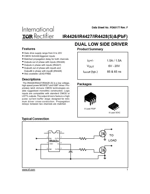
1.5A Dual High Speed
MOSFET Drivers CLM4426 / CLM4427 / CLM4428
FEATURES
•High Peak Output Current. . . . . . . . . . . . . . . . . . . >1.5A •Fast Switching. . . . . . . . . . . . . . . . . . . . . . . . . . t D = 40ns •Wide Operating Range. . . . . . . . . . . . . . . . . 4.5V to 18V •Matched Rise and Fall Times
•ESD Protected. . . . . . . . . . . . . . . . . . . . . . . . . . . . . . . 4kV APPLICATIONS
•Motor Controls
•Switch Mode Power Supplies
•Pulse Transformer Driver
•Class D Switching Amplifiers DESCRIPTION
The CLM4426 series are dual CMOS drivers are designed to drive capacitive, resistive and inductive loads switching 1000pF gate capacitances in under 30ns while providing low impedances in both the ON and OFF states to insure the MOSFET’s intended state will not be affected. All terminals are fully protected up to 4kV of ESD.
ORDERING INFORMATION
Part Logic Package Temperature CLM4426CP Inverting8 Pin PDIP0C to 70C CLM4426EP Inverting8 Pin PDIP-40o C to 85o C CLM4426CY Inverting8 Pin SOIC0o C to 70o C CLM4426EY Inverting8 Pin SOIC-40o C to 85o C CLM4427CP Noninverting8 Pin PDIP0o C to 70o C CLM4427EP Noninverting8 Pin PDIP-40o C to 85o C CLM4427CY Noninverting8 Pin SOIC0o C to 70o C CLM4427EY Noninverting8 Pin SOIC-40o C to 85o C CLM4428CP Differential8 Pin PDIP0o C to 70o C CLM4428EP Differential8 Pin PDIP-40o C to 85o C CLM4428CY Differential8 Pin SOIC0o C to 70o C CLM4428EY Differential8 Pin SOIC-40o C to 85o
C
ABSOLUTE MAXIMUM RATINGS
Supply Voltage. . . . . . . . . . . . . . . . . . . . . . . . . . . . . . . . . +22V Input Voltage, IN A or IN B. . . . . . . . . V DD +0.3V to GND-5.0V Maximum Chip Temperature. . . . . . . . . . . . . . . . . . . . +150o C Storage T emperature Range. . . . . . . . . . . . . -65o C to +150o C Lead Temperature (Soldering, 10 sec). . . . . . . . . . . . +300o C Package Thermal Resistance PDIP R θJ-A . . . . . . . . . . . . . . . . . . . . . . . . . . . . . . . 125o C/W PDIP R θJ-C . . . . . . . . . . . . . . . . . . . . . . . . . . . . . . . . 42o C/W SOIC R θJ-A . . . . . . . . . . . . . . . . . . . . . . . . . . . . . . . 250o C/W SOIC R θJ-C . . . . . . . . . . . . . . . . . . . . . . . . . . . . . . . . 75o C/W Operating T emperature Range
C Version . . . . . . . . . . . . . . . . . . . . . . . . . . . . 0o C to +70o C E Version . . . . . . . . . . . . . . . . . . . . . . . . . . . -40o C to +85o C Power Dissipation
Plastic. . . . . . . . . . . . . . . . . . . . . . . . . . . . . . . . . . . 1000mW SOIC . . . . . . . . . . . . . . . . . . . . . . . . . . . . . . . . . . . . 500mW
Static-sensitive device. Unused devices must be stored in conductive material. Protect devices from static discharge and static fields.Stresses above those listed under "Absolute Maximum Ratings" may cause permanent damage to the device. These are stress ratings only and functional operation of the device at these or any other conditions above those indicated in the operation sections of the specifications is not implied. Exposure to absolute maximum rating conditions for extended periods may affect device reliability.
AMBIENT TEMPERATURE (˚C)
PACKAGE POWER DISSIPATION
1000040025
150
1B-38
1251007550200600800PDIP
SLOPE = –8mW/˚C
SOIC
SLOPE = –4mW/˚C
(m W )
P D ELECTRICAL CHARACTERISTICS T A = +25o C with 4.5V ≤ V DD ≤
18V, unless otherwise specified.
Note: 1. Switching times are guaranteed by design.
ELECTRICAL CHARACTERISTICS
18V, unless otherwise specified.
Specifications measured over temperature range with 4.5V ≤ V DD≤
A • s e c
CROSSOVER ENERGY LOSS
418
1B-41
V DD
1614121086–9
10–8
10872
3
45
69NOTE: The values on this graph represent the loss seen by both drivers in a package during one complete cycle. For a single driver, divide the stated values by 2. For a single transition of a single driver, divide the stated value by 4.。