Wave Power Converter Pendulor with Hybrid H.S.T.
- 格式:pdf
- 大小:3.51 MB
- 文档页数:10
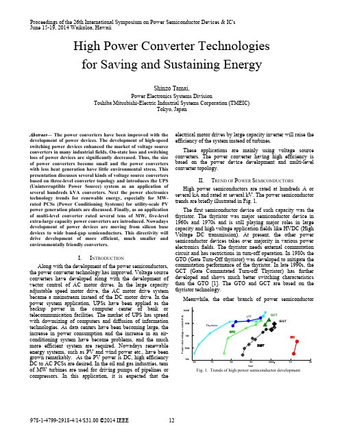
High Power Converter Technologies for Saving and Sustaining EnergyShinzo Tamai,Power Electronics Systems DivisionToshiba Mitsubishi-Electric Industrial Systems Corporation (TMEIC)Tokyo, JapanAbstract— The power converters have been improved with the development of power devices. The development of high-speed switching power devices enhanced the market of voltage source converters in many industrial fields. On-state loss and switching loss of power devices are significantly decreased. Thus, the size of power converters become small and the power converters with less heat generation have little environmental stress. This presentation discusses several kinds of voltage source converters based on three-level converter topology and introduces the UPS (Uninterruptible Power Source) system as an application of several hundreds kVA converters. Next the power electronics technology trends for renewable energy, especially for MW-rated PCSs (Power Conditioning Systems) for utility-scale PV power generation plants are discussed. Finally, as an application of multi-level converter rated several tens of MW, five-level extra-large capacity power converters are introduced. Nowadays development of power devices are moving from silicon base devices to wide band-gap semiconductors. This directivity will drive development of more efficient, much smaller and environmentally friendly converters.I.I NTRODUCTIONAlong with the development of the power semiconductors, the power converter technology has improved. Voltage source converters have developed along with the development of vector control of AC motor drives. In the large capacity adjustable speed motor drive, the AC motor drive system became a mainstream instead of the DC motor drive. In the power system application, UPSs have been applied as the backup power in the computer center of bank or telecommunication facilities. The market of UPS has spread with downsizing of computers and diffusion of information technologies. As data centers have been becoming large, the increase in power consumption and the increase in an air-conditioning system have become problems, and the much more efficient system are required. Nowadays renewable energy systems, such as PV and wind power etc., have been grown remarkably. As the PV power is DC, high efficiency DC to AC PCSs are desired. In the oil and gas industries, tens of MW turbines are used for driving pumps of pipelines or compressors. In this application, it is expected that the electrical motor drives by large capacity inverter will raise the efficiency of the system instead of turbines.These applications are mainly using voltage source converters. The power converter having high efficiency is based on the power device development and multi-level converter topology.II.T REND OF P OWER S EMICONDUCTORS High power semiconductors are rated at hundreds A or several kA and rated at several kV. The power semiconductor trends are briefly illustrated in Fig. 1.The first semiconductor device of such capacity was the thyristor. The thyristor was major semiconductor device in 1960s and 1970s and is still playing major roles in large capacity and high voltage application fields like HVDC (High Voltage DC transmission). At present, the other power semiconductor devices takes over majority in various power electronics fields. The thyristor needs external commutation circuit and has restrictions in turn-off operation. In 1980s the GTO (Gate Turn-Off thyristor) was developed to mitigate the commutation performance of the thyristor. In late 1990s, the GCT (Gate Commutated Turn-off Thyristor) has further developed and shows much better switching characteristics than the GTO [1]. The GTO and GCT are based on the thyristor technology.Proceedings of the 26th International Symposium on Power Semiconductor Devices & IC's June 15-19, 2014 Waikoloa, Hawaiidevice yielded IGBT (Insulated Gate Bipolar Transistor) in late 1980s. The IGBT is originated in the MOS-FET technology and power transistor technology. Then, for higher voltage with lower loss, IEGT (Injection Enhanced Gate Transistor) has been developed based on the IGBT technology [2].IGBTs are now very popular and used in many converters for capacity of several hundreds kW rated at several hundreds V. IGBTs also made very large markets of the voltage source type self-commutated converter for many fields. However, for fields requiring MW and kV, the GCT or the IEGT has advantages to make the converters since the IEGT is rated at 4.5kV-5.5kA and the GCT is rated at 6kV-6kA for example. With these high power semiconductor devices, the inverters rated at 20MVA or 30MVA can be made with small number of components.For future trends, wide band-gap semiconductors of SiC (Silicon Carbide) or GaN (Gallium Nitride) are now developed aiming better performance than the conventional Silicon based devices. For some specific application, some devices are now available in the market.III.C ONVERTER C IRCUIT T OPOLOGY By the spread of the power semiconductors, which can carry out self-commutation, the voltage source converters are widely in use. IGBT converters are used in many application fields. This chapter discusses the voltage source multi-level converter topology from the capacity of several hundreds kVA rated at several hundreds V.A.Two-level convertersThe conventional topology for power converter is a two-level configuration as shown in Fig. 2 (a). Fig. 2 (b) shows an illustration of one phase to neutral voltage (train of variable-width pulses) at the converter terminal using a two-levelAC systems, filtering using bulky reactors is required to suppress high frequency components.B.Three-Level converters:Diode Neutral Point Clamp (D-NPC) topologyThree-level neutral point clamped (NPC) converter topology was firstly proposed in 1980 [3]. One configuration of the three-level converter is shown in Fig. 3 (a). In each phase leg of the converter, three switching states are possible by adding a neutral point diode clamping state. Fig. 3 (b) shows an illustrative one phase to neutral voltage. The voltage pulse train tracks the sinusoidal waveform closer than in the case of a two-level converter by controlling the three states (+Udc, 0, -Udc) switching.As compared with the two-level converter, which has the same DC and AC voltage ratings, there are the following advantages about the three-level converter.•The voltage stress on each power switch is the half of the DC voltage.•The voltage variation (dv/dt) at the terminals is the half.Thus, in a circuit using a three-level topology, the voltage ratings of power semiconductors can be half of those in a two-level circuit. Additionally, there is a significant noise reduction (acoustic noise and electromagnetic interference)of a circuit using a three-level topology.C. Three-Level converters:Bidirectional-Switch Neutral Point Clamp (BS-NPC) topology Fig. 5 (a) shows the other configuration of the three-level converter. This circuit has bidirectional-switches in each phase between outputterminal and the neutral point of the DC circuit. The voltage stress of the switch of this circuit is also the half of the DC voltage and the voltage variation at theterminal is the half. The illustrative one phase to neutral voltage shows Fig. 5 (b) which is the same as the D-NPC circuit (Fig. 3 (b)). IV. U NINTERRUPTIVLE P OWER S UPPLY (UPS) Fig. 6 shows the main circuit configuration of the double conversion UPS. It comprises a PWM-based rectifier, a PWM inverter, a bidirectional chopper circuit, a DC-link circuit andinput and output LC filters. The UPS has a transformer-lessdesign, which promotes reduction of losses and henceincreases the overall efficiency. In the UPS, instead of using a conventional two-level circuit topology, a three-levelconfiguration is employed to achieve higher efficiency, higher performance and higher reliability in online UPS systems. A. D-NPC converter UPS [4]Despite of the fact that a three-level converter presents higher number of components, the overall efficiency actually increases in comparison with the traditional two-level topology. Because multilevel converters promote lower voltage stresses on power semiconductors, voltage ratings of transistors and diodes can be lowered without compromise performance and reliability. Power semiconductors with lower voltage ratings feature superior conduction and switching characteristics for any given current. Owing to this feature, the proposed UPS (three-phase, nominal voltage class of 400V) using the NPC three-level topology can be structured by 600V-IGBTs. In a traditional design using two-level topology, a UPS with the same specification would require a 1200V-IGBT. The saturation voltage for a 1200V- and a 600V-IGBT in same generation from the same manufacturer is almost the same. However, in terms of switching characteristics, a 600V-IGBT exhibits superiority.Considering both types of losses in a UPS, the three-levelNPC concept realizes a substantial improvement of the overallpower conversion efficiency. Despite of the fact thatconduction losses almost doubles, switching losses aredramatically reduced by a three-level topology. Efficiencies of the proposed UPS are measured for variousload percentages to show the improvement in power losses.The 225-kVA UPS efficiency curve is shown in Fig. 7. In comparison with a conventional UPS, the UPS with three-level D-NPC circuit has superior efficiency due to the three-level-based circuit topology. Note that the efficiency curve exhibits flatness for load percentage of about 40 percent and higher. B. BS-NPC converter UPS [5] A three-level BS-NPC type converter also uses twice the number of IGBT modules. However multilevel converterspromote lower voltage stresses on power semiconductors thatreduce the losses of conversion. In a three-level BS-NPC type circuit, switching losses accounted for nearly 53% ofFig. 6. Main circuit configuration of the UPSwith a two-level topology.Efficiency curves for a 500kVA system are shown in Fig.8. In comparison with a conventional UPS, the BS-NPC UPS exhibits green-level efficiency due to the three-level based circuit topology. The efficiency curve exhibits flatness for a load percentage of 25% and higher. The maximum efficiency is over 97%. For a load percentage above 25%, efficiency is nearly 97%. Thus, it is expected to achieve high efficiencies in actual use and even in multiple module systems where the individual load percentage for each UPS is normally low. The external appearance of a 500kVA-module is shown in Fig. 9 [6].V.P OWER C ONDITIONING S YSTEM FOR MW-R ATEDP HOTOVOLTAIC G ENERATIONThis chapter introduces the PE technology trends for renewable energy, especially for MW-rated PCSs for utility-scale PV power generation plants.A.PV generation capacity increase in JapanIn order to promote renewable energy, the government of Japan started the feed-in tariff scheme in 2011. The scheme includes, photovoltaic, wind, geo-thermal and small-scale hydraulic generations. By the statistics of Japan Photovoltaictriple compared beforeand after introduction of the scheme[7]. The statistics also indicates a considerably large increasein utility scale PV generation for non-residential use or forpower generation business in addition to constant capacityincrease for domestic use. The increase in 2009 was madebecause of another promotion scheme for residential PVgeneration.This remarkable step change is considered also affected bythe experiences after the Great East Japan Earthquake inMarch 2011. The earthquake stopped many centralizedgeneration and transmission facilities and resulted in electricpower shortage for long time. Then, the concept of “localgeneration and local consumption” has been developed forsecure electric power supply in Japanese people. For localgeneration, the renewable energy is suitable because of itsnature.B.Requiremets to PV PCSAs indicated in Fig. 10, non-residential PV generationincreased the capacity very much. For such generation plant,large-capacity PCSs are required to convert the DC power ofphoto voltaic cells to the AC power in the AC power grid. Inorder to meet the demand, a PCS rated at 500kW has beendeveloped as shown in Fig. 11 (a). One of most importantfactor of PCS for PV generation is the efficiency since higherefficiency means better economics in the feed-in tariff scheme.In order to operate the PV plant with high system efficiency,the following factors are necessary to be considered.•High efficiency in DC to AC conversion•Minimum power loss in the DC network from the PVcells to the PCS•Small restrictions on MPPT control of the PV cells.The 500kW PCS has been developed considering thesefactors [8]. In addition to requirements for electricalperformances, from practical viewpoints, the rapid PVcapacity increase requires to save installation works at plantsites. Then, the PCSs are usually placed in an outdoor typecontainer as shown in Fig. 11 (b) and installed near the PVpanels at generation plants.Fig. 9. External appearance of a 500kVA UPSC.High PCS efficiency by muti-level technologyThe 500kW PCS applies three-level BS-NPC circuit topology [9]. In this case, the multi-level inverter technology contributes to improve inverter efficiency and wide operation range of DC voltage output from the PV cells.The BS-NPC topology offers smaller switching loss of the IGBT as shown in Fig. 12 compared with the two-level inverter. The feature results in one of the highest conversion efficiency in the world as shown in Fig. 13.D.High system efficiency by wide operation rangeThe developed PCS also has feature in the wide operation range, which is preferable for the PV generation plant since it offers higher system efficiency because of smaller DC network loss and wide MPPT (Maximum Power Point Tracking) range [10].The PV cell output voltage reaches around 1000V these days at the light load condition. The higher voltage is preferable to reduce the conduction loss in the DC network from the PV cell to the PCS. The PCS is required to handle such high cell voltage. Then, the PCS with the three-level topology suitable since it can handle two times higher DC voltage than the conventional two-level converters when the IGBT of same voltage rating is used. The 500kW PCS has the current overload capability to handle the peak load. Then, the operation range fully covers the PV cell module output characteristics.VI.L ARGE C APACITY D RIVE I NVERTERS In oil and gas industries, many compressors or pumps of large capacity are working. In gas industries, large compressors rated at tens of MW are used for pipeline transportation or for liquefaction to LNG (Liquefied Natural Gas). In this range of capacity, conventionally, they are drivenby the turbines. Meanwhile, for better operation efficiency and fossil fuel saving, electrification trend is spreading in various industrial fields. In order to expand the trend to large-capacity compressors, the motors and drive inverters are also required to handle the capacity range of tens of MW.The combination of the high power and high-speed semiconductors greatly contributed to realize large-capacity drive inverters. They are now already available in the market and contributing for oil and gas industry. This chapter introduces technologies of large-capacity drive inverters.A.Circuit topologyThe D-NPC converter topology has advantages for large capacity drive inverters. The first advantage is the high voltage output. The D-NPC topology can output higher voltages compared with two-level inverters widely used for general purpose in rather low voltage applications. When, the power semiconductor devices of same voltage ratings, the three-level inverter can output two times higher voltage than(a)500kW PCS(b) PCSs installed in container for 1MW systemFig. 11. 500kW PV PCS and 1MW system120%Fig. 13. Efficiency characteristics of developed PCSthe two-level inverter. The five-level inverter shown in Fig. 14(a) outputs four times higher voltage as shown in Fig. 14(b). When the IEGT or the GCT is applied to this circuit topology, the five-level drive inverter is rated at 20MW or 30 MW [12] [13] [14]. The capacity is suitable to drive large-capacity compressors. Fig. 15 shows 20MW and 30MW-rated drive inverter.The second advantage is the smooth voltage waveform. As shown in Fig. 16 (a), the phase-to-phase voltage of the five-level inverter has nine levels of voltage steps approaching sinusoidal waveform. The inverter output voltage level N is defined for phase to neutral. Then, for phase to phase, the number of voltage step counts as 2N-1 based on the theory. The five-level inverter, then, can output nine-level voltage in phase to phase. This feature is friendly to motors since harmonic current components are smaller than those from the two-level inverters.B. Advanced controlThe high-speed semiconductors in digital control circuits realized implementation of an advanced real-time control to eliminate low order harmonics from its voltage output as shown in Fig. 16 (a). The frequency components are analyzed as shown in Fig. 16 (b) [15].(a) 20MVA drive inverter with IEGT(b) 30MVA drive inverter with GCTFig. 15. Examples of extra-large drive inverterseliminated from the pulse pattern. To obtain the pattern, it is necessary to solve multiple non-linier equations. These days even with a general PC (Personal Computer), digital computations can be done to solve the equations for sufficient numbers of cases for inverter operation status. Then, the calculation results are installed in memories of the digital control as look-up tables and referred on line to generate the pulse pattern. This type of control technology is widely used and field proven by large-capacity inverters for other application fields. [16]The elimination of low harmonics components contributes smooth rotation of compressors. The large compressor system consists of long train of machines with a long axis and has mechanical resonance frequency usually lower than tens of Hz. Considering the characteristics of large-capacity compressors, the advanced control outputs the voltage waveform can be tuned as consisting of only frequency components different from the resonance frequency.VII.C ONCLUSIONThe paper introduced the developments in the power semiconductors first. These technology developments have been applied in the large power converters from hundreds of kVA to tens of MW.The multi-level NPC converter applications based on the high performance power semiconductors are introduced for UPS systems, for renewable power generations and for oil and gas industries. The multi-level converter technology contributes high voltage output and high efficiency and is suitable for saving and sustaining energy resources.The development of semiconductors still continues and promotes further development of the high power converters.A CKNOWLEDGMENTThe author thanks the Organizing Committee and Technical Committee of the 26th IEEE ISPSD 2014 Conference for offering me a good opportunity to introduce trends of high power converter technology. The author also thanks Dr. Gourab Majumdar of Mitsubishi Electric Corporation for informing me the good opportunity. The author also thanks Mr. Hidehiko Kikuchi, Corporate Vice President of TMEIC, Teruo Yoshino, Senior Fellow of TMEIC who gave me many suggestions and support. The author also thanks friends who supported the converter development in many aspects including project management, design, assembly and evaluation test.R EFERENCES[1]M. Yamamoto, K. Satoh, T. Nakagawa,A. Kawakami, ”GCT (gatecommutated turn-off) thyristor and gate drive circuit,“ IEEE PESC 98, Vol.2, pp. 1711 - 1715, 1998.[2]M. Kitagawa, I. Omura, S. Hasegawa,T. Inoue,A. Nakagawa, “A 4500V injection enhanced insulated gate bipolar transistor (IEGT) operating in a mode similar to a thyristor,” Electron Devices Meeting, IEDM '93, 1993.[3] A. Nabae, I. Takahashi, H. Akagi, “A new neural-point-clamnpedPWM inverter,” IEEE Trans. Ind. Appl. Vol. IA-17, No. 5, pp. 518 - 523, 1981.[4] E. K. Sato, M. Kinoshita, Y. Yamamoto, T. Amboh, “Redundant high-density high-efficiency double-conversion uninterruptible power system,” IEEE Trans. Ind. Appl. Vol. 46, No. 4, pp. 1525 - 1533, 2010.[5]T. Lee, M. Kinoshita, K. Sanada, “High-efficiency large-capacityuninterruptible power supply using bidirectional-switch-based NPC multilevel converter,” ICPE2011-ECCE Asia, pp. 2100 - 2105, 2011. [6]K. Ohnishi, H. Masunaga, K. Matsuoka, K. Sanada, “Innovation ofhigh efficiency UPS for energy saving,” 2011 IEICE- Japan Society Conference, BS-5-2, pp.S23 – S24, 2011.(In Japanese)[7]http://www.jpea.gr.jp/en/statistic/index.html, Web page of JapanPhotovoltaic Power Generation.[8]T. Amboh, E. Ikawa and R. Inzunza, “Relevant Aspects in Designing aPhotovoltaic Inverter for Industrial and Commercial applications,”IPEC2010-ECCE Asia, pp. 688 - 693, 2010.[9]R. Inzunza, H. Yamaguchi, E. Ikawa, T. Sumiya, Y. Fujii, A. Satoh,“Design and Development of a 500kW Utility- Interactive Switch-Clamped Three-Level Photovoltaic Inverter,” ICPE2011-ECCE Asia, pp. 1627 - 1631, 2011.[10]K.S. Lee, Y. Fujii, T. Sumiya, E. Ikawa, “Development of a 250kW PVPCS and adaptive MPPT method,” IPEC2010-ECCE Asia, pp. 2598 - 2602, 2010.[11]T.Yoshino, H. Masuda, H. Hosoda, M. Tsukakoshi, M. A. Mostafa, L.Ben-Brahim, “High-reliability extra-large motor drives for oil and gas industry,” IEEE GCC2013, 159 - 164, 2013.[12]D. Yoshizawa, K. Takao, M. Mukunoki, Y. Shimomura, “The largeCapacity 5 level GCT Inverter for OIL & GAS plant application,” 2008 IEE- Japan IAS Conference, pp.I359 - I362, 2008.(In Japanese) [13]M. Tsukakoshi, M. A. Mamun, K. Hashimura, H. Hosoda and S. C.Peak, “Introduction of a large scale high efficiency 5-level IEGT inverter for oil and Gas industry,” IEEE ECCE2010, pp. 1261 - 1265, 2010.[14]H. Hosoda, S. Peak, “Multi-level converters for large capacity motordrive,” IPEC2010-ECCE Asia, pp. 516 - 522, 2010.[15]M. Tsukakoshi, M. A. Mamun, K. Hashimura and H. Hosoda, J.Sakaguchi, L. Ben-Brahim, “Novel torque ripple minimization control for 25MW variable speed drive system fed by multilevel voltage source inverter,” 39th Turbomachinary Symposium, pp. 193 - 200, 2010. [16]M. Tsukakoshi, M. Mukunoki and R. Nakamura, “High performanceIEGT inverter for main drives in the steel industry,” IPEC2005, S15-2, 2005.。

一种适用于光伏发电系统的新型两相交错并联Boost变换器程千;张代润;程满;黄钰【摘要】针对传统两相交错并联Boost变换器输出电压增益较低,开关器件的电压应力较高的缺陷,文章在传统两相交错并联Boost变换器的基础上增加了2个二极管和3个电容,并进行了结构上的改进.在此基础上分析了占空比D>0.5时的工作原理,结果表明,新拓扑具有传统拓扑输入电流纹波小的优点,并且在相同的占空比下,其输出电压增益为传统拓扑的4倍,同时开关管和二极管的电压应力也得到了明显减小.最后,通过Matlab/Simulink仿真验证了理论分析的正确性.【期刊名称】《可再生能源》【年(卷),期】2015(033)011【总页数】5页(P1614-1618)【关键词】交错并联Boost变换器;电流纹波;电压增益;电压应力【作者】程千;张代润;程满;黄钰【作者单位】四川大学电气信息学院,四川成都610065;四川大学电气信息学院,四川成都610065;四川大学电气信息学院,四川成都610065;四川大学电气信息学院,四川成都610065【正文语种】中文【中图分类】TM46随着社会的快速发展,对能源的需求与日俱增,传统燃料不仅总量有限,还造成了严重的环境污染。
可再生能源的利用成为一种趋势,其中,太阳能光伏发电以其可靠、安全、运行成本低、应用范围广等优点可以有效解决当今社会的能源危机问题[1],[2]。
在光伏发电系统的实际应用中,系统的输出功率容易受到外界环境因素的影响,所以系统中往往需要采用最大功率跟踪技术,而DC/DC变换器是其重要的组成部分。
传统的Boost变换器具有许多优点,比如结构简单;输入电流连续;提升输出电压以弥补光伏电池输出电压低的劣势;在故障情况下二极管可以防止电流回流,从而避免系统损坏。
因此它被广泛应用于光伏电池最大功率跟踪电路中[3]。
由于传统Boost变换器升压能力有限,不适用于对电压要求较高的场合,并且开关管和二极管的电压应力与其输出电压相等,相对较高,这就增加了系统的成本,降低了系统工作的可靠性,另外其输入电流纹波较大还会减短光伏电池的使用寿命。

a numerical study of wave energy converter
海浪能转换器已经成为一种新的、可再生的能源来源。
在这方面,数值模拟成为了一种重要的研究手段。
本文通过数值模拟的方法,研究了海浪能转换器的性能。
首先,我们需要建立一个数学模型。
在海浪能转换器中,液体的运动可以通过Navier-Stokes方程来描述。
同时,海浪的影响可以通过波浪方程来考虑。
在这个模型中,我们还需要定义边界条件和初始条件。
通过这个模型,我们可以预测海浪能转换器在不同条件下的运动情况。
在这个模型的基础上,我们可以进行不同的数值模拟。
例如,我们可以通过计算流体动力学方法来研究海浪能转换器的流场。
通过这种方法,我们可以计算出流体的速度、压力等参数,进而研究海浪能转换器受到海浪作用时的响应情况。
此外,我们还可以通过有限元分析方法来研究海浪能转换器的动力学性能。
在这种方法中,我们可以将海浪能转换器看做一个复杂的结构体系,通过有限元分析计算出它的结构响应、振动频率等参数。
这些参数可以帮助我们优化海浪能转换器的结构设计,提高其性能。
总之,通过数值模拟的方法,我们可以更深入地研究海浪能转换器的性能,并且优化其设计,提高其能量转换效率。
这对于实现海洋能源的可持续利用具有重要意义。
- 1 -。

第26卷第9期2006年5月文章编号:0258—8013(2006)09—0094—05中国电机工程学报ProceediIlgs、,b1.26No.9May2006@2006Cllin.Soc.五0rElec.EngofmeCS髓文献标识码:A中图分类号:TM624学科分类号:470.40一种新颖的升压型电压调整器一两相交错并联耦合电感BOOST变换器胡庆波,瞿博,吕征宇(浙江大学电力电子国家专业实验室,浙江省杭州市310027)ANoVelStep-upV】王M——Two—phaseHUInterleaVedCoupled-boostConVerterZheng—yuQing-bo,QUBo,LU(NationalKeyLabomtoryofPowerElec仃onics,ZhejmgUIliversity,zheji柚gPmvince,H柚gzhou310027,Cllina)islongersoABsl’I认C1j’11leAsfornatIlrallifeOfbanerycellth柚low.关键词:升压型电压调整器,交错并联,耦合电感,有源钳位batterygroupusedinseries,butbatteryceUv01tageismisproblem,tllispaperin廿oducestwo—phaseintedeaVedcanastep—upcircllit,namedcoupled—BoostconVener,and0引言随着蓄电池的大量使用,蓄电池的使用寿命越dif托rentoutputVoltageofbeacquiredbych柚gingtIlmsisratioaco叩ledinductor.Tho—phasela唱edutycyclebecaIIsecanboostconverteroperatesatVoltagegain来越得到人们的关注。
目前,蓄电池在使用过程中通常采用串联的工作方式,这种方式下串联组内蓄电池均以同样大小的电流进行充放电。

IM205609/2014REV00 POWER WAVE® ADVANCED MODULE Spare Parts (1)POWER WAVE® ADVANCED MODULE (1)Miscellaneous Items (1)Assemblies overview (2)Figure 1: Case Front Assembly & Sides (3)Figure 2: Top Extrusion Assembly, Roof & Case Sides (4)Figure 3: Base Extrusion Assembly & Fun (5)Figure 4: Switch Board and Bracket Assembly (6)Figure 5: Rear Panel Assembly (7)Electrical Schematic (8)POWER WAVE® ADVANCED MODULE 11935 (8)Lincoln Electric Bester Sp. z o.o.ul. Jana III Sobieskiego 19A, 58-263 Bielawa, Polandwww.lincolnelectric.euSpare PartsSP11935 Rev0007/03POWER WAVE ® ADVANCED MODULESub Assembly Number/Figure Number1 2 3 4 5M i s c e l l a n e o u s I t e m sC a s e F r o n t A s s e m b l y & S i d e sT o p E x t r u s i o n A s b l y , R o o f &C a s e S i d e sB a s e E x t r u s i o n A s b l y & F a nS w i t c h B o a r d & B r a c k e t A s s e m b l yR e a r P a n e l A s s e m b l yCODE NO. 11935 1 1 1 1 1 1Miscellaneous ItemsThese Items are not illustred Item Description Part Number QTY 1 2 3 4 5 6 ARC SENSE LEAD M20023-1 1 X CAM LOCK TERMINAL ADAPTER M21433-2 2 XAssemblies overviewFigure 1: Case Front Assembly & SidesNumber QTY 1 2 3 4 5 6 Item Description Part1 Case Front Welded Assembly L12761-2 1 X2 Nameplate L16050 1 XAssembly M13896-7 1 XStud3A OutputCover M24789 1 X4A ReceptacleAssembly S16656-4 2 XTerminal5A Output6 Nut T3960 2 XCover G6864 2 X7A OutputStudLead M19651-7 1 XPower12 PositiveLead M19651-8 1 XPower13 Negative14 Plug & Lead Assembly (Not Shown) M24907 1 X16A H.F. Cap Discharge P.C. Board G7372-[ ] 1 XReceptacle S18657 1 X25A SquareFlangeFigure 2: Top Extrusion Assembly, Roof & Case SidesItem Description PartNumber QTY 1 2 3 4 5 6 2A CornerCap L13138 4 X3A Front Mounting Bracket Assembly S28458 1 X3B Rear Mounting Bracket Assembly S28459 1 XBracket S28375 1 X5A Locking6A Roof L12763-3 1 XSide L12752-2 1 XCase10A RightSide L12752 1 XCase11A LeftFigure 3: Base Extrusion Assembly & FunItem Description PartNumber QTY 1 2 3 4 5 6 1A BaseRail M21251-2 2 X2A Base L12785-3 1 X4A Quick Lock Foot S28070 4 X8A CornerCap L13138 4 XAssembly M22853 1 X18A FanBracket M24905 1 X18B FanFigure 4: Switch Board and Bracket AssemblyItem Description Part Number QTY 1 2 3 4 5 6 1 HeatsinkBase L12743-2 1 X2 P.C. Board Heatsink Assembly S29825-[ ] 1 X2A Diode S25520-1S 2 X13A Hi-Freq Transformer Assembly M24123 1 X15A Background Choke Assembly M24942 1 X16A RectifierModule M15482-1 1 XFigure 5: Rear Panel AssemblyItem Description PartNumber QTY 1 2 3 4 5 6 Panel G5016-3 1 X1 Rear5 Arclink Cable Assembly, Includes: M22438 1 X6 Sync Tandem Cable Assembly, Includes: M22432-1 1 X7A Solenoid M17294-8 1 X8 Arclink Receptacle Assembly, Includes: M20124-4 1 XElectrical SchematicPOWER WAVE® ADVANCED MODULE 11935。
Buck-Boost Converters*******Zhengzhou university institute of electrical engineering , Zhengzhou 450001Abstract:This section has presented and analyzed a buck–boost converter (Fig. 2.28). The topological changes have been presented and a discussion of the state space has shown a modeling process (averaging), which can be used to design the converter. This process models a linear time-varying structure in a relatively simple way so that significant design insight can be obtained. The small signal model that was presented can be used to analyze the stability and the input-to-output signal attenuation of the buck–boost converter.Keywords:buck–boost converter nonlinear topology small signal transfer functionI INTRODUTIONSwitching power is widely used in household appliances, computers, communications, control, and other equipment. The development of modern electronic communication technology more and more be high to the requirement of power supply. In the field of many voltage change, the input voltage changes in a wide range . Here , the buck-boost converter are introduced and analyzed.II MAINA schematic of the buck–boost converter circuit is shown below in Fig. 2.28. The main power switch is shown to be a bipolar transistor, but it could be a power MOSFET, or any other device that could be turned on (and off) in a controlled fashion. This converter processes the power from a DC-biased source (high-voltage ripple) to a DC output (containing low-voltage ripple). The DC output voltage value can be chosen to be higher or lower than the input DC voltage. Note: The output load is represented by a resistor, RL , but in real life can be something much more complicated. In a general sense, this circuit processes power from input to output with “square wave” technology, that is, the circuit produces waveforms that have sharp edges. The waveforms in Fig. 2.29have asquare-wave (or semi-square-wave) appearance and are indicative of current waveforms in a typical DC-DC converter. In fact, the iL waveform is in a similar shape as the inductor (L) current in the buck–boost converter of Fig. 2.28, iDcan represent the diode current, and iC , the capacitor current. The operation of this converter is nonlinear and discrete; however, it can be represented by a cyclic change of power stage topologies. The three topologies for this converter, the equations for those topologies, and the small-signal transfer functions are presented in this section.FIGURE 2.28 Buck–boost converter.FIGURE 2.29 Typical current waveformsin abuck–boost converter.III CIRCUIT ANALYSISThe buck–boost converter has cyclic changes in topology due to the switching action of the semiconductor devices. During a cycle of operation, the main power switch is turned on and off; the diode responds to this by switching off and on.IV CONTINUOUS-CURRENTMODEA.nonlinearFigure 2.30illustrates the topology where the main power switch is on and the diode is reverse-biased; thus, it is off. For the purpose of illustration the semiconductor devices are assumed to be ideal.There are two independent state variables that contain the information describing the operation of this circuit: the inductor current, iL , and the capacitor voltage, vC. Two differential equations in terms of these variables, the output voltage, vO, and the source voltage, vS , for the designated Topology 1 are shown below.(2.23)(2.24)Please note that the inductor is receiving energy from the source and being charged up, while the capacitor is being discharged into the output load, RL , and the output voltage is falling. Figure 2.31shows the change in topology when the main power switch turns off. The inductor maintains current flow in the same direction so that the diode is forward-biased. The differential equations for the designated Topology 2 are shown below. Please note that the inductor is transferring the energy it has obtained from the source into the capacitor; the capacitor is being charged up as the inductor is being discharged, and the output voltage is rising.FIGURE 2.30 Topology 1 for the buck–boost converter.FIGURE 2.31 Topology 2 for the buck –boost converter. (2.25) (2.26) These four linear time-invariant differential equations describe the state of the buck –boost converter. The power stage analysis is linear for each interval; however, for the complete operational cycle, it becomes a piecewise linear problem. The on-time or off-time of the main power switch may vary from cycle to cycle, further complicating the analysis. Various modeling schemes have been proposed using nonlinear techniques that would in essence “combine” these equations. Basically there are two approaches: numerical (universal) and analytical (mathematical) techniques [1, 2]. In analytical techniques, a closed-form expression representing the operation of the converter is obtained, enabling a qualitative analysis to be performed [1]. The numerical techniques use various algorithms to produce an accurate quantitative result. However, simple relations among the system parameters are not easily obtainable. Numerical techniques are not to be considered at this time, because the desire at this point is to obtain a closed-form solution from which a considerable amount of design insight can be obtained. B.Analysis methodAnalytical techniques can be divided into two different system descriptions, discrete and continuous. The discrete system description makes no simplifying assumption on the basis of converterapplication. This description could beused in any application where the linearization of a periodicallychanging structure is sought. Thismethod is accurate, but very complicated. The derived expressions are complex andcumbersome,which impedes its practical usefulness, and physical insight into the system operation is not easily obtainable. An important continuous analytical technique is the averaging technique by Wester and Middlebrook [3]. It is easy to implement and gives physical insight into the operation of a buck –boost converter. Through circuit manipulation, analytical expressions were derived to determine the appropriate expressions. Middlebrook and Cúk [4, 5] modified the technique to average the state space descriptions (variables) over a complete cycle. Shortt and Lee [6–8] used a discrete sample of the average state space representation to develop a modeling technique that would enable a judicious control selection to be made. Vorpérian et al. [9] developed an equivalent circuit model for a pulse width modulation (PWM) switch that can be used in the analysis of this converter. For the averaging technique each interval in the cycle is described by its state space representation (differential equation). Figure 2.32shows the waveform of the continuous,instantaneous inductor current (that is,iL does not equal zero at any pointin time) and the average inductorcurrent for the buck–boost converter(Fig. 2.30). The instantaneous currentis cyclic with a time period equal to TPs;the main power switch is on for TONs andoff for TOFFs. The equations areaveraged to give a single period representation, as shown below:(2.27)(2.28)FIGURE 2.33 Inductor current perturbation.DC conditions:AC conditions:The equtionform eqution(2.29).Note:from FIGURE 2.28,,That is:(2.33)Another method that is utilized to extract the small signal model is to realize an equivalent circuit model from Eqs. (2.27) and (2.28). Figure 2.34is the average circuit model of the buck–boost converter.FIGURE 2.34 Average circuit model of the buck–boost converter.V DISCONTINUOUS-CURRUTMODEFigure 2.36shows the waveform of the discontinuous inductor current for the buck–boost converter (Fig. 2.30). Note that the inductor current is equal to zero for TF2s. This results in an additional (third) topology change, shown in Fig. 2.37.FIGURE 2.36 Discontinuous inductor current.FIGURE 2.37 Topology 3 for the buck –boost converter (discontinuous inductor current) . Since the inductor current is zero for this portion of the switching cycle, there is only one state equationthat can be determined. (2.35)This equation indicates that the capacitor is now discharging its energy into the load resistor, RL, and the output voltage is falling:(2.40)FIGURE 2.38 General form of discontinuous inductorcurrent.VI SMALL SIGNAL TRANSFERFUNCTIONSThe analysis done in the previous section enables the development oftransfer functions that describe the buck –boost converter stability performance and input to output signal attenuation. The transfer functions are illustrated in Fig. 2.40. This figure assumes there is only one feedback (the output voltage) loop; for morecomplicated feedback schemes, please see Refs. 7 and 8.The continuous-current mode transferfunctions are derived by using the Laplace transform to solve for the output voltage and duty cycle variations in Eqs. (2.31) and (2.32). Equation(2.42) is used to derive the discontinuous-current mode transfer functions.FIGURE 2.40 Block diagram of transfer functions for the buck –boost converter: (a) continuous-current mode; (b)discontinuous-current mode.VII COMPONENT SELECTIONThe component values can be chosen based on several constraints. The constraints that are to be discussed here are not exhaustive, but are only mentioned to provide an introduction into the selection process. Some component values can be based on an arbitrary selection. For example, the frequency of the conv erter is the designer’s choice. As the frequency rises, the volume of the inductor (which is usually the biggest component in the converter) decreases and its temperature rises. The component value can be selected based on a given frequency value, which is assumed to be optimized based on the previously mentioned constraints. However, the frequency value can also be chosen based on experience. There is to be no discussion on the optimization of the switching frequency in this section; please see Ref. 13 for a detailed explanation of the process to optimize the converter switching frequency. Thus, an assumption made at this point is that the switching frequency has been selected.SUMMARYThis section has presented and analyzed a buck–boost converter (Fig. 2.28). The topological changes have been presented and a discussion of the state space has shown a modeling process (averaging), which can be used to design the converter. With the continuous development of the CPU, the emergence of new technology is also in constant. We should continuously research and improve these new technologies, to promote its application soon.REFERENCE [1] Owen, H. A., Capel, A., and Ferrante, J. G.,Simulation and analysis methods for sampled power electronic systems, in IEEE Power Electronics Specialists Conference Record,1976, 45–55.[2] Middlebrook R. D. and Cúk, S., A generalunified approach to modeling switching-converter power stages, in IEEE Power Electronics Specialists Conference Record,1976, 18–34.[3] Lee, F. C. and Shortt, D. J., Improved modelfor predicting the dynamic performance of high bandwidth and multiloop power converters, inPOWERCON 11 Record,1984, E-3, 1–14.[4] Shortt, D. J. and Lee, F. C., Extensions ofthe discrete-average models for converter power stages, in PESC Record,1983, 23–37;IEEE Trans. Aerospace Electron.Syst.,AES-20(3), 279–289, 1984.[5] 解妮娜,王志强。
WaveStation™High Performance andSignal FidelityHigh performance hardware enables WaveStation to create accurate stable waveforms. High sample rate and resolution combined with low jitter and harmonic distortion means waveforms seen on the display are accurately created and outputted by the hardware.Extensive Waveform Library Easily create basic sine, square, ramp, pulse, and noise waveforms. In addi-tion, access over 40 advanced arbitrary waveforms preloaded on WaveStation. Edit waveforms using the WaveStation PC software with point-by-point manu-al waveform design or waveform draw-ing tools. Use digital filtering tools for advanced waveform creation.Connectivity and CommunicationWith standard USB and GPIB connec-tivity it is easy to control WaveStation remotely or integrate it in to a test system. All necessary I/O for synchro-nization can be accessed on the rear panel. A front panel USB port provides an easy way to save waveforms. Simple, Fast Waveform CreationThe intuitive front panel provides easy access to waveforms, modulation and operating modes. The large display shows all relevant waveform parame-ters and waveform shape. Included PC software provides a graphical interface for quickly modifying waveforms with point-by-point editing, digital filtering and waveform drawing tools.Key Features•H igh performance with 14-bit resolution, up to 500 MS/s sample rate and up to 512 kpts memory •2 channels on all models•L arge color display for easy waveform preview•O ver 40 built-in arbitrary waveforms•L inear & Logarithmic sweeps and burst operation•U SB and GPIB connectivity •G raphical waveform editing software for PC With 5 basic signal types, and over 40 built-in arbitrary waveforms the WaveStation is a versatile waveform generator. A variety of modulation schemes, intuitive waveform editing software and remote control capabilities, enable versatile waveform generation of waveforms up to 160 MHz. The large color display and simple user interface make it easy to generate a wide range of waveforms.2Variety of Modulation SchemesBuilt-in modulation capabilities include AM, PM, FM,ASK, PSK and FSK. View the modulated waveform onthe display and see how it changes when varying out-put frequency, carrier waveform or modulation type.1.Dual OutputTwo synchronous outputs foradditional waveform flexibility andability to create differential wave-forms.2.Color DisplayLarge display provides a single viewto see waveform preview, parametersand menus with a single glance.3.Waveform PreviewHelpful display provides preview of thewaveform to be generated.B ConnectivityFront panel USB port to quickly saveand transfer waveforms.5.Display MenuQuick access to various parameterswith one touch to soft button on thefront panel.546322343Graphical Waveform CreationEasily create and edit waveforms on the PC withmathematical operations, filters, and point-by-point editing or draw a waveform with a mouse. Transfer waveforms to WaveStation over USB and view it on the large display. Additionally, connecting a WaveAce oscilloscope to the same PC enables seamless transfer of real world signals from oscilloscope to the WaveStation.106. O n-Screen Parameter ReadoutView all relevant parameters at the same time on a single screen.7.Quick Waveform AccessDedicated, backlit buttons for quick access to the most common waveforms.8.Easy to Use Front PanelIntuitive front panel allows for quick waveform parameter entry and editing.9.Adjustable HandleEasily adjust handle for easy transport, optimal viewing and comfortable use.10.ConnectivityAll necessary I/O for synchronization can be accessed from rear panel.19781567894WaveformsSine, Square, Ramp, Pulse, Noise, Arbitrary: Stairup, Stairdown, Positive Pulse, Negative Pulse,Up Ramp, Down Ramp, Sinc, Gaussian, LogFall, LogRise, Sqrt, TwoTone, etcWaveform Characteristics5201220222052308231223162Modulation, Sweep, Burst CapabilitiesAmplitude Modulation Source Internal / ExternalCarrierSine, Square, Ramp, Arbitrary (except DC)@ Max Sampling Rate 3.90625 MHz Memory Size 4 k x 12 bitFrequency Modulation Source Internal / ExternalPhase Modulation Source Internal / ExternalFSK Modulation Source Internal / ExternalASK Modulation Source Internal / ExternalCarrierSine, Square, Ramp, Arbitrary (except DC)Sweep Carrier Sine, Square, Ramp, Arbitrary (except DC)Type Linear / LogarithmicDirection Up / DownBurst Trigger SourceManual, External or Internal6201220222052308231223162Channel CharacteristicsOutput Connector BNCOutput Impedance 50 Ω, High ImpedanceExternal Clock Pulse Width > 50 ns, not adjustableOutput Impedance 50 Ω (typical)Maximum Frequency 1 MHzOutput Connector Through Rear Panel Ext Trig / Gate / FSK / BurstGeneral CharacteristicsStandard InterfaceUSB Host, USB Device and GPIB (IEEE 488)Front Panel Connectors Output BNC and USB hostRear Panel Connectors BNC and USB device7201220222052308231223162General Characteristics (cont’d)Output Connector BNCRange (DC) - Ch2Waveform Output Impedance 50 Ω (typical), High ZProtectionShort-circuit protectionPowerVoltage100 - 240 V rms (± 10%), 50 / 60 Hz 100 - 120 V rms (± 10%), 400 HzConsumption (nominal)50 W MaxEnvironmentTemperature - Operating 0° C to 40° C Temperature - Storage-20° C to 60° CHumidity Range - Operating 5% to 90% relative humidity (non-condensing) up to +30° CUpper limit derates to 50% relative humidity (non-condensing) at +40° C Humidity Range - Non-operating 5% to 95% relative humidity (non-condensing) as tested per MIL-PRF-28800FAltitude - Operating 3,048 m (10,000 ft) max at ≤ 30° C Altitude - Non-operatingUp to 15,000 meters (49,200 ft)ComplianceCertificationsCE Compliant, UL and cUL listed.Conforms to EN 61326-1, EN 61010-1, UL 61010-1 3rd edition, and CSA C22.2 No. 61010-1-12Local sales offices are located throughout the world.Visit our website to find the most convenient location.© 2015 by Teledyne LeCroy, Inc. All rights reserved. Specifications, prices, availability, and delivery subject to change without notice. Product or brand names are trademarks or requested trademarks of their respective holders.wavestation-ds-09apr15Product DescriptionProduct Code WaveStation Function/Arbitrary Waveform Generators 10 MHz, 2 Ch, 14 bit, 125 MS/sFunction/Arbitrary Waveform Generator WaveStation 201225 MHz, 2 Ch, 14 bit, 125 MS/sFunction/Arbitrary Waveform Generator WaveStation 202250 MHz, 2 Ch, 14 bit, 125 MS/sFunction/Arbitrary Waveform Generator WaveStation 205280 MHz, 2 Ch, 14 bit, 500 MS/sFunction/Arbitrary Waveform Generator WaveStation 3082120 MHz, 2 Ch, 14 bit, 500 MS/sFunction/Arbitrary Waveform Generator WaveStation 3122160 MHz, 2 Ch, 14 bit, 500 MS/sFunction/Arbitrary Waveform GeneratorWaveStation 3162Product DescriptionProduct CodeIncluded with Standard ConfigurationPower Cable for the Destination Country USB 2.0 Cable Type A to B (Black, 1 m)USB to GPIB Converter Getting Started Manual Performance Certificate Declaration of Conformity Product Registration CardAccessoriesRack Mount Kit for WaveStation 2000 / 3000WSTA-RACKCustomer ServiceTeledyne LeCroy instruments are designed, built, and tested to ensure high reliability. In the unlikely event you experience difficulties, our waveform generators are fully warranted for three years.This warranty includes:• No charge for return shipping • Long-term 7-year support• Upgrade to latest software at no charge。
(1(51)International Patent Classification:(71)Applicant:ROHRER TECHNOLOGIES,INC.B63B39/00(2006.01)F03B13/14(2006.01)[US/US];5Long Cove Road,York,ME03909(US).F03B13/10(2006.01)H02K7/00(2006.01) F03B13/12(2006.01)(72)Inventor:ROHRER,John,W.;5Long Cove Road,York,ME03909(US).(21)International Application Number:PCT/US2019/031198(74)Agent:LORUSSO,Mark,D.;Lorusso&Associates,POBox21915,Portsmouth,N02802(US).(22)International Filing Date:07May2019(07.05.2019)(81)Designated States(unless otherwise indicated,for everykind o f national protection av ailable).AE,AG,AL,AM,(25)Filing Language:English AO,AT,AU,AZ,BA,BB,BG,BH,BN,BR,BW,BY,BZ,CA,CH,CL,CN,CO,CR,CU,CZ,DE,DJ,DK,DM,DO, (26)Publication Language:EnglishDZ,EC,EE,EG,ES,FI,GB,GD,GE,GH,GM,GT,HN, (30)Priority Data:HR,HU,ID,IL,IN,IR,IS,JO,JP,KE,KG,KH,KN,KP,62/762,53408May2018(08.05.2018)US KR,KW,KZ,LA,LC,LK,LR,LS,LU,LY,MA,MD,ME, 16/153,68805October2018(05.10.2018)US MG,MK,MN,MW,MX,MY,MZ,NA,NG,NI,NO,NZ,OM,PA,PE,PG,PH,PL,PT,QA,RO,RS,RU,RW,SA,(54)Title:HIGH CAPTURE EFFICIENCY WAVE ENERGY CONVERTER WITH IMPROVED HEAVE,SURGE AND PITCH STABILITY(57)Abstract:A means for improving the motion stability of a floating,semi-submerged,or submerged body used in,multi-cap-ture-mode wave energy converters(WECs)having two or more bodies,against wave-induced heave,surge,and pitching forces,while reducing the size,mass and cost of such bodies or bases,thus improving the relative motion and hence capture efficiency of such WECs over a broad spectrum of wave periods and wave heights.Stabilizing counter moments against wave-induced motion are substituted by strategic placement of drag plates or planes entraining seawater mass or water-filled cavities within,or attached to,the bases and/or at least one tensioned seabed-affixed cable.The base or reaction-body stabilizing means is disclosed in a two-body multi-capture-mode, deep-water,surface-deployed,wave-terminator-type WEC to concurrently increase wave energy capture efficiency and reduce the volume,mass,and capital cost of the WECs stabilized reaction body or base.[Continued on next page]W O2019/217475A1 SC,SD,SE,SG,SK,SL,SM,ST,SV,SY,TH,TJ,TM,TN,TR,TT,TZ,UA,UG,US,UZ,VC,VN,ZA,ZM,ZW.(84)Designated States(unless otherwise indicated,for everykind o f regional protection available):ARIPO(BW,GH,GM,KE,LR,LS,MW,MZ,NA,RW,SD,SL,ST,SZ,TZ,UG,ZM,ZW),Eurasian(AM,A Z,BY,KG,KZ,RU,TJ,TM),European(AL,AT,BE,BG,CH,CY,CZ,DE,DK,EE,ES,FI,FR,GB,GR,HR,HU,IE,IS,IT,LT,LU,LV,MC,MK,MT,NL,NO,PL,PT,RO,RS,SE,SI,SK,SM,TR),OAPI(BF,BJ,CF,CG,Cl,CM,GA,GN,GQ,GW,KM,ML,MR,NE,SN,TD,TG).。