24C04 存储器
- 格式:doc
- 大小:23.50 KB
- 文档页数:1
ST24C04, ST25C04 ST24W04, ST25W044 Kbit Serial I 2C Bus EEPROMwith User-Defined Block Write ProtectionFebruary 19991/16AI00851E2E1-E2SDAV CCST24x04ST25x04MODE/WC*SCLV SSPRE Figure 1. Logic Diagram1 MILLION ERASE/WRITE CYCLES with 40 YEARS DATA RETENTION SINGLE SUPPLY VOLTAGE:–3V to 5.5V for ST24x04 versions –2.5V to 5.5V for ST25x04 versionsHARDWARE WRITE CONTROL VERSIONS:ST24W04 and ST25W04PROGRAMMABLE WRITE PROTECTION TWO WIRE SERIAL INTERFACE, FULLY I 2C BUS COMPATIBLEBYTE and MULTIBYTE WRITE (up to 4BYTES)PAGE WRITE (up to 8 BYTES)BYTE, RANDOM and SEQUENTIAL READ MODESSELF TIMED PROGRAMMING CYCLE AUTOMATIC ADDRESS INCREMENTING ENHANCED ESD/LATCH UP PERFORMANCESDESCRIPTIONThis specification covers a range of 4 Kbits I 2C bus EEPROM products, the ST24/25C04 and the ST24/25W04. In the text, products are referred to as ST24/25x04, where "x" is: "C" for Standard version and "W" for hardware Write Control ver-sion.PRE Write Protect Enable E1-E2Chip Enable InputsSDA Serial Data Address Input/Output SCL Serial ClockMODE Multibyte/Page Write Mode (C version)WC Write Control (W version)V CC Supply Voltage V SSGroundTable 1. Signal Names81SO8 (M)150mil Width81PSDIP8 (B)0.25mm FrameNote: WC signal is only available for ST24/25W04 products.The ST24/25x04 are 4 Kbit electrically erasable programmable memories (EEPROM), organized as 2 blocks of 256 x8 bits. They are manufactured in STMicroelectronics’s Hi-Endurance Advanced CMOS technology which guarantees an endur-ance of one million erase/write cycles with a data retention of 40 years.Both Plastic Dual-in-Line and Plastic Small Outline packages are available.The memories are compatible with the I 2C stand-ard, two wire serial interface which uses a bi-direc-tional data bus and serial clock. The memoriescarry a built-in 4 bit, unique device identification code (1010) corresponding to the I 2C bus defini-tion. This is used together with 2 chip enable inputs (E2, E1) so that up to 4 x 4K devices may be attached to the I 2C bus and selected individually.The memories behave as a slave device in the I 2C protocol with all memory operations synchronized by the serial clock. Read and write operations are initiated by a START condition generated by the bus master. The START condition is followed by a stream of 7 bits (identification code 1010), plus one read/write bit and terminated by an acknowledge bit.SDAV SSSCL MODE/WC E1PRE V CCE2AI00852EST24x04ST25x0412348765Figure 2A. DIP Pin Connections 1AI01107E2348765SDAV SSSCL MODE/WC E1PRE V CCE2ST24x04ST25x04Figure 2B. SO Pin ConnectionsDESCRIPTION (cont’d)Symbol ParameterValue Unit T A Ambient Operating Temperature –40 to 125 °C T STG Storage Temperature –65 to 150°C T LEAD Lead Temperature, Soldering (SO8 package)(PSDIP8 package)40 sec 10 sec215260°C V IO Input or Output Voltages –0.6 to 6.5 V V CC Supply Voltage–0.3 to 6.5V V ESDElectrostatic Discharge Voltage (Human Body model) (2)4000V Electrostatic Discharge Voltage (Machine model) (3)500VNotes:1.Except for the rating "Operating Temperature Range", stresses above those listed in the Table "Absolute Maximum Ratings"may cause permanent damage to the device. These are stress ratings only and operation of the device at these or any other conditions above those indicated in the Operating sections of this specification is not implied. Exposure to Absolute MaximumRating conditions for extended periods may affect device reliability. Refer also to the STMicroelectronics SURE Program and other relevant quality documents.-STD-883C, 3015.7 (100pF, 1500 Ω).3.EIAJ IC-121 (Condition C) (200pF, 0 Ω).Table 2. Absolute Maximum Ratings (1)2/16ST24/25C04, ST24/25W04ModeRW bit MODE Bytes Initial SequenceCurrent Address Read ’1’X 1START, Device Select, RW = ’1’Random Address Read ’0’X1START, Device Select, RW = ’0’, Address,’1’reSTART, Device Select, RW = ’1’Sequential Read ’1’X 1 to 512Similar to Current or Random Mode Byte Write ’0’X 1START, Device Select, RW = ’0’Multibyte Write (2)’0’V IH 4START, Device Select, RW = ’0’Page Write’0’V IL8START, Device Select, RW = ’0’Notes:1.X = V IH or V IL2.Multibyte Write not available in ST24/25W04 versions.Table 4. Operating Modes (1)Device CodeChip EnableBlock Select RW Bitb7b6b5b4b3b2b1b0Device Select11E2E1A8RWNote: The MSB b7 is sent first.Table 3. Device Select CodeWhen writing data to the memory it responds to the 8 bits received by asserting an acknowledge bit during the 9th bit time. When data is read by the bus master, it acknowledges the receipt of the data bytes in the same way. Data transfers are termi-nated with a STOP condition.Power On Reset: V CC lock out write protect. In order to prevent data corruption and inadvertent write operations during power up, a Power On Reset (POR) circuit is implemented. Until the V CC voltage has reached the POR threshold value, the internal reset is active, all operations are disabled and the device will not respond to any command.In the same way, when V CC drops down from the operating voltage to below the POR threshold value, all operations are disabled and the device will not respond to any command. A stable V CC must be applied before applying any logic signal.SIGNAL DESCRIPTIONSSerial Clock (SCL). The SCL input pin is used to synchronize all data in and out of the memory. A resistor can be connected from the SCL line to V CC to act as a pull up (see Figure 3).Serial Data (SDA). The SDA pin is bi-directional and is used to transfer data in or out of the memory.It is an open drain output that may be wire-OR’edwith other open drain or open collector signals on the bus. A resistor must be connected from the SDA bus line to V CC to act as pull up (see Figure 3).Chip Enable (E1 - E2). These chip enable inputs are used to set the 2 least significant bits (b2, b3)of the 7 bit device select code. These inputs may be driven dynamically or tied to V CC or V SS to establish the device select code.Protect Enable (PRE). The PRE input pin, in ad-dition to the status of the Block Address Pointer bit (b2, location 1FFh as in Figure 7), sets the PRE write protection active.Mode (MODE). The MODE input is available on pin 7 (see also WC feature) and may be driven dynami-cally. It must be at V IL or V IH for the Byte Write mode, V IH for Multibyte Write mode or V IL for Page Write mode. When unconnected, the MODE input is internally read as V IH (Multibyte Write mode). Write Control (WC). An hardware Write Control feature (WC) is offered only for ST24W04 and ST25W04 versions on pin 7. This feature is usefull to protect the contents of the memory from any erroneous erase/write cycle. The Write Control sig-nal is used to enable (WC = V IH ) or disable (WC =V IL ) the internal write protection. When uncon-nected, the WC input is internally read as V IL and the memory area is not write protected.3/16ST24/25C04, ST24/25W04AI01100V CCC BUSSDA R LMASTERR LSCLC BUS10020030040048121620C BUS (pF)R L m a x (k Ω)V CC = 5VFigure 3. Maximum R L Value versus Bus Capacitance (C BUS ) for an I 2C BusThe devices with this Write Control feature no longer support the Multibyte Write mode of opera-tion, however all other write modes are fully sup-ported.Refer to the AN404 Application Note for more de-tailed information about Write Control feature.DEVICE OPERATION I 2C Bus BackgroundThe ST24/25x04 support the I 2C protocol. This protocol defines any device that sends data onto the bus as a transmitter and any device that reads the data as a receiver. The device that controls the data transfer is known as the master and the other as the slave. The master will always initiate a data transfer and will provide the serial clock for syn-chronisation. The ST24/25x04 are always slave devices in all communications.Start Condition. START is identified by a high to low transition of the SDA line while the clock SCL is stable in the high state. A START condition must precede any command for data transfer. Except during a programming cycle, the ST24/25x04 con-tinuously monitor the SDA and SCL signals for a START condition and will not respond unless one is given.Stop Condition. STOP is identified by a low to high transition of the SDA line while the clock SCL is stable in the high state. A STOP condition termi-nates communication between the ST24/25x04and the bus master. A STOP condition at the end of a Read command, after and only after a No Acknowledge, forces the standby state. A STOP condition at the end of a Write command triggers the internal EEPROM write cycle.Acknowledge Bit (ACK). An acknowledge signal is used to indicate a successfull data transfer. The bus transmitter, either master or slave, will release the SDA bus after sending 8 bits of data. During the 9th clock pulse period the receiver pulls the SDA bus low to acknowledge the receipt of the 8 bits of data.Data Input. During data input the ST24/25x04sample the SDA bus signal on the rising edge of the clock SCL. Note that for correct device opera-tion the SDA signal must be stable during the clock low to high transition and the data must change ONLY when the SCL line is low.Memory Addressing. To start communication be-tween the bus master and the slave ST24/25x04,the master must initiate a START condition. Follow-ing this, the master sends onto the SDA bus line 8bits (MSB first) corresponding to the device select code (7 bits) and a READ or WRITE bit.SIGNAL DESCRIPTIONS (cont’d)4/16ST24/25C04, ST24/25W04Symbol ParameterTest ConditionMinMax Unit C IN Input Capacitance (SDA)8pF C IN Input Capacitance (other pins)6pF Z WCL WC Input Impedance (ST24/25W04)V IN ≤ 0.3 V CC 520k ΩZ WCH WC Input Impedance (ST24/25W04)V IN ≥ 0.7 V CC500k Ωt LPLow-pass filter input time constant (SDA and SCL)100nsNote: 1. Sampled only, not 100% tested.Table 5. Input Parameters (1) (T A = 25 °C, f = 100 kHz )Symbol ParameterTest Condition MinMax Unit I LI Input Leakage Current 0V ≤ V IN ≤ V CC ±2µA I LO Output Leakage Current 0V ≤ V OUT ≤ V CC SDA in Hi-Z ±2µA I CCSupply Current (ST24 series)V CC = 5V, f C = 100kHz (Rise/Fall time < 10ns)2mA Supply Current (ST25 series)V CC = 2.5V, f C = 100kHz 1mA I CC1Supply Current (Standby)(ST24 series)V IN = V SS or V CC ,V CC = 5V 100µA V IN = V SS or V CC , V CC = 5V, f C = 100kHz 300µA I CC2Supply Current (Standby) (ST25 series)V IN = V SS or V CC , V CC = 2.5V 5µA V IN = V SS or V CC , V CC = 2.5V, f C = 100kHz50µA V IL Input Low Voltage (SCL, SDA)–0.30.3 V CC V V IH Input High Voltage (SCL, SDA)0.7 V CC V CC + 1V V IL Input Low Voltage(E1-E2, PRE, MODE, WC)–0.30.5V V IH Input High Voltage(E1-E2, PRE, MODE, WC)V CC – 0.5V CC + 1V V OLOutput Low Voltage (ST24 series)I OL = 3mA, V CC = 5V 0.4V Output Low Voltage (ST25 series)I OL = 2.1mA, V CC = 2.5V0.4VTable 6. DC Characteristics(T A = 0 to 70°C, –20 to 85°C or –40 to 85°C; V CC = 3V to 5.5V or 2.5V to 5.5V)5/16ST24/25C04, ST24/25W04The 4 most significant bits of the device select codeare the device type identifier, corresponding to the I 2C bus definition. For these memories the 4 bits are fixed as 1010b. The following 2 bits identify the specific memory on the bus. They are matched to the chip enable signals E2, E1. Thus up to 4 x 4K memories can be connected on the same bus giving a memory capacity total of 16 Kbits. After a START condition any memory on the bus will iden-tify the device code and compare the following 2bits to its chip enable inputs E2, E1.The 7th bit sent is the block number (one block =256 bytes). The 8th bit sent is the read or write bit (RW), this bit is set to ’1’ for read and ’0’ for write operations. If a match is found, the corresponding memory will acknowledge the identification on the SDA bus during the 9th bit time.Input Rise and Fall Times ≤ 50nsInput Pulse Voltages0.2V CC to 0.8V CCInput and Output Timing Ref. Voltages 0.3V CC to 0.7V CCAC MEASUREMENT CONDITIONSAI008250.8V CC0.2V CC0.7V CC 0.3V CCFigure 4. AC Testing Input Output WaveformsDEVICE OPERATION (cont’d)Symbol Alt ParameterMinMax Unit t CH1CH2t R Clock Rise Time 1µs t CL1CL2t F Clock Fall Time 300ns t DH1DH2t R Input Rise Time 1µs t DL1DL1t F Input Fall Time300ns t CHDX (1)t SU:STA Clock High to Input Transition 4.7µs t CHCL t HIGH Clock Pulse Width High4µs t DLCL t HD:STA Input Low to Clock Low (START)4µs t CLDX t HD:DAT Clock Low to Input Transition 0µs t CLCH t LOW Clock Pulse Width Low4.7µs t DXCX t SU:DAT Input Transition to Clock Transition 250ns t CHDH t SU:STO Clock High to Input High (STOP) 4.7µs t DHDL t BUF Input High to Input Low (Bus Free) 4.7µs t CLQV (2)t AA Clock Low to Next Data Out Valid 0.3 3.5µs t CLQX t DH Data Out Hold Time 300ns f C f SCL Clock Frequency 100kHz t W (3)t WRWrite Time10msNotes:1.For a reSTART condition, or following a write cycle.2.The minimum value delays the falling/rising edge of SDA away from SCL = 1 in order to avoid unwanted START and/or STOP conditions.3.In the Multibyte Write mode only, if accessed bytes are on two consecutive 8 bytes rows (6 address MSB are not constant) themaximum programming time is doubled to 20ms.Table 7. AC Characteristics(T A = 0 to 70°C, –20 to 85°C or –40 to 85°C; V CC = 3V to 5.5V or 2.5V to 5.5V)6/16ST24/25C04, ST24/25W04SCL SDA INSCL SDA OUTSCL SDA INtCHCLtDLCLtCHDXSTARTCONDITIONtCLCHtDXCXtCLDXSDAINPUTSDACHANGEtCHDHtDHDLSTOP &BUS FREEDATA VALIDtCLQV tCLQXDATA OUTPUTtCHDHSTOPCONDITIONtCHDXSTARTCONDITIONWRITE CYCLEtWAI00795BFigure 5. AC WaveformsWrite OperationsThe Multibyte Write mode (only available on the ST24/25C04 versions) is selected when the MODE pin is at V IH and the Page Write mode when MODE pin is at V IL. The MODE pin may be driven dynami-cally with CMOS input levels.Following a START condition the master sends a device select code with the RW bit reset to ’0’. The memory acknowledges this and waits for a byte address. The byte address of 8 bits provides ac-cess to one block of 256 bytes of the memory. After receipt of the byte address the device again re-sponds with an acknowledge.For the ST24/25W04 versions, any write command with WC = 1 will not modify the memory content. Byte Write. In the Byte Write mode the master sends one data byte, which is acknowledged by the memory. The master then terminates the transfer by generating a STOP condition. The Write mode is independant of the state of the MODE pin which could be left floating if only this mode was to be used. However it is not a recommended operating mode, as this pin has to be connected to either V IH or V IL, to minimize the stand-by current.7/16ST24/25C04, ST24/25W04SCL SDASCL SDASDASTARTCONDITIONSDAINPUTSDACHANGEAI00792STOPCONDITION 123789MSB ACKSTARTCONDITIONSCL123789MSB ACKSTOPCONDITION Figure 6. I2C Bus ProtocolMultibyte Write. For the Multibyte Write mode, the MODE pin must be at V IH. The Multibyte Write mode can be started from any address in the memory. The master sends from one up to 4 bytes of data, which are each acknowledged by the mem-ory. The transfer is terminated by the master gen-erating a STOP condition. The duration of the write cycle is t W = 10ms maximum except when bytes are accessed on 2 rows (that is have different values for the 6 most significant address bits A7-A2), the programming time is then doubled to a maximum of 20ms. Writing more than 4 bytes in the Multibyte Write mode may modify data bytes in an adjacent row (one row is 8 bytes long). However, the Multibyte Write can properly write up to 8 consecutive bytes as soon as the first address of these 8 bytes is the first address of the row, the 7 following bytes being written in the 7 following bytes of this same row.Page Write. For the Page Write mode, the MODE pin must be at V IL. The Page Write mode allows up to 8 bytes to be written in a single write cycle, provided that they are all located in the same ’row’in the memory: that is the 5 most significant mem-8/16ST24/25C04, ST24/25W04ory address bits (A7-A3) are the same inside one block. The master sends from one up to 8 bytes of data, which are each acknowledged by the mem-ory. After each byte is transfered, the internal byte address counter (3 least significant bits only) is incremented. The transfer is terminated by the master generating a STOP condition. Care must be taken to avoid address counter ’roll-over’ which could result in data being overwritten. Note that, for any write mode, the generation by the master of the STOP condition starts the internal memory pro-gram cycle. All inputs are disabled until the comple-tion of this cycle and the memory will not respond to any request.Minimizing System Delays by Polling On ACK.During the internal write cycle, the memory discon-nects itself from the bus in order to copy the data from the internal latches to the memory cells. The maximum value of the write time (t W ) is given in the AC Characteristics table, since the typical time is shorter, the time seen by the system may be re-duced by an ACK polling sequence issued by the master.WRITE Cycle in ProgressAI01099BNext Operation is Addressing the MemorySTART Condition DEVICE SELECT with RW = 0ACK ReturnedYESNOYESNOReSTARTSTOPProceedWRITE OperationProceedRandom Address READ OperationSend Byte AddressFirst byte of instruction with RW = 0 already decoded by ST24xxxFigure 8. Write Cycle Polling using ACKAI00855B1FFhb7b3b2XX100hBlock 1Block 0Protect Flag Enable = 0Disable = 18 byte boundary address Protect Location Figure 7. Memory Protection9/16ST24/25C04, ST24/25W04The sequence is as follows:–Initial condition: a Write is in progress (see Figure 8).–Step 1: the Master issues a START condition followed by a Device Select byte (1st byte of the new instruction).–Step 2: if the memory is busy with the internal write cycle, no ACK will be returned and the master goes back to Step 1. If the memory has terminated the internal write cycle, it will re-spond with an ACK, indicating that the memory is ready to receive the second part of the next instruction (the first byte of this instruction was already sent during Step 1).Write Protection. Data in the upper block of 256bytes of the memory may be write protected. The memory is write protected between a boundary address and the top of memory (address 1FFh)when the PRE input pin is taken high and when the Protect Flag (bit b2 in location 1FFh) is set to ’0’.The boundary address is user defined by writing it in the Block Address Pointer. The Block Address Pointer is an 8 bit EEPROM register located at the address 1FFh. It is composed by 5 MSBs Address Pointer, which defines the bottom boundary ad-dress, and 3 LSBs which must be programmed atDEVICE OPERATION (cont’d)’0’. This Address Pointer can therefore address a boundary in steps of 8 bytes.The sequence to use the Write Protected feature is:–write the data to be protected into the top of the memory, up to, but not including, location 1FFh;–set the protection by writing the correct bottom boundary address in the Address Pointer (5MSBs of location 1FFh) with bit b2 (Protect flag)set to ’0’. Note that for a correct fonctionality of the memory, all the 3 LSBs of the Block Address Pointer must also be programmed at ’0’.The area will now be protected when the PRE input pin is taken High. While the PRE input pin is read at ’0’ by the memory, the location 1FFh can be used as a normal EEPROM byte.Caution: Special attention must be used when using the protect mode together with the Multibyte Write mode (MODE input pin High). If the Multibyte Write starts at the location right below the first byte of the Write Protected area, then the instruction will write over the first 3 bytes of the Write Protected area. The area protected is therefore smaller than the content defined in the location 1FFh, by 3 bytes.This does not apply to the Page Write mode as the address counter ’roll-over’ and thus cannot go above the 8 bytes lower boundary of the protected area.S T O PS T A R TBYTE WRITEDEV SELBYTE ADDR DATA INS T A R TMULTIBYTE ANDPAGE WRITEDEV SEL BYTE ADDR DATA IN 1DATA IN 2AI00793S T O PDATA IN NACKACKACKR/W ACKACKACKR/WACKACKFigure 9. Write Modes Sequence (ST24/25C04)10/16ST24/25C04, ST24/25W04S T O PS T A R TBYTE WRITEDEV SELBYTE ADDR DATA INWCS T A R TPAGE WRITEDEV SELBYTE ADDR DATA IN 1WCDATA IN 2AI01101BPAGE WRITE (cont'd)WC (cont'd)S T O PDATA IN NACKACKACKR/WACKACKACKR/WACKACKFigure 10. Write Modes Sequence with Write Control = 1 (ST24/25W04)Read OperationsRead operations are independent of the state of the MODE pin. On delivery, the memory content is set at all "1’s" (or FFh).Current Address Read. The memory has an inter-nal byte address counter. Each time a byte is read,this counter is incremented. For the Current Ad-dress Read mode, following a START condition,the master sends a memory address with the RW bit set to ’1’. The memory acknowledges this and outputs the byte addressed by the internal byte address counter. This counter is then incremented.The master does NOT acknowledge the byte out-put, but terminates the transfer with a STOP con-dition.Random Address Read. A dummy write is per-formed to load the address into the address counter, see Figure 11. This is followed by another START condition from the master and the byte address is repeated with the RW bit set to ’1’. The memory acknowledges this and outputs the byte addressed. The master have to NOT acknowledge the byte output, but terminates the transfer with a STOP condition.Sequential Read. This mode can be initiated with either a Current Address Read or a Random Ad-dress Read. However, in this case the master DOES acknowledge the data byte output and the memory continues to output the next byte in se-quence. To terminate the stream of bytes, the master must NOT acknowledge the last byte out-11/16put, but MUST generate a STOP condition. The output data is from consecutive byte addresses,with the internal byte address counter automat-ically incremented after each byte output. After a count of the last memory address, the addresscounter will ’roll- over’ and the memory will continue to output data.Acknowledge in Read Mode. In all read modes the ST24/25x04 wait for an acknowledge during the 9th bit time. If the master does not pull the SDA line low during this time, the ST24/25x04 terminate the data transfer and switches to a standby state.S T A R TDEV SEL *BYTE ADDRS T A R TDEV SELDATA OUT 1AI00794CDATA OUT NS T O PS T A R TCURRENT ADDRESS READDEV SELDATA OUTRANDOM ADDRESS READS T O PS T A R TDEV SEL *DATA OUTSEQUENTIAL CURRENT READS T O P DATA OUT NS T A R TDEV SEL *BYTE ADDR SEQUENTIAL RANDOM READS T A R TDEV SEL *DATA OUT 1S T O PACKR/WNO ACKACKR/WACKACK R/WACKACK ACK NO ACKR/WNO ACKACKACKR/WACK ACKR/WACK NO ACKFigure 11. Read Modes SequenceNote:*The 7 Most Significant bits of DEV SEL bytes of a Random Read (1st byte and 3rd byte) must be identical.DEVICE OPERATION (cont’d)12/16ORDERING INFORMATION SCHEMENotes: 3 * Temperature range on special request only.Parts are shipped with the memory content set at all "1’s" (FFh).For a list of available options (Operating Voltage, Range, Package, etc...) or for further information on any aspect of this device, please contact the STMicroelectronics Sales Office nearest to you.Operating Voltage ST24C04 3V to 5.5V ST24W04 3V to 5.5V ST25C04 2.5V to 5.5V ST25W04 2.5V to 5.5VRangeStandardHardware Write Control StandardHardware Write ControlPackage B PSDIP80.25mm Frame MSO8 150mil WidthTemperature Range 10 to 70 °C 5–20 to 85 °C 6–40 to 85 °C 3 *–40 to 125 °COption TRTape & Reel PackingExample: ST24C04 M 1 TR13/16PSDIP-aA2A1A Le1DE1EN1CeA eBB1BSymbmm inches TypMin Max TypMin Max A 3.90 5.900.1540.232A10.49–0.019–A2 3.30 5.300.1300.209B 0.360.560.0140.022B1 1.15 1.650.0450.065C 0.200.360.0080.014D 9.209.900.3620.390E 7.62––0.300––E1 6.00 6.700.2360.264e1 2.54––0.100––eA 7.80–0.307–eB –10.00–0.394L 3.00 3.800.1180.150N88Drawing is not to scalePSDIP8 - 8 pin Plastic Skinny DIP , 0.25mm lead frame14/16SO-aENCPBe ADCLA1α1Hh x 45˚Symbmm inches TypMin Max TypMin Max A 1.35 1.750.0530.069A10.100.250.0040.010B 0.330.510.0130.020C 0.190.250.0070.010D 4.80 5.000.1890.197E 3.80 4.000.1500.157e 1.27––0.050––H 5.80 6.200.2280.244h 0.250.500.0100.020L 0.400.900.0160.035α0°8°0°8°N 88CP0.100.004Drawing is not to scaleSO8 - 8 lead Plastic Small Outline, 150 mils body width15/16Information furnished is believed to be accurate and reliable. However, STMicroelectronics assumes no responsibility for the consequences of use of such information nor for any infringement of patents or other rights of third parties which may result from its use. No license is granted by implication or otherwise under any patent or patent rights of STMicroelectronics. Specifications mentioned in this publication are subject to change without notice. This publication supersedes and replaces all information previously supplied. STMicroelectronics products are not authorized for use as critical components in life support devices or systems without express written approval of STMicroelectronics.The ST logo is a registered trademark of STMicroelectronics© 1999 STMicroelectronics - All Rights ReservedSTMicroelectronics GROUP OF COMPANIESAustralia - Brazil - Canada - China - France - Germany - Italy - Japan - Korea - Malaysia - Malta - Mexico - Morocco - The Netherlands - Singapore - Spain - Sweden - Switzerland - Taiwan - Thailand - United Kingdom - U.S.A.16/16。
编辑本段 AT24C04 特点AT24C04,采用DIP封装方式。
存储器配置:512 x 8bit封装类型:DIP针脚数:8工作温度范围:-40°C to +85°C封装类型:DIP器件标号:24器件标记:24C04存储器容量:4Kbit存储器电压 Vcc:2.5V存储器类型:EEPROM工作温度最低:-40°C工作温度最高:+85°C接口类型:Serial, I2C电压, Vcc:5.5V电源电压最大:5.5V电源电压最小:1.8V芯片标号:24C04表面安装器件:通孔安装逻辑功能号:24C04频率:1MHz1、AT24C04介绍关于I2C的介绍,这里就不用说了,直接介绍24C04了。
24C04是4K位串行CMOS E2PROM。
引脚的认识:SCL 串行时钟引脚SDA 串行数据/地址A0、A1、A2 器件地址输入端WP 写保护(WP 管脚连接到Vcc,所有的内容都被写保护(只能读)。
当WP 管脚连接到Vss 或悬空,允许器件进行正常的读/写操作。
)2、AT24C04之准备工作首先,我们先查看一下实验板上面的接线图。
如图1所示。
图1 24c04连接图我们要注意的第一点是器件地址全部是0,即接地处理。
第二点是读写保护WP接地,意味着我们可以随意存取。
第三点是我们要用到的引脚连接到了P3^6和P3^7上。
在这里还要提醒一下,就是引脚上一定要有上拉电阻!阻值在470~1k都可以的,具体的数值可以参考相关的手册。
在程序里我们需要先做以下定义:sbit AT24C04_SCL=P3^7;sbit AT24C04_SDA=P3^6;在写这个程序的时候,要使用到键盘,不用太多按键,我们暂时只用四个。
把实验板上面的跳线JP8接到“-”端上,使第一行的按键变为独立键盘就可以了。
线路图如图2所示。
图2 键盘部分电路图键盘这部分我就不说了吧,直接附上我用到的这部分程序,在我的程序中,并没有判断按键是否松开,而是使用的延时,这样的好处是一直按着按键,数据会一直在变化,要不然,频繁的按真的很累人。


Features●Compatible with all I²C bidirectional datatransfer protocol●Memory array:– 4 Kbits (512bytes) of EEPROM–Page size: 16 bytes●Single supply voltage and high speed:–1MHZ–Random and sequential Read modes ●Write:–Byte Write within 3 ms–Page Write within 3 ms–Partial Page Writes Allowed●Write Protect Pin for Hardware Data Protection ●Schmitt Trigger, Filtered Inputs for NoiseSuppression●High-reliability–Endurance: 1 Million Write Cycles–Data Retention: 100 Years●Enhanced ESD/Latch-up protection–HBM 6000V●8-lead PDIP/SOP/TSSOP/ UDFN and TSOT23-5packagesDescription●The BL24C04F provides 2048 bits of serial electrically erasable and programmable read-only memory (EEPROM), organized as 256 words of 8 bits each. ●The device is optimized for use in many industrial and commercial applications where low-power and low-voltage operation are essential.Pin ConfigurationNC A1 A2 GNDVCCWPNCA1A2GNDNCA1A2GNDNCA1A2GNDVCCWPVCCWPVCCWP123487651234123487658765123487658-lead PDIP8-lead SOP8-lead TSSOP8-pad DFNBottem viewSCLSDASCLSDASCLSDASCLSDAWP VCCSCL SDAGND541235-lead TSOT23-5Pin DescriptionsTable 1Block DiagramFigure 1DEVICE/PAGE ADDRESSES (A2, A1 and A0): The A2, A1 and A0 pins are device address inputs that are hard wire for the BL24C04F. Eight 2K devices may be addressed on a single bus system (device addressing is discussed in detail under the Device Addressing section).SERIAL DATA (SDA): The SDA pin is bi-directional for serial data transfer. This pin is open-drain driven and may be wire-ORed with any number of other open-drain or open- collector devices.SERIAL CLOCK (SCL): The SCL input is used to positive edge clock data into each EEPROM device and negative edge clock data out of each device.WRITE PROTECT (WP):The BL24C04F has a Write Protect pin that provides hardware data protection. The Write Protect pin allows normal read/write operations when connected to ground (GND). When the Write Protection pin is connected to Vcc, the write protection feature is enabled and operates as shown in the following Table 2.Table 2Functional Description1.Memory OrganizationBL24C04F, 4K SERIAL EEPROM: Internally organized with 32 pages of 16 bytes each, the 4K requires a 9-bit data word address for random word addressing.2.Device OperationCLOCK and DATA TRANSITIONS: The SDA pin is normally pulled high with an external device. Data on the SDA pin may change only during SCL low time periods (see Figure 2). Data changes during SCL high periods will indicate a start or stop condition as defined below.START CONDITION: A high-to-low transition of SDA with SCL high is a start condition which must precede any other command (see Figure 3).STOP CONDITION: A low-to-high transition of SDA with SCL high is a stop condition. After a read sequence, the stop command will place the EEPROM in a standby power mode (see Figure 3).ACKNOWLEDGE: All addresses and data words are serially transmitted to and from the EEPROM in 8-bit words. The EEPROM sends a "0" to acknowledge that it has received each word. This happens during the ninth clock cycle.STANDBY MODE: The BL24C04F features a low-power standby mode which is enabled: (a) upon power-up and (b) after the receipt of the STOP bit and the completion of any internal operations.MEMORY RESET: After an interruption in protocol, power loss or system reset, any two-wire part can be reset by following these steps:1. Clock up to 9 cycles.2. Look for SDA high in each cycle while SCL is high.3. Create a start condition.BL24C04F 4Kbits (512×8)BL24C04F 4Kbits (512×8) Belling Proprietary Information. Unauthorized Photocopy and Duplication Prohibited4-20DATA STABLEDATA STABLEDATA CHANGESDASCLFigure 2. Data ValidityFigure 4. Output Acknowledge3.Device AddressingThe 4K EEPROM devices all require an 8-bit device address word following a start condition to enable the chip for a read or write operation (see Figure 5)MSB LSBFigure 5. Device AddressThe device address word consists of a mandatory "1", "0" sequence for the first four most significant bits as shown. This is common to all the Serial EEPROM devices.The 4K EEPROM uses A2 and A1 device address bits to allow as much as for devices on the same bus. These 2 bits must be compared to their corresponding hardwired input pins. The A2 and A1 pins use an internal proprietary circuit that biases them to a logic low condition if the pins are allowed to float.The eighth bit of the device address is the read/write operation select bit. A read operation is initiated if this bit is high and a write operation is initiated if this bit is low.Upon a compare of the device address, the EEPROM will output a "0". If a compare is not made, the chip will return to a standby state.DATA SECURITY: The BL24C04F has a hardware data protection scheme that allows the user to write protect the entire memory when the WP pin is at VCC.4.Write OperationsBYTE WRITE: A write operation requires an 9-bit data word address following the device address word and acknowledgment. Upon receipt of this address, the EEPROM will again respond with a "0" and then clock in the first 8-bit data word. Following receipt of the 8-bit data word, the EEPROM will output a "0" and the addressing device, such as a microcontroller, must terminate the write sequence with a stop condition. At this time the EEPROM enters an internally timed write cycle, tWR, to the nonvolatile memory. All inputs are disabled during this write cycle and the EEPROM will not respond until the write is complete (see Figure 7).MSB LSBFigure 6. ADDRESSSDA LINE STARTDEVICEADDRESSWRITEMSBLSBR/WACKADDRESSACKLSBACKLSBSTOPDATAFigure 7. Byte WritePAGE WRITE: The 4K EEPROM is capable of an 16-byte page write. A page write is initiated the same as a byte write, but the microcontroller does not send a stop condition after the first data word is clocked in. Instead, after the EEPROM acknowledges receipt of the first data word, the microcontroller can transmit up to seven more data words. The EEPROM will respond with a "0" after each data word received. The microcontroller must terminate the page write sequence with a stop condition (see Figure 8).ST A R TDEVICEADDRESSWRITEMSBLSBR/WACKADDRESSACKLSBACKLSBACKSTOPDATA(n)ACKDATA(n+1)DATA(n+1)SDALINEFigure 8. Page WriteThe data word address lower three bits are internally incremented following the receipt of each data word. The higher data word address bits are not incremented, retaining the memory page row location. When the word address, internally generated, reaches the page boundary, the following byte is placed at the beginning of the same page. If more than eight data words are transmitted to the EEPROM, the data word address will "roll over" and previous data will be overwritten.ACKNOWLEDGE POLLING: Once the internally timed write cycle has started and the EEPROM inputs are disabled, acknowledge polling can be initiated. This involves sending a start condition followed by the device address word. The read/write bit is representative of the operation desired. Only if the internal write cycle has completed will the EEPROM respond with a "0", allowing the read or write sequence to continue.5.Read OperationsRead operations are initiated the same way as write operations with the exception that the read/write select bit in the device address word is set to "1". There are three read operations: current address read, random address read and sequential read.CURRENT ADDRESS READ:The internal data word address counter maintains the last address accessed during the last read or write operation, incremented by one. This address stays valid between operations as long as the chip power is maintained. The address "roll over" during read is from the last byte of the last memory page to the first byte of the first page. The address "roll over" during write is from the last byte of the current page to the first byte of the same page. Once the device address with the read/write select bit set to "1" is clocked in and acknowledged by the EEPROM, the current address data word is serially clocked out. The microcontroller does not respond with an input "0" but does generate a following stop condition (see Figure 9).ST A R TDEVICEADDRESSREADMSBLSBR/WACKSTOPDATANOACKSDALINEFigure 9. Current Address ReadRANDOM READ: A random read requires a "dummy" byte write sequence to load in the data word address. Once the device address word and data word address are clocked in and acknowledged by the EEPROM, the microcontroller must generate another start condition. The microcontroller now initiates a current address read by sending a device address with the read/write select bit high. The EEPROM acknowledges the device address and serially clocks out the data word. The microcontroller does not respond with a "0" but does generate a following stop condition (see Figure 10)STA R TDEVICEADDRESSWRITEMSBLSBR/WACKNote.1*=DON'T CARE bitsADDRESSACKLSBSTOPDATA(n)DEVICEADDRESSSTARTREADACKNOACK DUMMY WRITESDALINEFigure 10. Random ReadSEQUENTIAL READ: Sequential reads are initiated by either a current address read or a random address read. After the microcontroller receives a data word, it responds with an acknowledge. As long as theEEPROM receives an acknowledge, it will continue to increment the data word address and serially clock out sequential data words. When the memory address limit is reached, the data word address will "roll over" and the sequential read will continue. The sequential read operation is terminated when the microcontroller does not respond with a "0" but does generate a following stop condition (see Figure 11).DEVICE ADDRESS READR/WACKACKACKACKSTOP DATA(n)DATA(n+1)DATA(n+2)DATA(n+x)NOACKSDALINEFigure 11. Sequential ReadElectrical CharacteristicsAbsolute Maximum Stress Ratings:●DC Supply Voltage . . . . . . . . . . . . . . . . . . . . . . . -0.3V to +6.5V●Input / Output Voltage . . . . . . . . . . . . . GND-0.3V to VCC+0.3V●Operating Ambient Temperature . . . . . . . . . . . . -40℃ to +85℃●Storage Temperature . . . . . . . . . . . . . . . . . . . . .-65℃ to +150℃●Electrostatic pulse (Human Body model) . . . . . . . . . . . . . 6000VComments:Stresses above those listed under "Absolute Maximum Ratings" may cause permanent damage to this device. These are stress ratings only. Functional operation of this device at these or any other conditions above those indicated in the operational sections of this specification is not implied or intended. Exposure to the absolute maximum rating conditions for extended periods may affect device reliability.DC Electrical CharacteristicsApplicable over recommended operating range from: TA = -40℃ to +85℃, VCC = +1.7V to +5.5V (unless otherwise noted)Pin CapacitanceApplicable over recommended operating range from TA = 25℃, f = 1.0 MHz, VCC = +1.7VAC Electrical CharacteristicsApplicable over recommended operating range from TA = -40℃ to +85℃, VCC = +1.8V to +5.5V, CL = 1 TTL Gate and 100 pF (unless otherwise noted)Bus TimingFigure 12. SCL: Serial Clock, SDA: Serial Data I/O Write Cycle TimingFigure 13. SCL: Serial Clock, SDA: Serial Data I/OPackage InformationPDIP Outline Dimensions1.This drawing is for general information only; refer to JEDEC Drawing MS-001, Variation BA for additional information.2. Dimensions A and L are measured with the package seated in JEDEC seating plane Gauge GS-3.3. D, D1 and E1 dimensions do not include mold Flash or protrusions. Mold Flash or protrusions shall not exceed 0.010 inch.4. E and eA measured with the leads constrained to be perpendicular to datum.5. Pointed or rounded lead tips are preferred to ease insertion.6. b2 and b3 maximum dimensions do not include Dambar protrusions. Dambar protrusions shall not exceed 0.010 (0.25 mm).Notes:These drawings are for general information only. Refer to JEDEC Drawing MS-012, Variation AA for proper dimensions, tolerances, datums, etc.1. This drawing is for general information only. Refer to JEDEC Drawing MO-153, Variation AA, for proper dimensions, tolerances, datums, etc.2. Dimension D does not include mold Flash, protrusions or gate burrs. Mold Flash, protrusions and gate burrs shall not exceed 0.15 mm (0.006 in) per side.3. Dimension E1 does not include inter-lead Flash or protrusions. Inter-lead Flash and protrusions shall not exceed 0.25 mm (0.010 in) per side.4. Dimension b does not include Dambar protrusion. Allowable Dambar protrusion shall be 0.08 mm total in excess of the b dimension at maximum material condition. Dambar cannot be located on the lower radius of the foot. Minimum space between protrusion and adjacent lead is 0.07 mm.5. Dimension D and E1 to be determined at Datum Plane H.Figure 17TSOT23-5Figure 18Marking DiagramPDIPBL24C04FYYWW#ZZSSSSSPYY: yearWW :weekZZ: assembly houseSSSSS : Lot IDSOPBL24C04FSSSSSP SSSSS : Lot IDTSSOPBL24C04FSSSSS SSSSS : Lot IDTSOT23-524C04FSSSSSP SSSSS : Lot IDOrdering InformationRevision history。
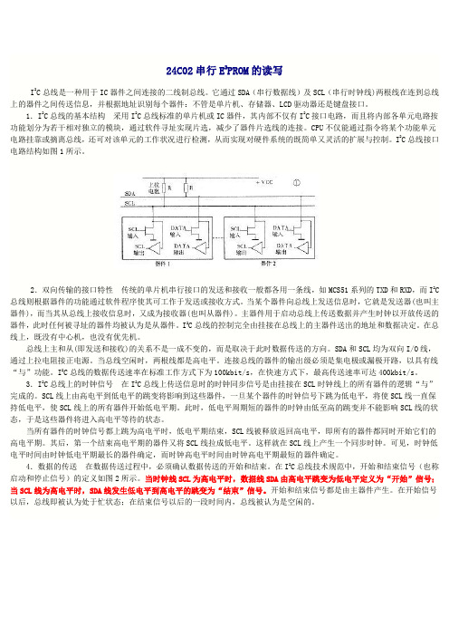
24C02串行E2PROM的读写I2C总线是一种用于IC器件之间连接的二线制总线。
它通过SDA(串行数据线)及SCL(串行时钟线)两根线在连到总线上的器件之间传送信息,并根据地址识别每个器件:不管是单片机、存储器、LCD驱动器还是键盘接口。
1.I2C总线的基本结构采用I2C总线标准的单片机或IC器件,其内部不仅有I2C接口电路,而且将内部各单元电路按功能划分为若干相对独立的模块,通过软件寻址实现片选,减少了器件片选线的连接。
CPU不仅能通过指令将某个功能单元电路挂靠或摘离总线,还可对该单元的工作状况进行检测,从而实现对硬件系统的既简单又灵活的扩展与控制。
I2C总线接口电路结构如图1所示。
2.双向传输的接口特性传统的单片机串行接口的发送和接收一般都各用一条线,如MCS51系列的TXD和RXD,而I2C 总线则根据器件的功能通过软件程序使其可工作于发送或接收方式。
当某个器件向总线上发送信息时,它就是发送器(也叫主器件),而当其从总线上接收信息时,又成为接收器(也叫从器件)。
主器件用于启动总线上传送数据并产生时钟以开放传送的器件,此时任何被寻址的器件均被认为是从器件。
I2C总线的控制完全由挂接在总线上的主器件送出的地址和数据决定。
在总线上,既没有中心机,也没有优先机。
总线上主和从(即发送和接收)的关系不是一成不变的,而是取决于此时数据传送的方向。
SDA和SCL均为双向I/O线,通过上拉电阻接正电源。
当总线空闲时,两根线都是高电平。
连接总线的器件的输出级必须是集电极或漏极开路,以具有线“与”功能。
I2C总线的数据传送速率在标准工作方式下为100kbit/s,在快速方式下,最高传送速率可达400kbit/s。
3.I2C总线上的时钟信号在I2C总线上传送信息时的时钟同步信号是由挂接在SCL时钟线上的所有器件的逻辑“与”完成的。
SCL线上由高电平到低电平的跳变将影响到这些器件,一旦某个器件的时钟信号下跳为低电平,将使SCL线一直保持低电平,使SCL线上的所有器件开始低电平期。
常用存储器的代换对照存储器, 代换PCA8581=24C01PCA8582=24C02PCE8522EP=24C02PCF8594C-2=24C04PCF8598C=24C08A510C=24C08(直接代换)代换时注意第7脚的状态,一般24C系列7脚都是接地的。
存储器24C04在彩电中运用广泛,目前大多数品牌彩电均选用它的系列型号作为存储器,其系列型号为:24C0l、24C02、24C04、24C08、24C16、24C32等等。
根据不同的制造厂商,在它们的前面冠以不同的字母,如AT、ST、BR、SL、KOR、KS等。
它们之间代换时,重点对⑦脚进行改接。
存储器24C04引脚功能与参数见表7。
存储器24C04的特点:(1)存储容量大,有4000bit,可存储100套电视节目(注:24C02存储60套,24C08存储200套);(2)外围电路简洁,内部设计有I2C接口电路,很方便地通过数据线与CPU连接,实现I2C总线控制,提高整机的工作性能;(3)工作电压范围宽2.5~6.8V,当电压为6V时写入峰值电流为3mA,最大读取电流150μP,待机时电流1μA左右,典型工作电压为5V左右;(4)内部设计有数据写入保护电路;(5)断电后内部数据可保存80年以上;(6)有噪音抑制功能,采用施密特触发器。
更换存储器24C04应注意:1.长虹2918FN彩电中,24C04典型连接图如图6所示。
图62.当微处理器及外围电路正常后需要更换存储器,只能用尾数大于或等于的型号代换,否则会造成存储节目数量减少,有的会造成某些功能失常等。
3.更换24C04系列存储器时,必须注意该存储器的制造商及电路板上⑦脚的接法。
24CXX系列存储器⑦脚的功能有:写保护控制(Wt))、取消写保护控制。
当⑦脚为低电平时,即⑦脚接地.为取消写保护控制。
这时微处理器通过总线写入需要存储的数据.完成存储,制造商有AT、ST、BR等生产的24CXX系列存储器:当⑦脚为高电平时,即⑦脚通过一只10kΩ上拉电阻至5V电眍,处于写保护状态,如果是.AT、ST、BR等厂商的24CXX系列存储器不能存入数据,KOR、KS等韩国厂商的24CXX系列存储器却能写入数据存储。
S P E C I F I C A T I O N24C02/24C04/24C08/24C16Version 1.0Two-wire Serial EEPROM2K bits (256 X 8) / 4K bits (512 X 8) / 8K bits (1024 X 8) / 16K bits (2048 X 8)▉FeaturesThe 24C02/24C04/24C08/24C16 provides 2048/4096/8192/16384 bits of serial electrically erasable and programmable read-only memory (EEPROM) organized as 256/512/1024/2048 words of 8 bits each. The device is optimized for use in many industrial and commercial applications wherelow-power and low-voltage operation are essential. The 24C02/24C04/24C08/24C16 is available in space-saving 8-lead PDIP, 8-lead SOP, and 8-lead TSSOP packages and is accessed via a two-wire serial interface.▉Pin ConfigurationTwo-wire Serial EEPROM2K bits (256 X 8) / 4K bits (512 X 8) / 8K bits (1024 X 8) / 16K bits (2048 X 8)▉Pin DescriptionsTwo-wire Serial EEPROM2K bits (256 X 8) / 4K bits (512 X 8) / 8K bits (1024 X 8) / 16K bits (2048 X 8)▉Pin Descriptions24C02, 2K SERIAL EEPROM: Internally organized with 32 pages of 8 bytes each, the 2K requires an 8-bit data word address for random word addressing.24C04, 4K SERIAL EEPROM: Internally organized with 32 pages of 16 bytes each, the 4K requires a 9-bit data word address for random word addressing.24C08, 8K SERIAL EEPROM: Internally organized with 64 pages of 16 bytes each, the 8K requires a 10-bit data word address for random word addressing.24C16, 16K SERIAL EEPROM: Internally organized with 128 pages of 16 bytes each, the 16K requires an 11-bit data word address for random word addressing.▉Device OperationTwo-wire Serial EEPROM 2K bits (256 X 8) / 4K bits (512 X 8) / 8K bits (1024 X 8) / 16K bits (2048 X 8)Two-wire Serial EEPROM2K bits (256 X 8) / 4K bits (512 X 8) / 8K bits (1024 X 8) / 16K bits (2048 X 8) The 2K, 4K, 8K and 16K EEPROM devices all require an 8-bit device address word following a start condition to enable the chip for a read or write operation (see to Figure 4 on page 7).The device address word consists of a mandatory "1", "0" sequence for the first four most significant bits as shown. This is common to all the Serial EEPROM devices.The next 3 bits are the A2, A1 and A0 device address bits for the 2K EEPROM. These 3 bits must compare to their corresponding hardwired input pins.The 4K EEPROM only uses the A2 and A1 device address bits with the third bit being a memory page address bit. The two device address bits must compare to their corresponding hardwired input pins. The A0 pin is no connect.The 8K EEPROM only uses the A2 device address bit with the next 2 bits being for memory page addressing. The A2 bit must compare to its corresponding hard-wired input pin. The A1 and A0 pins are no connect.The 16K does not use any device address bits but instead the 3 bits are used for memory page addressing. These page addressing bits on the 4K, 8K and 16K devices should be considered the most significant bits of the data word address which follows. The A0, A1 and A2 pins are no connect.The eighth bit of the device address is the read/write operation select bit. A read operation is initiated if this bit is high and a write operation is initiated if this bit is low.Upon a compare of the device address, the EEPROM will output a "0". If a compare is not made, the chip will return to a standby state.▉Write OperationsTwo-wire Serial EEPROM2K bits (256 X 8) / 4K bits (512 X 8) / 8K bits (1024 X 8) / 16K bits (2048 X 8) Read operations are initiated the same way as write operations with the exception that the read/write select bit in the device address word is set to "1". There are three read operations: current address read,random address read and sequential read.CURRENT ADDRESS READ: The internal data word address counter maintains the last address accessed during the last read or write operation, incremented by one. This address stays valid between operations as long as the chip power is maintained. The address "roll over" during read is from the last byte of the last memory page to the first byte of the first page. The address "roll over" during write is from the last byte of the current page to the first byte of the same page.Once the device address with the read/write select bit set to "1" is clocked in and acknowledged by the EEPROM, the current address data word is serially clocked out. The microcontroller does not respond with an input "0" but does generate a following stop condition (see Figure 7 on page 8).RANDOM READ: A random read requires a "dummy" byte write sequence to load in the data word address. Once the device address word and data word address are clocked in and acknowledged by the EEPROM, the microcontroller must generate another start condition. The microcontroller now initiates a current address read by sending a device address with the read/write select bit high. The EEPROM acknowledges the device address and serially clocks out the data word. The microcontroller does not respond with a "0" but does generate a following stop condition (see Figure 8 on page 8). SEQUENTIAL READ: Sequential reads are initiated by either a current address read or a randomTwo-wire Serial EEPROM 2K bits (256 X 8) / 4K bits (512 X 8) / 8K bits (1024 X 8) / 16K bits (2048 X 8)Two-wire Serial EEPROM2K bits (256 X 8) / 4K bits (512 X 8) / 8K bits (1024 X 8) / 16K bits (2048 X 8)l Absolute Maximum Stress RatingsDC Supply Voltage . . . . . . . . . . . . . . . . .-0.3V to +6.5V Input / Output Voltage . . . . . . . .GND-0.3V to V CC+0.3V Operating Ambient Temperature . . . . . -40℃to +85℃Storage Temperature . . . . . . . . . . . . -65℃to +150℃l CommentsStresses above those listed under "Absolute Maximum Ratings" may cause permanent damage to this device. These are stress ratings only. Functional operation of this device at these or any other conditions above those indicated in the operational sections of this specification is not implied or intended. Exposure to the absolute maximum rating conditions for extended periods may affect device reliability.Two-wire Serial EEPROM2K bits (256 X 8) / 4K bits (512 X 8) / 8K bits (1024 X 8) / 16K bits (2048 X 8)▉DC Electrical CharacteristicsApplicable over recommended operating range from TA = 25 ℃, f = 1.0 MHz, VCC = +1.8V Parameter Symbol Min. Typ. Max. Unit ConditionCI/O - - 8 pF VI/O = 0V Input/Output Capacitance(SDA)Input Capacitance (A0, A1,CIN - - 8 pF VIN = 0V A2, SCL)▉AC Electrical CharacteristicsTwo-wire Serial EEPROM2K bits (256 X 8) / 4K bits (512 X 8) / 8K bits (1024 X 8) / 16K bits (2048 X 8) Figure 10: SCL: Serial Clock, SDA: Serial Data I/OTwo-wire Serial EEPROM2K bits (256 X 8) / 4K bits (512 X 8) / 8K bits (1024 X 8) / 16K bits (2048 X 8)▉Write Cycle Timing。