新编单片机第4章80C51的汇编语言程序的设计精选文档PPT课件
- 格式:ppt
- 大小:2.77 MB
- 文档页数:17

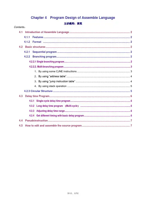
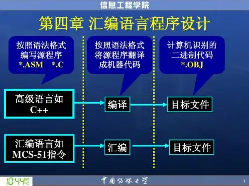
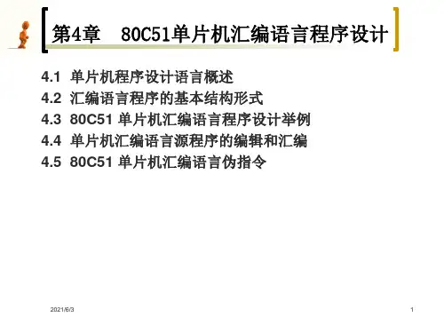
Chapter 4 Program Design of Assemble Language主讲教师:黄英Contents:4.1 Introduction of Assemble Language (2)4.1.1 Features (2)4.1.2 Format (2)4.2 Basic structures (2)4.2.1 Sequential program (2)4.2.2 Branching program (2)4.2.2.1 Single branching program (2)4.2.2.2. Multi-branching program (3)1.By using some CJNE instructions (3)2.By using “address table” (4)3.By using “jump instruction table” (4)4.By using stack operation (5)4.2.3 Circular Structure (5)4.3 Delay time Program (6)4.3.1 Single-cycle delay time program (6)4.3.2 Long delay time program (Multi-cycle) (6)4.3.3 Adjusting delay time range (6)4.3.4 Get different timing with basic delay program (6)4.4 Pseudoinstruction (7)4.5 How to edit and assemble the source program (7)4.1 Introduction of Assemble Language4.1.1 Features1. P roduces the optimized program.2. P rogrammer must be familiar with hardware. 3. M anage and control hardware directly . 4. N ot universal, can ’t be transplanted.4.1.2 Format (Detailed information: P77)[<Label>]: <opcode> [<operand>]; [<note>]4.2 Basic structures3 types:✧ Sequential Structure ✧ Branching Structure ✧ Circular Structure4.2.1 Sequential programFor example: 3-byte unsigned constants addition4.2.2 Branching program4.2.2.1 Single branching program·Using jump instructions :P67-68: JZ, JNZ, CJNE, DJNZ (条件转移指令) P73-74: JC, JNC, JB, JNB, JBC (位控制转移指令)Assumed that: 50H~52H cells of internal RAM have three augends respectively (beginning with high bytes ), 53H~55H cells of internal RAM have three addends respectively (beginning with high bytes ).Requirement: Design a program to put the additionresult into 50H~52H cells (beginning with high bytes ), and the carry bit into 20H bit of bit addressable area .MOV R0, #52H MOV R1, #55H ① MOV A, @R0ADD A, @R1 MOV @R0, A DEC R0 DEC R1② MOV A, @R0 ADDC A, @R1MOV @R0, ADECR0 (50H/51H/52H )= 11H/22H/33H DEC R1 (53H/54H/55H )= 77H/88H/99H ③ MOV A, @R0ADDC A, @R1 112233H MOV @R0, A + 778899H CLR AADDC A, #00H ? ④ MOV R0, #20H ?MOV @R0, A ?For example: Compare the valuesSTAR T: CLR C; clear the carry bitMOV DPTR, #ST1 ; set the data pointer MOV X A, @DPTRMOV R2, A ; put the 1stconstant into R2INC DPTR MOV X A, @DPTR ; put the 2st constant into ASUBB A, R2 ; A = A – R2= 2st - 1stJNC BIG1 ; if no carry, then the 2st constant is bigger . XCH A, R2 ; else 1st constant is bigger , and put into A BIG0: INC DPTR ; let DPTR points to the result cell. MOVX @DPTR, A ; save the bigger constant. RETBIG1: MOV X A, @DPTR ; put the 2st constant into ASJMP BIG04.2.2.2. Multi-branching program· Instruction Set has no multi-branching instruction. · 4 methods to realize multi-branching:1.By using some CJNE instructions 2.By using “address table ”3.By using “jump instruction table ” 4.By using stack operation1.By using some CJNE instructionsCJNEA, #data, rel ; put the branching number into A.For example: temperature control systemCJNE A, 55H, LOOP1 ; if T a ≠T55(upper value limit ),then j ump to LOOP1 AJMP FH ; T a =T55,j ump to main program FH (返回) LOOP1: JNC JW ; if CY ≠0,T a >T55, then j ump to JW (降温)CJNE A, 54H, LOOP2 ; if T a ≠T54(low er value limit ),then j ump to LOOP2 AJMP FH ; T a =T54,j ump to main program (FH ) LOOP2: JC SW ; if CY =1,T a <T54, then j ump to SW (升温)FH: RETAssumed that: There are three continuous cells (ST1, ST2, ST3)in the externalRAM where ST1 and ST2 have 8-bit unsigned binary constants respectively .Requirement: Design a program to find the bigger constant , and put it into ST3 cell.Assumed that: There is a temperature control system, which current temperature value (Ta ) is saved in A . The lower value limit (T54)of temperature control is saved in the internal RAM cell 54H , The upper value limit (T55)of temperature control is saved in the internal RAM cell 55H .Requirement: Design a program to control temperature under the conditions: If Ta > T55, then executes the temperature-down processing subprogram (JW ); If Ta < T54, then executes the temperature-up processing subprogram (SW ); If T55≥Ta ≥T54, then returns to the main program (FH ).2.By using “offset address table ”Step:(1)Set up a “offset address table ”(2)Using instruction: JMP @A+DPTRwhere: Offset table base address → DPTR Offset → A (offset value =BR0/BR1/BR2/BR3 - BRTAB )R3: 00, 01, 02, 03 MOV A, R3 ; put the branching number into AMOV DPTR, # BRT AB ; let DPTR point to base address of offset table MOVC A, @A+DPTR ; fetch the offset v alue.JMP @A+DPTR ; j ump to the corresponding subroutine. (A is offset value, DPTR is the address of BRT AB ); PC = A+DPTR BRT AB: DBBR0_BRTAB ; offset value of BR0 DB BR1_BRTAB ; offset value of BR1 DB BR2_BRTAB ; offset value of BR2 DBBR3_BRTAB; offset value of BR3BR0: MOV A, @R0 ; 00 ; fetch data from internal RAM to A (R0 saves low 8-bit address ) SJMP DONE ; stopBR1: MOV X A, @R0; 01; fetch data from ext ernal RA M (low er 256B )to A (R0 saves low 8-bit address ) SJMP DONE; stopBR2: MOV A, R1; 02; put high address into A < 4K = 212 = 24·28 > (R1 saves high 8-bit address ) ANL A, #0FH ; fetch low 4-bit from high address, and clear high 4-bit. ANL P2, #0F0H ; fetch high 4-bit from P2 port, and clear low 4-bit of P2 ORL P2, A ; not change high 4-bit of P2, and send low 4-bit of P2MOV X A, @R0 ; fetch data from external RAM (4KB )to A (R0 sav es low 8-bit address )SJMP DONE; stopBR3: MOV DPL, R0; 03; put low 8-bit address of ext ernal RA M to DPL MOV DPH, R1 ; put high 8-bit address of external RAM to DPHMOV X A, @DPTR; fetch data from external RAM (64KB )to A DONE : SJMP $; stop3.By using “jump instruction table ” For example:R3: 00, 01, 02, 03, … MOV A, R3 ; put the branching number into A RL A ; A = branching number × 2 MOV DPTR, # BRT AB ; let DPTR point to base address of offset table JMP @A+DPTR ; j ump to the corresponding subroutine, PC = A+DPTR BRT AB: AJMP ROUT0 ; j ump to ROUT0 AJMP ROUT1 ; j ump to ROUT1 AJMP ROUT2 ; j ump to ROUT2AJMP ROUT3 ; j ump to ROUT3 … AJMP ROUTn ; j ump to ROUTnWhy “RL A ” ?When R3 = 00, need j ump to BRT AB + 0, so A = 00, When R3 = 01, need j ump to BRT AB + 2, so A = 02, When R3 = 02, need j ump to BRT AB + 4, so A = 04, When R3 = 03, need j ump to BRT AB + 6, so A = 06.Assumed that: R3 saves branching number. BRTAB denotes the base address of jump instruction table.Requirement: Design a program to realize multi-branching. Offset table (offset value=BR0/BR1/BR2/BR3 - BRTAB )Jump instruction table4.By using stack operationSteps: (1)Put the 16-bit address into stack(2)Using RET instruction to get PC value from stack For example:·R3: 00, 01, 02, 03 MOV DPTR, # BRT AB ; let DPTR point to base address of offset table MOV A, R3 ; put the branching number into A RL A ; A = branching number × 2 MOV R1, A ; R1 = 2·R3 INC A ; A = 2·R 3 + 1 MOVC A , @A +DPTR ; fetch low 8-bit address to A PUSH ACC ; and put low 8-bit address into Stack. MOV A, R 1 MOVC A , @A +DPTR ; fetch high 8-bit address to A PUSH ACC ; and put it into Stack. RET ; set PC value from stack. Get high 8-bit address first, and then low 8-bit address . BRT AB: DW BR0 ; 16-bit address of branching subroutine 0DW BR1 ; 16-bit address of branching subroutine 1 DW BR2 ; 16-bit address of branching subroutine 2 DW BR3 ; 16-bit address of branching subroutine 3 …DW BRn ; 16-bit address of branching subroutine n4.2.3 Circular StructureMethod: Using conditional jump instructions.For example:MOV R2, #0FFH ; set the initial value of the length counter. MOV R0, #3FH ; set the initial value of the string pointer. LOOP: INC R2 ; R2 = 00H, 01H,… INC R0 ; R0 = 40H, 41H,…CJNE @R0, #0DH , LOOPRETAssumed that: R3 saves branching number .BRTAB denotes the base address of jump instruction table.Requirement: Design a program to realize multi-branching.Assumed that: There is a character string that adopts “Enter ” symbol as the ending flag. This string is saved in the internal RAM beginning with 40H cell. Requirement: Design a program to get the length of this string.16-bit address t able. Pay attention to the operation of DW!4.3 Delay time Program4.3.1 Single-cycle delay time programMOV R5, #TIME; 1LOOP: NOP ; 1 NOP ; 1 DJNZ R5, LOOP ; 2If f osc = 6MHz, then machine cycle T M :So total delay time: T max =1+(1+1+2)×2us ×TIME; TIME = 00H-FFH, 0-255, cycles 265 times=1+(1+1+2)×2us ×256 = 1+2048 = 2049us4.3.2 Long delay time program (Multi-cycle )MOVR5, #TIME1 ; 1LOOP2:MOV R4, #TIME2 ; 1 LOOP1:NOP; 1 NOP ; 1 DJNZ R4, LOOP1 ; 2 DJNZ R5, LOOP2 ; 2 RET; 2If f osc = 6MHz, then total delay time T max : T max = 1+((1+(1+1+2)×256+2)×256)+ 2 )× 2us = 1+ 525828 = 525829us4.3.3 Adjusting delay time range·by adding or deleting instructions that don ’t affect program function.MOV R0, #TIME1LOOP:ADD A, R1 ; 1 INC DPTR; 2DJNZ R0, LOOP; 2If f osc = 6MHz, then the delay time T of the cycle body is as follow :T = (1+2+2)×2us ×TIME = 10×TIME (us ) MOV R0, #TIME1LOOP: ADD A, R1 ; 1 INC DPTR ; 2 NOP; 1DJNZ R0, LOOP; 2If f osc = 6MHz, then the delay time T of the cycle body is as follow :T = (1+2+1+2)×2us ×TIME = 12×TIME (us )4.3.4 Get different timing with basic delay programMOV R0, #05H; 5s delay time LOOP1:LCALL DELA Y; 1s delay time DJNZ R0, LOOP1MOV R0, #0A H; 10s delay time LOOP2:LCALL DELA Y; 1s delay time DJNZ R0, LOOP2MOV R0, #14H; 20s delay time LOOP3:LCALL DELA Y ; 1s delay time DJNZ R0, LOOP32us126MHz1T M =⨯=4.4 Pseudoinstruction7 pseudoinstructions:ORG, END, EQU, DB, DW, DS, BIT(Read P93)Note: DB, DW, and DS are only used for program memory.4.5 How to edit and assemble the source program·hand assemble·Machine edit: get source program: *. asm·Across assembleHome Work of Chapter 4P98 (一)1、4 (二)6。