STM32F0-DISCOVERY用户手册
- 格式:pdf
- 大小:3.23 MB
- 文档页数:30
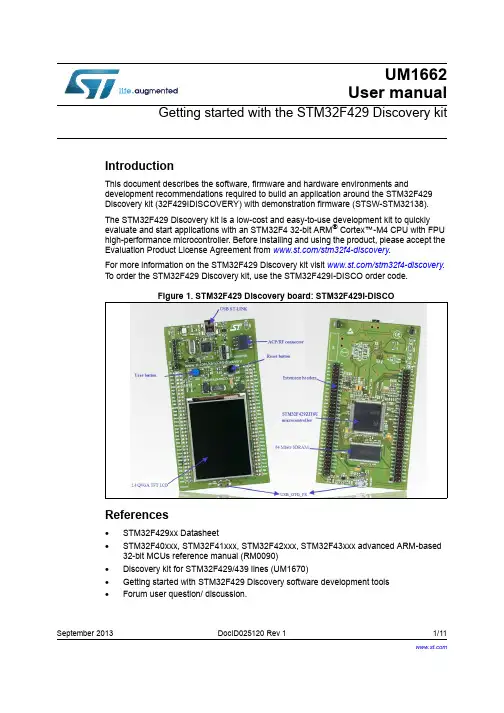
September 2013DocID025120 Rev 11/11UM1662User manualGetting started with the STM32F429 Discovery kitIntroductionThis document describes the software, firmware and hardware environments anddevelopment recommendations required to build an application around the STM32F429 Discovery kit (32F429IDISCOVERY) with demonstration firmware (STSW-STM32138).The STM32F429 Discovery kit is a low-cost and easy-to-use development kit to quickly evaluate and start applications with an STM32F4 32-bit ARM ® Cortex™-M4 CPU with FPU high-performance microcontroller. Before installing and using the product, please accept the Evaluation Product License Agreement from /stm32f4-discovery .For more information on the STM32F429 Discovery kit visit /stm32f4-discovery . To order the STM32F429 Discovery kit, use the STM32F429I-DISCO order code.Figure 1. STM32F429 Discovery board: STM32F429I-DISCOReferences•STM32F429xx Datasheet•STM32F40xxx, STM32F41xxx, STM32F42xxx, STM32F43xxx advanced ARM-based 32-bit MCUs reference manual (RM0090)•Discovery kit for STM32F429/439 lines (UM1670)•Getting started with STM32F429 Discovery software development tools •Forum user question/ discussion.Contents UM1662Contents1Hardware configuration and layout . . . . . . . . . . . . . . . . . . . . . . . . . . . . . 41.1Features . . . . . . . . . . . . . . . . . . . . . . . . . . . . . . . . . . . . . . . . . . . . . . . . . . . 41.2Microcontroller . . . . . . . . . . . . . . . . . . . . . . . . . . . . . . . . . . . . . . . . . . . . . . 41.3System requirement . . . . . . . . . . . . . . . . . . . . . . . . . . . . . . . . . . . . . . . . . . 51.4Powering up the board . . . . . . . . . . . . . . . . . . . . . . . . . . . . . . . . . . . . . . . . 51.5Reset the board . . . . . . . . . . . . . . . . . . . . . . . . . . . . . . . . . . . . . . . . . . . . . 61.6Hardware block diagram . . . . . . . . . . . . . . . . . . . . . . . . . . . . . . . . . . . . . . 62Firmware package . . . . . . . . . . . . . . . . . . . . . . . . . . . . . . . . . . . . . . . . . . . 72.1Package description . . . . . . . . . . . . . . . . . . . . . . . . . . . . . . . . . . . . . . . . . . 72.2Programming firmware application . . . . . . . . . . . . . . . . . . . . . . . . . . . . . . . 72.2.1Programming application . . . . . . . . . . . . . . . . . . . . . . . . . . . . . . . . . . . . . 82.2.2Run pre-loaded demo . . . . . . . . . . . . . . . . . . . . . . . . . . . . . . . . . . . . . . . 8 3Revision history . . . . . . . . . . . . . . . . . . . . . . . . . . . . . . . . . . . . . . . . . . . 102/11DocID025120 Rev 1UM1662List of figures List of figuresFigure 1.STM32F429 Discovery board: STM32F429I-DISCO . . . . . . . . . . . . . . . . . . . . . . . . . . . . . . 1 Figure 2.STM32F429I-DISCO power sources . . . . . . . . . . . . . . . . . . . . . . . . . . . . . . . . . . . . . . . . . . 7 Figure 3.Hardware block diagram. . . . . . . . . . . . . . . . . . . . . . . . . . . . . . . . . . . . . . . . . . . . . . . . . . . . 8 Figure 4.Package contents. . . . . . . . . . . . . . . . . . . . . . . . . . . . . . . . . . . . . . . . . . . . . . . . . . . . . . . . . 9 Figure 5.Hardware environnement. . . . . . . . . . . . . . . . . . . . . . . . . . . . . . . . . . . . . . . . . . . . . . . . . . 11DocID025120 Rev 13/111 Hardware configuration and layout1.1 FeaturesThe STM32F429 Discovery offers the following features:•STM32F429ZIT6 microcontroller featuring 2 MB of Flash memory, 256 KB of RAM in an LQFP144 package•On-board ST-LINK/V2 with selection mode switch to use the kit as a standalone ST-LINK/V2 (with SWD connector for programming and debugging)•Board power supply: through the USB bus or from an external 3 V or 5 V supply voltage•L3GD20, ST MEMS motion sensor, 3-axis digital output gyroscope•TFT LCD (Thin-film-transistor liquid-crystal display) 2.4", 262K colors RGB,240x320dots•SDRAM 64 Mbits (1Mbit x 16-bit x 4-bank) including an AUTO REFRESH MODE, anda power-saving•Six LEDs:–LD1 (red/green) for USB communication–LD2 (red) for 3.3 V power-on–Two user LEDs:LD3 (green), LD4 (red)–Two USB OTG LEDs:LD5 (green) VBUS and LD6 (red) OC (over-current)•Two pushbuttons (user and reset)•USB OTG with micro-AB connector•Extension header for LQFP144 I/Os for a quick connection to the prototyping board and an easy probing1.2 MicrocontrollerThe STM32F429ZIT6U device is based on the high-performance ARM® Cortex™-M4 32-bitRISC core operating at a frequency of up to 180 MHz The Cortex-M4 core features aFloating point unit (FPU) single precision which supports all ARM single-precisiondata-processing instructions and data types. It also implements a full set of DSP instructionsand a memory protection unit (MPU) which enhances application security.The STM32F429ZIT6U device incorporates high-speed embedded memories (2Mbytes ofFlash memory, 256 Kbytes of SRAM), up to 4 Kbytes of backup SRAM, and an extensiverange of enhanced I/Os and peripherals connected to two APB buses, two AHB buses anda 32-bit multi-AHB bus matrix.4/11DocID025120 Rev 1DocID025120 Rev 15/111.3 System requirement•Windows PC (XP , Vista, 7)•USB type A to Mini-B USB cable •ST-LINK/V2•Supported IDE are EWARM (IAR Embedded Workbench ®), MDK-ARM™ and AtollicTrueSTUDIO ®Note:Required information to download and install desired IDE and ST-LINK/V2 are detailed in Getting started with STM32F429 Discovery software development tools document.1.4 Powering up the boardThe STM32F429I-DISCO board can be powered up from three sources.•USB ST-LINK: To power the board from the USB connector CN1, use the 'USB type Ato Mini-B' cable and connect it between the host and the board USB connector CN1. •External sources: DC power supply can be inserted in the GND and 3V (or 5V) pin.Figure 2. STM32F429I-DISCO power sourcesUSB ST-LINK (CN1)5V 3V1.5 Reset the boardThere are three ways to reset the board:•Push the reset button mounted on the STM32F429I-DISCO.•Remove and reinsert the USB cable.•The MCU can also be reset by debuggers.1.6 Hardware block diagramThe STM32F429I-DISCO is designed around the STM32F429ZIT6U microcontroller in a144-pin LQFP package. Figure3 illustrates the connections between the STM32F429ZIT6Uand its peripherals (STLINK/V2, pushbutton, LED, USB and connectors).Please refer to schematic under /stm32f4-discovery for more details.6/11DocID025120 Rev 1DocID025120 Rev 17/11UM1662Firmware package2 Firmware packageTo get started with the STM32F429 Discovery kit, a firmware package that contains a set ofIP examples and demonstrations of some features exists under /stm32f4-discovery .2.1 Package descriptionThe STM32F429 Discovery firmware applications, demonstration and IPs examples areprovided in one single package and supplied in one single zip file. The extraction of the zip file generates one folder, STM32F429I-Discovery_FW_VX.Y.Z , which contains the following subfolders:Figure 4. Package contentsUser can run examples provided within this package. A set of examples for each peripheral are ready to be run.2.2 Programming firmware applicationTo start programming, user must:•Install preferred Integrated Development Environment (IDE)•Install the ST-LINK V2 driver from ST web siteFirmware package UM16628/11DocID025120 Rev 12.2.1 Programming applicationTo program application (demonstration or example), follow the sequence below:1.Go under application folder 2. Chose the desired IDE project3. Double click on the project file (ex. STM32F429I-Discovery_Demo.eww for EWARM)4. Rebuild all files: Project->Rebuild all5.Load project image: Project->Debug6. Run program: Debug->GoPlease refer to Getting started with STM32F429 Discovery software development toolsfor more details.2.2.2 Run pre-loaded demoTo run and develop any firmware applications on your STM32F429 Discovery board, theminimum requirements are as follows:–Windows PC (XP , Vista, 7)–‘USB type A to Mini-B' cable, used to power the board (through USB connector CN1) from host PC and connect to the embedded ST-LINK/V2 for debugging and Programming.Additional hardware accessories will be needed to run some applications:–‘USB type A to Micro-B' cable, used to connect the board (through USB connector CN5) as USB Device to host PC.DocID025120 Rev 19/11UM1662Firmware packageEstablish the connection with the STM32F429 Discovery board as follows:Figure 5. Hardware environnementThe demonstration software, based on the STemWin GUI library, is already preloaded in the board's Flash memory. It uses the LCD TFT mounted on the board to show the Menu based-on-icon view widget (Image Browser, Game, Performance, Clock/Calendar, Video and System Info module). The status bar indicate the CPU Usage, date, USB disk flash connection state, alarm and time.Follow the sequence below to configure the STM32F429 Discovery board and launch the DISCOVER application:1.Ensure that the jumpers JP3 and CN4 are set to "on" (Discovery mode).2.Connect the STM32F429 Discovery board to a PC using a USB cable type A/mini-B through the USB ST-LINK connector CN1, to power the board. The LEDs LD2 (PWR) and LD1 (COM).3.The following applications are available on the screen:–Clock/Calendar and Game–Video Player and Image Browser (play videos and view images from the USB mass storage connected to CN6)–Performance monitor (watch the CPU load and run a graphical benchmark)–System Info4. The demo software, as well as other software examples that allow you to discover the STM32 F4 series features, are available on /stm32f4-discovery .5.Develop your own applications starting from the examples.Revision history UM166210/11DocID025120 Rev 13 Revision historyTable 1. Document revision historyDate Revision Changes09-Sep-20131Initial release.UM1662Please Read Carefully:Information in this document is provided solely in connection with ST products. STMicroelectronics NV and its subsidiaries (“ST”) reserve the right to make changes, corrections, modifications or improvements, to this document, and the products and services described herein at any time, without notice.All ST products are sold pursuant to ST’s terms and conditions of sale.Purchasers are solely responsible for the choice, selection and use of the ST products and services described herein, and ST assumes no liability whatsoever relating to the choice, selection or use of the ST products and services described herein.No license, express or implied, by estoppel or otherwise, to any intellectual property rights is granted under this document. If any part of this document refers to any third party products or services it shall not be deemed a license grant by ST for the use of such third party products or services, or any intellectual property contained therein or considered as a warranty covering the use in any manner whatsoever of such third party products or services or any intellectual property contained therein.UNLESS OTHERWISE SET FORTH IN ST’S TERMS AND CONDITIONS OF SALE ST DISCLAIMS ANY EXPRESS OR IMPLIED WARRANTY WITH RESPECT TO THE USE AND/OR SALE OF ST PRODUCTS INCLUDING WITHOUT LIMITATION IMPLIED WARRANTIES OF MERCHANTABILITY, FITNESS FOR A PARTICULAR PURPOSE (AND THEIR EQUIVALENTS UNDER THE LAWS OF ANY JURISDICTION), OR INFRINGEMENT OF ANY PATENT, COPYRIGHT OR OTHER INTELLECTUAL PROPERTY RIGHT.ST PRODUCTS ARE NOT DESIGNED OR AUTHORIZED FOR USE IN: (A) SAFETY CRITICAL APPLICATIONS SUCH AS LIFE SUPPORTING, ACTIVE IMPLANTED DEVICES OR SYSTEMS WITH PRODUCT FUNCTIONAL SAFETY REQUIREMENTS; (B) AERONAUTIC APPLICATIONS; (C) AUTOMOTIVE APPLICATIONS OR ENVIRONMENTS, AND/OR (D) AEROSPACE APPLICATIONS OR ENVIRONMENTS. WHERE ST PRODUCTS ARE NOT DESIGNED FOR SUCH USE, THE PURCHASER SHALL USE PRODUCTS AT PURCHASER’S SOLE RISK, EVEN IF ST HAS BEEN INFORMED IN WRITING OF SUCH USAGE, UNLESS A PRODUCT IS EXPRESSLY DESIGNATED BY ST AS BEING INTENDED FOR “AUTOMOTIVE, AUTOMOTIVE SAFETY OR MEDICAL” INDUSTRY DOMAINS ACCORDING TO ST PRODUCT DESIGN SPECIFICATIONS. PRODUCTS FORMALLY ESCC, QML OR JAN QUALIFIED ARE DEEMED SUITABLE FOR USE IN AEROSPACE BY THE CORRESPONDING GOVERNMENTAL AGENCY.Resale of ST products with provisions different from the statements and/or technical features set forth in this document shall immediately void any warranty granted by ST for the ST product or service described herein and shall not create or extend in any manner whatsoever, any liability of ST.ST and the ST logo are trademarks or registered trademarks of ST in various countries.Information in this document supersedes and replaces all information previously supplied.The ST logo is a registered trademark of STMicroelectronics. All other names are the property of their respective owners.© 2013 STMicroelectronics - All rights reservedSTMicroelectronics group of companiesAustralia - Belgium - Brazil - Canada - China - Czech Republic - Finland - France - Germany - Hong Kong - India - Israel - Italy - Japan - Malaysia - Malta - Morocco - Philippines - Singapore - Spain - Sweden - Switzerland - United Kingdom - United States of AmericaDocID025120 Rev 111/11。
STM32F407 Discovery ExtBoard用户手册版本 2011-05-01(本手册不断更新,建议您在官方网站下载最新版本)版权声明本手册版权归属天津淘淘科技电子有限公司(以下简称“淘淘科技”)所有, 并保留一切权力。
非经淘淘科技同意(书面形式),任何单位及个人不得擅自摘录本手册部分或全部,违者我们将追究其法律责任。
敬告:在售开发板的手册会经常更新,请在 网站查看最近更新,并下载最新手册,恕不再另行通知。
更新说明日期说明2012-05-01 本手册第一次发布目录1.1 STM32F407 Discovery ExtBoard开发板简介STM32F407 Discovery ExtBoard(下简称“本开发板”)是一款十分精致的低价高品质一体化STM32F407 Discovery CortexM4扩展开发板,由天津淘淘科技设计、生产和发行销售。
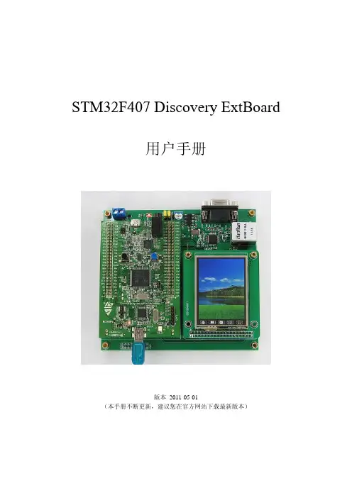
它采用STM32F407 Discovery作为核心板(下简称“核心板”),在设计上最大限度的贴近STM公司的开发板“精细”的风格,而且布局更加合理,接口更加丰富,十分适用于开发 MID、汽车电子、工业控制、导航系统、媒体播放等终端设备;也可适用于高校教学、嵌入式培训、个人研究学习和DIY 等。
具体而言,本开发板除了保留原有核心板的重力感应、三轴加速度传感器、miniUSB(A-B两种接口)、3.5mm 音频输出口、100PIN GPIO、LED、用户按键以外,本开发板还扩展了 LCD、4 线电阻触摸屏接口、100M 标准网络接口、DB9 串口、CAN总线接口、SD 卡接口、数字Camera接口,并为用户提供了AD 可调电阻等。
所有这些,都极大地方便了开发者的评估和使用,再加上我们按照本开发板尺寸专门定制的 LCD 模块,真正做到充分发挥STM官方原装开发板的强大功能。
我们还充分地发挥了原装开发板在线调试的ST-Link/v2,您不必再额外购买JTAG仿真器等调试设备,仅需要一根usb线就可以在尽情发挥CortexM4的特性。

STM32F103VET6芯达 STM32○RUser's ManualPreliminaryRevision 1.0(2010.06.08) 芯达STM32开发板开发指南Copyright © 2009‐2010 ARM79 Limited. All rights reserved版本信息本手册进行了以下更改。
芯达STM32用户手册修订记录日期 修订版本 CR ID 修改章节 修改描述 作者 2010-5-28 1.00 全部 创建 林辰 2010-8-16 1.10 去掉蜂鸣器、AT45 林辰 2010-8-20 1.20 增加外扩接口、修林辰改外观图片版权声明本手册版权归属(以下简称“arm79”)所有, 并保留一切权力。
非经arm79同意(书面形式),任何单位或个人不得擅自摘录本手册部分或全部,违者我们将追究其法律责任。
敬告:在售开发板的手册会经常更新,请在网站查看最近更新,并下载最新手册,不再另行通知。
目录目录 (4)写在前面 (5)第一章芯达STM32光盘使用说明 (6)第二章芯达STM32硬件说明 (8)2.1 芯达STM32板载资源说明 (8)2.2 芯达STM32原理图说明 (9)2.2.1电源电路 (9)2.2.2 实时时钟(备用电池)电路 (9)2.2.3 系统时钟电路 (9)2.2.4 JTAG接口电路 (10)2.2.5 复位电路 (10)2.2.6 用户LED电路 (10)2.2.7 串口电路 (11)2.2.8 按键电路 (11)2.2.9 SD卡接口电路 (12)2.2.10 USB接口电路 (12)2.2.11 LCD TFT液晶接口电路 (13)2.2.12 外扩IO接口电路 (13)第三章芯达STM32开发前的准备 (15)3.1 J-Link驱动的安装 (15)3.2 使用J-Link下载调试 (18)3.3使用ISP下载调试 (25)3.3.1 安装Flash loader (25)3.3.2 使用ISP下载调试 (28)3.4安装RealView MDK软件 (34)3.5使用MDK + J-Link调试 (38)第四章芯达STM32初步开发举例 (49)4.1 下载固件库 (49)4.2 STM32简单开发 (50)附福州芯达工作室简介 (54)写在前面感谢您选购芯达STM32开发板产品!请详细阅读以下文字,以获取对芯达STM32开发板的更多信息。
Open32F0-D User ManualContents1. Overview (2)1.1. What’s on board (2)2. Demo (4)2.1. 8IOs (4)2.2. 24L01 (5)2.3. ADC+DMA (5)2.4. DAC+DMA (6)2.5. FATFS V0.08A-SD Card (6)2.6. GPIO LED (7)2.7. GPIO LED JOYSTICK (7)2.8. I2C (7)2.9. I2S UDA1380 & SD_FatFS(DMA) (8)2.10. JOYSTICK (8)2.11. LCD22-picture (8)2.12. LCD22_TouchPanel (9)2.13. One-Wire (10)2.14. SPI (10)2.15. uCOS-II-V2.91 (11)2.16. uCOS-II-V2.91+LCD (11)2.17. USART (11)3. Revision history (12)1. Overview 1.1. What’s on board[ Core interface ]1. STM32F0DISCOVERY socketfor easily connecting theSTM32F0DISCOVERY2. 8I/Os + DAC + ADC interfacefor connecting accessory boards such buttons, motors, AD/DA module etc.3. USART2 interfaceeasily connects to RS232, RS485, USB TO232, etc.4. SPI1/SPI2 interface[ Other interface ]10. 5V/3.3V power input/outputusually used as power output, alsocommon-grounding with other user board11. 5V DC jack12. MCU pins connectorall the MCU I/O ports are accessible onexpansion connectors for further expansion 13. SWD interfacefor debugging/programmingeasily connects to SPI peripherals such asDataFlash (AT45DBxx), SD card, MP3 module, etc.5. LCD connectorfor connecting touch screen LCD 6.USART1 interfaceeasily connects to RS232, RS485, USB TO 232, etc.7.I2C1 / I2C2 interfaceeasily connects to I2C peripherals such as I/O expander (PCF8574), FRAM (FM24CLxx), etc. 8.I2S / I2C1 interfaceeasily connects to I2S peripherals such as audio module, etc. 9.1-WIRE interfaceeasily connects to ONE-WIRE devices (TO-92 package), such as temperature sensor (DS18B20), electronic registration number (DS2401), etc.[ Jumper/switch ] •Joystick jumpershort the jumper to connect the joystick to default I/Os used in example code;open the jumper to connect the joystick to custom I/Os via jumper wires14. Boot mode switchfor configuring BOOT0 pin.[ Component ] 15. Power switch 16. Power indicator17. Joystick: five positions2. DemoKEIL MDK Version :4.54Programmer/Debugger: STM32F0DISCOVERY onboard SWD Programming/Debugging interface: SWDSerial port settings:2.1. 8IOs◆ Overview8bit I/Os demo◆ Hardware connectionConnect the RS232 board to the onboardUSART1 interfaceConnect the 8 Push Button to the onboard 8I/Os connector (Make sure the G pinheader is connect to the board GND pinheader)◆ Operation and result◆The below information will be printed on the serial debugging assistantSelect a proper COM portBaud rate 115200Data bits 8Stop bits 1 Parity bitsNoneFlow control None2.2. 24L01◆ OverviewNRF24L01 demo ◆ Hardware connectionConnect the RS232 board to the onboardUSART1 interfaceConnect the two NRF24L01 to the board viaSPI interface ◆ Software configurationTwo NRF24L01 are needed for this demo, configuring as below:When configuring as sending mode, enable: #define T_O_R 1, comment out: //#define T_O_R 0 When configuring as receiving mode, enable: #define T_O_R 0, comment out: //#define T_O_R 0. ◆ Operation and resultMessage will be printed on the serial debugging assistant.2.3. ADC+DMA◆ OverviewADC+DMA demo◆ Hardware connectionConnect the RS232 board to the onboardUSART1 interfaceConnect the Analog Test Board to the board via8 I/Os (ADC+DAC)◆ Operation and resultRotate the onboard potentiometer, the AD message will be printed on the serial debugging assistant:2.4. DAC+DMA◆ OverviewDAC+DMA demo◆ Hardware connectionConnect the Analog Test Board to the board via8 I/Os (ADC+DAC)Connect the 5V pinheaders on both the mainboard and the Analog Test Board via jumper wire◆ Operation and resultYou may hear sound from the Analog Test Board when press the Reset button2.5. FATFS V0.08A-SD Card◆ OverviewSD_FatFS demo ◆ Hardware connectionConnect the RS232 board to the onboardUSART1 interfaceConnect the Micro SD Storage Board to theboard via SDIO interface.Insert the SD card to the Micro SD Storage Board socketConnect the CD pin on the Micro SD StorageBoard to the board PB0 pin via Dupont wire.`◆ Operation and resultThe below information will be printed on the serial debugging assistant:2.6. GPIO LED◆ OverviewLED demo◆ Hardware connection ◆ Operation and resultThe two LEDs on the Discovery board blinking2.7. GPIO LED JOYSTICK◆ OverviewUser key demo◆ Hardware connection ◆ Operation and resultPress the User key, the LED status will change accordingly.2.8. I2C◆ OverviewI2C EEPROM demo ◆ Hardware connectionConnect the RS232 board to the onboardUSART1 interfaceConnect the AT24/FM24 Board to theI2CX connector ( connect to I2C1 or I2C2 depends on the program)◆ Operation and resultThe below information will be printed on the serial debugging assistant:2.9. I2S UDA1380 & SD_FatFS(DMA)◆ OverviewAudio file placed on SD Card (with FATFS) ◆ Hardware connectionConnect Micro SD Storage Board to the board viaSPI2 interface.Insert the SD card to the Micro SD Storage Boardsocket. Connect the CD pin of the Micro SD Storage Boardto the board PB0 pin via DuPont wire. Put “audio.wav“ file to the SD cardConnect UDA1380 Board to the board via I2Sconnector.Connect the earphone to the UDA1380 Board viaLINEOUT interface.◆ Operation and resultYou can hear music while pressing the RESET key.2.10. JOYSTICK◆ OverviewJOYSTICK demo ◆ Hardware connectionShort the JOYSTICK JMP ◆ Operation and resultThe LED status will change accordingly while press the JOYSTICK .2.11. LCD22-picture◆ OverviewLCD demoThis LCD is 2.2 inch resistive touch screen LCD, the resolution is 320x240, drive by mode of SPI, greatlyreduce the pins, MCU with little IO can also available to drive it.This demo shows dot, the drawing line, the drawing circle, character, etc displayed on the LCD. ◆ Hardware connectionConnect with 5V power via the 5VDC interface Connect ULINK2 to the board via SWD interfaceConnect the 2.2inch 320x240 Touch LCD (A) to theboard via LCD22 interface.◆ Operation and resultMessage will be displayed on the LCD.2.12. LCD22_TouchPanel◆ OverviewLCD demo1. Calibrate the touch screen by click three times, and then enter into drawing board in the touch screeninterface.2. You can draw lines freely on the drawing board. ◆ Hardware connectionConnect the 2.2inch 320x240 Touch LCD (A) to the board. ◆ Operation and resultMessage will be displayed on the LCDTouch-screen calibration interface◆ ApplicationHandheld device display2.13. One-Wire◆ OverviewOne-Wire demo◆ Hardware connectionConnect the RS232 board to the onboard USART1 interface Connect the DS18B20 to the board via One-Wire interface◆ Operation and resultThe below information will be printed on the serial debugging assistant:2.14. SPI◆ OverviewSPI demo◆ Hardware connectionConnect the AT45DBXX DataFlash Board to theboard via SPIX (to SPI1 or SPI2 depends on the program)Connect the RS232 board to the onboard USART1interface◆ Software configurationThe serial debugging assistant configuring:Launch the serial debugging assistant SSCOM32, choose related COM port, set baud rate as 115200, click to open it.◆ Operation and resultThe below information will be printed on the serial debugging assistant:2.15. uCOS-II-V2.91◆OverviewuCOSII demo◆Hardware connection◆Operation and resultThe two LED blinking.2.16. uCOS-II-V2.91+LCD◆OverviewuCOS-II-V2.91I demo◆Hardware connectionConnect the 2.2inch 320x240 Touch LCD (A) to the board◆Operation and resultMessage displayed on the LCD; LED blinking.2.17. USART◆OverviewUSART demo◆Hardware connection◆Operation and resultThe below information will be printed on the serial debugging assistant:3. Revision historyVersion Description Date AuthorV1.0 Initial revision 2014/05/17 Waveshare team。
UM0427 用户手册32 位基于ARM 微控制器STM32F101xx 与STM32F103xx固件函数库介绍本手册介绍了32 位基于ARM 微控制器STM32F101xx 与STM32F103xx 的固件函数库。
该函数库是一个固件函数包,它由程序、数据结构和宏组成,包括了微控制器所有外设的性能特征。
该函数库还包括每一个外设的驱动描述和应用实例。
通过使用本固件函数库,无需深入掌握细节,用户也可以轻松应用每一个外设。
因此,使用本固态函数库可以大大减少用户的程序编写时间,进而降低开发成本。
每个外设驱动都由一组函数组成,这组函数覆盖了该外设所有功能。
每个器件的开发都由一个通用API (application programming interface 应用编程界面)驱动,API 对该驱动程序的结构,函数和参数名称都进行了标准化。
所有的驱动源代码都符合“Strict ANSI-C”标准(项目于范例文件符合扩充ANSI-C 标准)。
我们已经把驱动源代码文档化,他们同时兼容MISRA-C 2004 标准(根据需要,我们可以提供兼容矩阵)。
由于整个固态函数库按照“Strict ANSI-C”标准编写,它不受不同开发环境的影响。
仅对话启动文件取决于开发环境。
该固态函数库通过校验所有库函数的输入值来实现实时错误检测。
该动态校验提高了软件的鲁棒性。
实时检测适合于用户应用程序的开发和调试。
但这会增加了成本,可以在最终应用程序代码中移去,以优化代码大小和执行速度。
想要了解更多细节,请参阅Section 2.5。
因为该固件库是通用的,并且包括了所有外设的功能,所以应用程序代码的大小和执行速度可能不是最优的。
对大多数应用程序来说,用户可以直接使用之,对于那些在代码大小和执行速度方面有严格要求的应用程序,该固件库驱动程序可以作为如何设置外设的一份参考资料,根据实际需求对其进行调整。
此份固件库用户手册的整体架构如下:定义,文档约定和固态函数库规则。
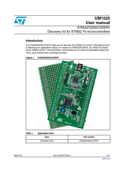
UM1525User manualSTM32F0DISCOVERYDiscovery kit for STM32 F0 microcontrollersIntroductionThe STM32F0DISCOVERY helps you to discover the STM32 F0 Cortex™-M0 features andto develop your applications easily. It is based on STM32F051R8T6, an STM32 F0 series32-bit ARM® Cortex™ microcontroller, and includes an ST-LINK/V2 embedded debug tool,LEDs, push buttons and a prototyping board.Figure 1.STM32F0DISCOVERYTable 1.Applicable toolsType Part numberEvaluation tools STM32F0DISCOVERYMay 2012Doc ID 022910 Rev 21/41Contents UM1525 Contents1Conventions . . . . . . . . . . . . . . . . . . . . . . . . . . . . . . . . . . . . . . . . . . . . . . . . 62Quick start . . . . . . . . . . . . . . . . . . . . . . . . . . . . . . . . . . . . . . . . . . . . . . . . . 72.1Getting started . . . . . . . . . . . . . . . . . . . . . . . . . . . . . . . . . . . . . . . . . . . . . . 72.2System requirements . . . . . . . . . . . . . . . . . . . . . . . . . . . . . . . . . . . . . . . . . 72.3Development toolchain supporting the STM32F0DISCOVERY . . . . . . . . . 72.4Order code . . . . . . . . . . . . . . . . . . . . . . . . . . . . . . . . . . . . . . . . . . . . . . . . . 7 3Features . . . . . . . . . . . . . . . . . . . . . . . . . . . . . . . . . . . . . . . . . . . . . . . . . . . 84Hardware and layout . . . . . . . . . . . . . . . . . . . . . . . . . . . . . . . . . . . . . . . . . 94.1STM32F051R8T6 microcontroller . . . . . . . . . . . . . . . . . . . . . . . . . . . . . . 124.2Embedded ST-LINK/V2 . . . . . . . . . . . . . . . . . . . . . . . . . . . . . . . . . . . . . . 144.2.1Using ST-LINK/V2 to program/debug the STM32 F0 on board . . . . . . . 154.2.2Using ST-LINK/V2 to program/debug an external STM32 application . . 164.3Power supply and power selection . . . . . . . . . . . . . . . . . . . . . . . . . . . . . . 174.4LEDs . . . . . . . . . . . . . . . . . . . . . . . . . . . . . . . . . . . . . . . . . . . . . . . . . . . . 174.5Push buttons . . . . . . . . . . . . . . . . . . . . . . . . . . . . . . . . . . . . . . . . . . . . . . 174.6JP2 (Idd) . . . . . . . . . . . . . . . . . . . . . . . . . . . . . . . . . . . . . . . . . . . . . . . . . . 174.7OSC clock . . . . . . . . . . . . . . . . . . . . . . . . . . . . . . . . . . . . . . . . . . . . . . . . 184.7.1OSC clock supply . . . . . . . . . . . . . . . . . . . . . . . . . . . . . . . . . . . . . . . . . 184.7.2OSC 32 KHz clock supply . . . . . . . . . . . . . . . . . . . . . . . . . . . . . . . . . . . 184.8Solder bridges . . . . . . . . . . . . . . . . . . . . . . . . . . . . . . . . . . . . . . . . . . . . . 194.9Extension connectors . . . . . . . . . . . . . . . . . . . . . . . . . . . . . . . . . . . . . . . . 205Connecting modules on the prototyping board . . . . . . . . . . . . . . . . . . 275.1Mikroelektronica accessory boards . . . . . . . . . . . . . . . . . . . . . . . . . . . . . 275.2ST MEMS “adapter boards”, standard DIL24 socket . . . . . . . . . . . . . . . . 305.3Arduino shield boards . . . . . . . . . . . . . . . . . . . . . . . . . . . . . . . . . . . . . . . . 33 6Mechanical drawing . . . . . . . . . . . . . . . . . . . . . . . . . . . . . . . . . . . . . . . . 36 7Electrical schematics . . . . . . . . . . . . . . . . . . . . . . . . . . . . . . . . . . . . . . . 37 2/41Doc ID 022910 Rev 2UM1525Contents 8Revision history . . . . . . . . . . . . . . . . . . . . . . . . . . . . . . . . . . . . . . . . . . . 40Doc ID 022910 Rev 23/41List of tables UM1525 List of tablesTable 1.Applicable tools. . . . . . . . . . . . . . . . . . . . . . . . . . . . . . . . . . . . . . . . . . . . . . . . . . . . . . . . . . . 1 Table 2.ON/OFF conventions . . . . . . . . . . . . . . . . . . . . . . . . . . . . . . . . . . . . . . . . . . . . . . . . . . . . . . 6 Table 3.Jumper states. . . . . . . . . . . . . . . . . . . . . . . . . . . . . . . . . . . . . . . . . . . . . . . . . . . . . . . . . . . 14 Table 4.Debug connector CN3 (SWD) . . . . . . . . . . . . . . . . . . . . . . . . . . . . . . . . . . . . . . . . . . . . . . 16 Table 5.Solder bridge settings. . . . . . . . . . . . . . . . . . . . . . . . . . . . . . . . . . . . . . . . . . . . . . . . . . . . . 19 Table 6.MCU pin description versus board function . . . . . . . . . . . . . . . . . . . . . . . . . . . . . . . . . . . . 20 Table 7.Connecting using mikroBUS™. . . . . . . . . . . . . . . . . . . . . . . . . . . . . . . . . . . . . . . . . . . . . . 27 Table 8.Connecting using IDC10. . . . . . . . . . . . . . . . . . . . . . . . . . . . . . . . . . . . . . . . . . . . . . . . . . . 28 Table 9.Connecting with a DIL24 board . . . . . . . . . . . . . . . . . . . . . . . . . . . . . . . . . . . . . . . . . . . . . 30 Table 10.Supported MEMS adapter boards . . . . . . . . . . . . . . . . . . . . . . . . . . . . . . . . . . . . . . . . . . . 32 Table 11.Connecting with Arduino shields. . . . . . . . . . . . . . . . . . . . . . . . . . . . . . . . . . . . . . . . . . . . . 33 Table 12.Document revision history . . . . . . . . . . . . . . . . . . . . . . . . . . . . . . . . . . . . . . . . . . . . . . . . . 40 4/41Doc ID 022910 Rev 2UM1525List of figures List of figuresFigure 1.STM32F0DISCOVERY. . . . . . . . . . . . . . . . . . . . . . . . . . . . . . . . . . . . . . . . . . . . . . . . . . . . . 1 Figure 2.Hardware block diagram . . . . . . . . . . . . . . . . . . . . . . . . . . . . . . . . . . . . . . . . . . . . . . . . . . . 9 Figure 3.Top layout . . . . . . . . . . . . . . . . . . . . . . . . . . . . . . . . . . . . . . . . . . . . . . . . . . . . . . . . . . . . . 10 Figure 4.Bottom layout . . . . . . . . . . . . . . . . . . . . . . . . . . . . . . . . . . . . . . . . . . . . . . . . . . . . . . . . . . . 11 Figure 5.STM32F051R8T6 package. . . . . . . . . . . . . . . . . . . . . . . . . . . . . . . . . . . . . . . . . . . . . . . . . 12 Figure 6.STM32F051R8T6 block diagram . . . . . . . . . . . . . . . . . . . . . . . . . . . . . . . . . . . . . . . . . . . . 13 Figure 7.Typical configuration . . . . . . . . . . . . . . . . . . . . . . . . . . . . . . . . . . . . . . . . . . . . . . . . . . . . . 14 Figure 8.STM32F0DISCOVERY connections image . . . . . . . . . . . . . . . . . . . . . . . . . . . . . . . . . . . . 15 Figure 9.ST-LINK connections image. . . . . . . . . . . . . . . . . . . . . . . . . . . . . . . . . . . . . . . . . . . . . . . . 16 Figure ing IDC10 and mikroBUS™ connectors. . . . . . . . . . . . . . . . . . . . . . . . . . . . . . . . . . . . . 29 Figure 11.DIL24 socket connections. . . . . . . . . . . . . . . . . . . . . . . . . . . . . . . . . . . . . . . . . . . . . . . . . . 31 Figure 12.Arduino shield board connections. . . . . . . . . . . . . . . . . . . . . . . . . . . . . . . . . . . . . . . . . . . . 35 Figure 13.STM32F0DISCOVERY mechanical drawing . . . . . . . . . . . . . . . . . . . . . . . . . . . . . . . . . . . 36 Figure 14.STM32F0DISCOVERY. . . . . . . . . . . . . . . . . . . . . . . . . . . . . . . . . . . . . . . . . . . . . . . . . . . . 37 Figure 15.ST-LINK/V2 (SWD only). . . . . . . . . . . . . . . . . . . . . . . . . . . . . . . . . . . . . . . . . . . . . . . . . . . 38 Figure 16.MCU . . . . . . . . . . . . . . . . . . . . . . . . . . . . . . . . . . . . . . . . . . . . . . . . . . . . . . . . . . . . . . . . . . 39Doc ID 022910 Rev 25/41Conventions UM1525 1 ConventionsTable 2 provides the definition of some conventions used in the present document.Table 2.ON/OFF conventionsConvention DefinitionJumper JP1 ON Jumper fittedJumper JP1 OFF Jumper not fittedSolder bridge SBx ON SBx connections closed by solderSolder bridge SBx OFF SBx connections left open6/41Doc ID 022910 Rev 2UM1525Quick startDoc ID 022910 Rev 27/412 Quick startThe STM32F0DISCOVERY is a low-cost and easy-to-use development kit to quicklyevaluate and start development with an STM32 F0 series microcontroller.Before installing and using the product, please accept the Evaluation Product License Agreement from /stm32f0discovery .For more information on the STM32F0DISCOVERY and for demonstration software, visit /stm32f0discovery .2.1 Getting startedFollow the sequence below to configure the STM32F0DISCOVERY board and launch theDISCOVER application:1.Check jumper position on the board, JP2 on, CN2 on (Discovery selected).2.Connect the STM32F0DISCOVERY board to a PC with a USB cable ‘type A to mini-B’ through USB connector CN1 to power the board. Red LED LD1 (PWR) and LD2 (COM) light up and green LED LD3 blinks.3. Press user button B1 (bottom left corner of the board).4. Observe how the green LED LD3 blinking changes according to USER button B1 clicks.5. Each click on USER button B1 is confirmed by the blue LED LD4.6. To study or modify the DISCOVER project related to this demo, visit /stm32f0discovery and follow the tutorial.7. Discover the STM32F0 features, download and execute programs proposed in the list of projects.8.Develop your own application using available examples.2.2 System requirements●Windows PC (XP , Vista, 7)●USB type A to Mini-B USB cable2.3 Development toolchain supporting the STM32F0DISCOVERY●Altium®, TASKING™ VX-toolset ●ARM®, Atollic TrueSTUDIO®●IAR™, EWARM (IAR Embedded Workbench®)●Keil™, MDK-ARM™2.4 Order codeTo order the STM32F0 Discovery kit, use the order code STM32F0DISCOVERY.Features UM15258/41Doc ID 022910 Rev 23 FeaturesThe STM32F0DISCOVERY kit offers the following features:●STM32F051R8T6 microcontroller featuring 64 KB Flash, 8 KB RAM in an LQFP64 package●On-board ST -LINK/V2 with selection mode switch to use the kit as a standalone ST -LINK/V2 (with SWD connector for programming and debugging)●Board power supply: through USB bus or from an external 5 V supply voltage ●External application power supply: 3 V and 5 V ●Four LEDs:–LD1 (red) for 3.3 V power on–LD2 (red/green) for USB communication –LD3 (green) for PC9 output –LD4 (blue) for PC8 output●Two push buttons (user and reset)●Extension header for LQFP64 I/Os for quick connection to prototyping board and easy probing.●An additional board is provided with the kit which can be connected to the extension connector for even easier prototyping and probing.●A large number of free ready-to-run application firmware examples are available on /stm32f0discovery to support quick evaluation and development.UM1525Hardware and layout 4 Hardware and layoutThe STM32F0DISCOVERY is designed around the STM32F051R8T6 microcontroller in a64-pin LQFP package.Figure 2 illustrates the connections between the STM32F051R8T6 and its peripherals (ST-LINK/V2, push button, LEDs and connectors).Figure 3 and Figure 4 help you to locate these features on the STM32F0DISCOVERY.Doc ID 022910 Rev 29/41Hardware and layout UM1525Note:Pin 1 of CN2, CN3, P1 and P2 connectors are identified by a square.10/41Doc ID 022910 Rev 2Doc ID 022910 Rev 211/4112/41Doc ID 022910 Rev 24.1 STM32F051R8T6 microcontrollerThis 32-bit low- and medium-density advanced ARM™ MCU with a high-performance ARMCortex™-M0 32-bit RISC core has 64 Kbytes Flash, 8 Kbytes RAM, RTC, timers, ADC, DAC, comparators and communication interfaces.Figure 5.STM32F051R8T6 package-3 634- & 2 4+BYTE OF &LASH MEMORY+BYTES OF 2!-,1&0 X MMThe STM32 F0 delivers 32-bit performance and STM32 DNA essentials into applications typically addressed by 8- or 16-bit microcontrollers. It benefits from the combination of real-time performance, low-power operation, advanced architecture and peripherals associated to the STM32 ecosystem, which has made the STM32 a reference in the market. Now all this is accessible for cost-sensitive applications. The STM32 F0 offers unparalleled flexibility and scalability for home entertainment products, appliances, and industrial equipment.This device provides the following benefits.●Superior code execution for better performance and excellent code efficiency for reduced embedded memory usage●High-performance connectivity and advanced analog peripherals to support a wide range of applications●Flexible clock options and low power modes with fast wake-up for low power consumptionIt has the following key features:●Core and operating conditions –ARM® Cortex™-M0 0.9 DMIPS/MHz up to 48 MHz –1.8/2.0 to3.6 V supply range ●High-performance connectivity – 6 Mbit/s USART–18 Mbit/s SPI with 4- to 16-bit data frame – 1 Mbit/s I²C fast-mode plus –HDMICEC●Enhanced control –1x 16-bit 3-phase PWM motor control timer –5x 16-bit PWM timers –1x 16-bit basic timer –1x 32-bit PWM timer –12 MHz I/O togglingDoc ID 022910 Rev 213/4114/41Doc ID 022910 Rev 24.2 Embedded ST-LINK/V2The ST -LINK/V2 programming and debugging tool is integrated on theSTM32F0DISCOVERY. The embedded ST -LINK/V2 can be used in 2 different ways according to the jumper states (see Table 3):●Program/debug the MCU on board,●Program/debug an MCU in an external application board using a cable connected to SWD connector CN3.The embedded ST -LINK/V2 supports only SWD for STM32 devices. For information about debugging and programming features refer to user manual UM1075 (ST -LINK/V2 in-circuit debugger/programmer for STM8 and STM32) which describes in detail all the ST -LINK/V2 features.Table 3.Jumper statesJumper stateDescriptionBoth CN2 jumpers ONST -LINK/V2 functions enabled for on board programming (default) Both CN2 jumpers OFFST -LINK/V2 functions enabled for application through external CN3 connector (SWD supported)4.2.1 Using ST-LINK/V2 to program/debug the STM32 F0 on boardTo program the STM32 F0 on board, simply plug in the two jumpers on CN2, as shown inFigure 8 in red, but do not use the CN3 connector as that could disturb communication withthe STM32F051R8T6 of the STM32F0DISCOVERY.Figure 8.STM32F0DISCOVERY connections imageDoc ID 022910 Rev 215/414.2.2 Using ST-LINK/V2 to program/debug an external STM32 applicationIt is very easy to use the ST-LINK/V2 to program the STM32 on an external application.Simply remove the 2 jumpers from CN2 as shown in Figure 9, and connect your applicationto the CN3 debug connector according to Table 4.Note:SB19 and SB22 must be OFF if you use CN3 pin 5 in your external application.Table 4.Debug connector CN3 (SWD)Pin CN3Designation1 VDD_TARGET VDD from application2 SWCLK SWD clock3 GND Ground4 SWDIO SWD data input/output5 NRST RESET of target MCU6 SWO ReservedFigure 9.ST-LINK connections image16/41Doc ID 022910 Rev 24.3 Power supply and power selectionThe power supply is provided either by the host PC through the USB cable, or by an external5V power supply.The D1 and D2 diodes protect the 5V and 3V pins from external power supplies:●5V and 3V can be used as output power supplies when another application board isconnected to pins P1 and P2.In this case, the 5V and 3V pins deliver a 5V or 3V power supply and powerconsumption must be lower than 100 mA.●5V can also be used as input power supplies e.g. when the USB connector is notconnected to the PC.In this case, the STM32F0DISCOVERY board must be powered by a power supply unitor by auxiliary equipment complying with standard EN-60950-1: 2006+A11/2009, andmust be Safety Extra Low Voltage (SELV) with limited power capability.4.4LEDs●LD1 PWR: Red LED indicates that the board is powered.●LD2 COM: Tricolor LED (COM) advises on the communication status as follows:–Slow blinking Red LED/Off: At power on before USB initialization–Fast blinking Red LED/Off: After the first correct communication between PC and STLINK/V2 (enumeration)–Red LED On: When initialization between PC and ST-LINK/V2 is successfully finished–Green LED On: After successful target communication initialization–Blinking Red/Green LED: During communication with target–Red LED On: Communication finished and OK–Orange LED On: Communication failure●User LD3: Green user LED connected to the I/O PC9 of the STM32F051R8T6.●User LD4: Blue user LED connected to the I/O PC8 of the STM32F051R8T6.4.5 Pushbuttons●B1 USER: User push button connected to the I/O PA0 of the STM32F051R8T6.●B2 RESET: Push button used to RESET the STM32F051R8T6.4.6 JP2(Idd)Jumper JP2, labeled Idd, allows the consumption of STM32F051R8T6 to be measured byremoving the jumper and connecting an ammeter.●Jumper on: STM32F051R8T6 is powered (default).●Jumper off: an ammeter must be connected to measure the STM32F051R8T6 current,(if there is no ammeter, the STM32F051R8T6 is not powered).Doc ID 022910 Rev 217/414.7 OSCclocksupplyclock4.7.1 OSCPF0 and PF1 can be used as GPIO or as HSE oscillator. By default these I/Os areconfigured as GPIO, so SB16 and SB17 are closed, SB18 is open and R22, R23, C13 andC14 are not populated.An external HSE clock can be provided to the MCU in three ways:●MCO from ST-LINK. From MCO of the STM32F103. This frequency cannot bechanged, it is fixed at 8 MHz and connected to PF0-OSC_IN of the STM32F051R8T6.Configuration needed:–SB16, SB18 CLOSED–R22,R23removed–SB17 OPEN●Oscillator onboard. From X2 crystal (not provided). For typical frequencies and itscapacitors and resistors, please refer to the STM32F051R8T6 Datasheet.Configuration needed:–SB16, SB17 SB18 OPEN–R22, R23, C13, C14 soldered●Oscillator from external PF0. From external oscillator through pin 7 of the P1connector. Configuration needed:–SB16, SB17 CLOSED–SB18 OPEN–R22 and R23 removed32 KHz clock supply4.7.2 OSCPC14 and PC15 can be used as GPIO or as LSE oscillator. By default these I/Os areconfigured as GPIO, so SB20 & SB21 are closed and X3, R24, R25 are not populated.An external LSE clock can be provided to the MCU in two ways:●Oscillator onboard. From X3 crystal (not provided). Configuration needed:–SB20, SB21 OPEN–C15, C16, R24 and R25 soldered.●Oscillator from external PC14. From external oscillator trough the pin 5 of P1connector. Configuration needed:–SB20, SB21 CLOSED–R24 and R25 removed18/41Doc ID 022910 Rev 2Doc ID 022910 Rev 219/414.8 Solder bridgesTable 5.Solder bridge settingsBridgeState (1) DescriptionSB16,17(X2 crystal)(2)2.OSC_IN clock comes from MCO if SB18 is ON and SB16,17 are OFFand comes from X2 if SB18 is OFF and SB16,17 are ON.OFF X2, C13, C14, R22 and R23 provide a clock. PF0, PF1 are disconnected from P1.ON PF0, PF1 are connected to P1 (R22, R23 and SB18 must not be fitted). SB6,8,10,12 (Default) ON Reserved, do not modify. SB5,7,9,11 (Reserved) OFF Reserved, do not modify.SB20,21(X3 crystal)OFF X3, C15, C16, R24 and R25 deliver a 32 KHz clock. PC14, PC15 are not connected to P1.ON PC14, PC15 are only connected to P1 (R24, R25 must not be fitted).SB4(B2-RESET) ON B2 push button is connected to the NRST pin of the STM32F051R8T6 MCU.OFF B2 push button is not connected the NRST pin of the STM32F051R8T6 MCU.SB3(B1-USER)ON B1 push button is connected to P A0. OFFB1 push button is not connected to P A0. SB1(VBA T powered from VDD) ON VBA T is permanently powered from VDD.OFF VBA T is not powered from VDD but pin3 of P1.SB14,15(RX,TX) OFF Reserved, do not modify. ON Reserved, do not modify.SB19(NRST) ON NRST signal of the CN3 connector is connected to the NRST pin of the STM32F051R8T6 MCU.OFF NRST signal of the CN3 connector is not connected to the NRST pin of the STM32F051R8T6 MCU.SB22(T_SWO) ON SWO signal of the CN3 connector is connected to PB3. OFF SWO signal is not connected.SB13(STM_RST) OFF No incidence on STM32F103C8T6 (ST -LINK/V2) NRST signal. ON STM32F103C8T6 (ST -LINK/V2) NRST signal is connected to GND. SB2(BOOT0) ON BOOT0 signal of the STM32F051R8T6 MCU is held low through a 510 Ohm pull-down resistor.OFF BOOT0 signal of the STM32F051R8T6 MCU can be set high through a 10 KOhm pull-up resistor R27 to solder.SB18(MCO)(2)ON Provides the 8 MHz for OSC_IN from MCO of STM32F103C8T6.OFFSee SB16, SB17 description.1.Default SBx state is shown in bold.20/41Doc ID 022910 Rev 24.9 Extension connectorsThe male headers P1 and P2 can connect the STM32F0DISCOVERY to a standardprototyping/wrapping board. STM32F051R8T6 GPI/Os are available on these connectors. P1 and P2 can also be probed by an oscilloscope, logical analyzer or voltmeter.Table 6.MCU pin description versus board function (page 1 of 7)MCU pinBoard functionMain function Alternate functionsLQFP64Push buttonLEDSWDOSCFree I/OPower supplyCN3P1P2BOOT0BOOT0606NRSTNRST 7RESET NRST510P A02_CTS, IN0,2_CH1_ETR, 1_INM6, 1_OUT ,TSC_G1_IO1, RTC_T AMP2, WKUP114USER15P A12_RTS, IN1, 2_CH2, 1_INP ,TSC_G1_IO2, EVENTOUT 1516P A22_TX, IN2, 2_CH3, 15_CH1, 2_INM6, 2_OUT ,TSC_G1_IO31617P A32_RX, IN3, 2_CH4, 15_CH2, 2_INP ,TSC_G1_IO4,1718UM1525Hardware and layoutDoc ID 022910 Rev 221/41P A41_NSS / 1_WS, 2_CK, IN4,14_CH1, DAC1_OUT, 1_INM4, 2_INM4,TSC_G2_IO12021P A51_SCK / 1_CK, CEC, IN5,2_CH1_ETR, (DAC2_OUT), 1_INM5, 2_INM5,TSC_G2_IO22122P A61_MISO / 1_MCK, IN6, 3_CH1, 1_BKIN, 16_CH1, 1_OUT ,TSC_G2_IO3, EVENTOUT 2223P A71_MOSI / 1_SD, IN7, 3_CH2, 14_CH1, 1_CH1N, 17_CH1, 2_OUT ,TSC_G2_IO4, EVENTOUT 2324P A81_CK, 1_CH1,EVENTOUT, MCO 4125P A91_TX, 1_CH2, 15_BKIN, TSC_G4_IO14224Table 6.MCU pin description versus board function (page 2 of 7)MCU pinBoard functionMain function Alternate functionsLQFP64Push buttonLEDSWDOSCFree I/OPower supplyCN3P1P2Hardware and layoutUM152522/41Doc ID 022910 Rev 2P A101_RX, 1_CH3, 17_BKIN, TSC_G4_IO24323P A111_CTS, 1_CH4, 1_OUT ,TSC_G4_IO3, EVENTOUT 4422P A121_RTS, 1_ETR, 2_OUT ,TSC_G4_IO4, EVENTOUT 4521P A13IR_OUT, SWDA T 46SWDIO 420P A142_TX, SWCLK 49SWCLK217P A151_NSS / 1_WS, 2_RX,2_CH1_ETR, EVENTOUT 5016PB0IN8, 3_CH3, 1_CH2N,TSC_G3_IO2, EVENTOUT 2627PB1IN9, 3_CH4, 14_CH1, 1_CH3N, TSC_G3_IO32728PB2 or NPOR (1.8V mode)TSC_G3_IO42829PB31_SCK / 1_CK, 2_CH2,TSC_G5_IO1, EVENTOUT55SWO611Table 6.MCU pin description versus board function (page 3 of 7)MCU pinBoard functionMain function Alternate functionsLQFP64Push buttonLEDSWDOSCFree I/OPower supplyCN3P1P2UM1525Hardware and layoutDoc ID 022910 Rev 223/41PB41_MISO / 1_MCK, 3_CH1,TSC_G5_IO2, EVENTOUT 5610PB51_MOSI / 1_SD, 1_SMBA, 16_BKIN, 3_CH2579PB61_SCL, 1_TX, 16_CH1N, TSC_G5_IO3588PB71_SDA, 1_RX, 17_CH1N, TSC_G5_IO4597PB81_SCL, CEC, 16_CH1, TSC_SYNC 614PB91_SDA,IR_EVENTOUT, 17_CH1, EVENTOUT 623PB102_SCL, CEC, 2_CH3, SYNC 2930PB112_SDA, 2_CH4, G6_IO1, EVENTOUT 3031PB122_NSS, 1_BKIN, G6_IO2, EVENTOUT 3332PB132_SCK, 1_CH1N, G6_IO33432Table 6.MCU pin description versus board function (page 4 of 7)MCU pinBoard functionMain function Alternate functionsLQFP64Push buttonLEDSWDOSCFree I/OPower supplyCN3P1P2Hardware and layoutUM152524/41Doc ID 022910 Rev 2PB142_MISO, 1_CH2N, 15_CH1, G6_IO43531PB152_MOSI, 1_CH3N, 15_CH1N, 15_CH2, RTC_REFIN 3630PC0IN10,EVENTOUT 811PC1IN11,EVENTOUT 912PC2IN12,EVENTOUT 1013PC3IN13,EVENTOUT 1114PC4IN14,EVENTOUT 2425PC5IN15,TSC_G3_IO12526PC63_CH13729PC73_CH23828PC83_CH339BLUE 27PC93_CH440GREEN26PC105115PC115214PC125313PC13RTC_T AMP1, RTC_TS, RTC_OUT , WKUP224Table 6.MCU pin description versus board function (page 5 of 7)MCU pinBoard functionMain function Alternate functionsLQFP64Push buttonLEDSWDOSCFree I/OPower supplyCN3P1P2UM1525Hardware and layoutDoc ID 022910 Rev 225/41PC14-OSC32_ INOSC32_IN 3OSC32_IN 5PC15-OSC32_OUT OSC32_OUT 4OSC32_OUT6PD23_ETR 5412PF0-OSC_IN OSC_IN5OSC_IN 7PF1-OSC_ OUT OSC_OUT 6OSC_OUT8PF4EVENTOUT 1819PF5EVENTOUT 1920PF62_SCL 4719PF72_SDA 4818VBA T VBA T13VDD_164VDD_232VDDA 13VSS_163VSS_231VSSA125V 13V 1VDD 5GND 22GNDGND3Table 6.MCU pin description versus board function (page 6 of 7)MCU pinBoard functionMain function Alternate functionsLQFP64Push buttonLEDSWDOSCFree I/OPower supplyCN3P1P2Hardware and layout UM152526/41Doc ID 022910 Rev 2GND9 GND3333Table 6.MCU pin description versus board function (page 7 of 7) MCU pin Board functionMain function Alternatefunctions LQFP64Push button LED SWD OSC Free I/O Power supply CN3P1 P25 Connecting modules on the prototyping boardThis section gives some examples of how to connect ready-to-use modules available fromdifferent manufacturers to the STM32F0DISCOVERY kit via the prototyping board includedin the kit.Software examples, based on the connections described below, are available at/stm32f0discovery.5.1 Mikroelektronica accessory boardsMikroelektronika, , has specified two standard connectors for theiraccessory boards, named mikroBUS™ (/mikrobus_specs.pdf) andIDC10.MikroBUS™ is a 16-pin connector to connect accessory boards very quickly and easily to amicrocontroller board through SPI, USART or I2C communications, along with additionalpins such as Analog Input, PWM and Interrupt.The set of mikroElektronika boards compatible with mikroBUS™ is called “Click boards”.IDC10 is a 10-pin connector to connect the general purpose I/O of an MCU to otheraccessory boards.The tables below are one solution for connecting mikroBUS™ and IDC boards to theSTM32F0DISCOVERY; this solution used in the different examples is available at/stm32f0discovery.Table 7.Connecting using mikroBUS™Mikroelektronica mikroBUS™STM32F0DISCOVERYPin Description Pin DescriptionAN Analog pin P A4DAC1_OUTRST Reset pin PB13GPIO OUTPUT (5V tolerant)CS SPI Chip Select line P A11GPIO OUTPUT (5V tolerant)SCK SPI Clock line PB3SPI1_SCKMISO SPI Slave Output line PB4SPI1_MISOMOSI SPI Slave Input line PB5SPI1_MOSIPWM PWM output line P A8TIM1_CH1INT Hardware Interrupt line PB12GPIO INPUT EXTI (5V tolerant)RX UART Receive line P A3USART2_RXTX UART Transmit line P A2USART2_TXSCL I2C Clock line PF6I2C2_SCLSDA I2C Data line PF7I2C2_SDA5V VCC 5V power line5V Power lineDoc ID 022910 Rev 227/41Table 8.Connecting using IDC10Mikroelektronica IDC10 connector STM32F0DISCOVERYP0GPIO PC0GPIO OUTPUT (3.3V tolerant)P1GPIO PC1GPIO OUTPUT (3.3V tolerant)P2GPIO PC2GPIO OUTPUT (3.3V tolerant)P3GPIO PC3GPIO OUTPUT (3.3V tolerant)P4GPIO PC4GPIO OUTPUT (3.3V tolerant)P5GPIO PC5GPIO OUTPUT (3.3V tolerant)P6GPIO PC6GPIO OUTPUT (5V tolerant)P7GPIO PC7GPIO OUTPUT (5V tolerant)VCC VCC 5V power line3V VDDGND Reference Ground GND VSSP0GPIO PC0GPIO OUTPUT (3.3V tolerant)P1GPIO PC1GPIO OUTPUT (3.3V tolerant)P2GPIO PC2GPIO OUTPUT (3.3V tolerant)P3GPIO PC3GPIO OUTPUT (3.3V tolerant) 28/41Doc ID 022910 Rev 2。
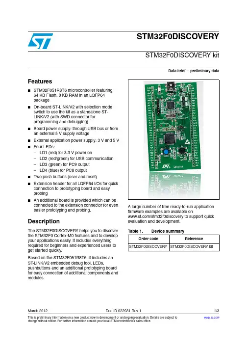
This is preliminary information on a new product now in development or undergoing evaluation. Details are subject to change without notice. For further information contact your local STMicroelectronics sales office.March 2012Doc ID 022931 Rev 11/3STM32F0DISCOVERYSTM32F0DISCOVERY kitData brief preliminary dataFeatures■STM32F051R8T6 microcontroller featuring 64KB Flash, 8 KB RAM in an LQFP64 package■On-board ST-LINK/V2 with selection mode switch to use the kit as a standalone ST-LINK/V2 (with SWD connector for programming and debugging)■Board power supply: through USB bus or from an external 5 V supply voltage■External application power supply: 3 V and 5 V ■Four LEDs:–LD1 (red) for 3.3 V power on–LD2 (red/green) for USB communication –LD3 (green) for PC9 output –LD4 (blue) for PC8 output ■Two push buttons (user and reset)■Extension header for all LQFP64 I/Os for quick connection to prototyping board and easy probing■An additional board is provided which can be connected to the extension connector for even easier prototyping and probing.DescriptionThe STM32F0DISCOVERY helps you to discover the STM32F0 Cortex-M0 features and to develop your applications easily. It includes everything required for beginners and experienced users to get started quickly.Based on the STM32F051R8T6, it includes an ST -LINK/V2 embedded debug tool, LEDs,pushbuttons and an additional prototyping board for easy connection of additional components and modules.A large number of free ready-to-run application firmware examples are available on/stm32f0discovery to support quick evaluation and development.Table 1.Device summaryOrder codeReferenceSTM32F0DISCOVERY STM32F0DISCOVERY kitSystem requirements STM32F0DISCOVERY2/3Doc ID 022931 Rev 11 System requirements●Windows PC (XP , Vista, 7)●USB type A to Mini-B cable2 Development toolchains●Altium TASKING™ VX-Toolset ●Atollic T rueSTUDIO®●IAR, EWARM ●Keil™, MDK-ARM3 Demonstration softwareThe demonstration software is preloaded in the board Flash memory. It uses the user buttonB1 to change the blinking frequency of the green LED LD3. Each click on the button is confirmed by the blue LED LD4.The latest versions of the demonstration source code and associated documentation can be downloaded from /stm32f0discovery.STM32F0DISCOVERYPlease Read Carefully:Information in this document is provided solely in connection with ST products. STMicroelectronics NV and its subsidiaries (“ST”) reserve the right to make changes, corrections, modifications or improvements, to this document, and the products and services described herein at any time, without notice.All ST products are sold pursuant to ST’s terms and conditions of sale.Purchasers are solely responsible for the choice, selection and use of the ST products and services described herein, and ST assumes no liability whatsoever relating to the choice, selection or use of the ST products and services described herein.No license, express or implied, by estoppel or otherwise, to any intellectual property rights is granted under this document. If any part of this document refers to any third party products or services it shall not be deemed a license grant by ST for the use of such third party products or services, or any intellectual property contained therein or considered as a warranty covering the use in any manner whatsoever of such third party products or services or any intellectual property contained therein.UNLES S OTHERWIS E S ET FORTH IN S T’S TERMS AND CONDITIONS OF S ALE S T DIS CLAIMS ANY EXPRES S OR IMPLIED WARRANTY WITH RES PECT TO THE US E AND/OR S ALE OF S T PRODUCTS INCLUDING WITHOUT LIMITATION IMPLIED WARRANTIES OF MERCHANTABILITY, FITNESS FOR A PARTICULAR PURPOSE (AND THEIR EQUIVALENTS UNDER THE LAWS OF ANY JURISDICTION), OR INFRINGEMENT OF ANY PATENT, COPYRIGHT OR OTHER INTELLECTUAL PROPERTY RIGHT. UNLES S EXPRES S LY APPROVED IN WRITING BY TWO AUTHORIZED S T REPRES ENTATIVES, S T PRODUCTS ARE NOT RECOMMENDED, AUTHORIZED OR WARRANTED FOR USE IN MILITARY, AIR CRAFT, SPACE, LIFE SAVING, OR LIFE SUSTAINING APPLICATIONS, NOR IN PRODUCTS OR SYSTEMS WHERE FAILURE OR MALFUNCTION MAY RESULT IN PERSONAL INJURY, DEATH, OR SEVERE PROPERTY OR ENVIRONMENTAL DAMAGE. ST PRODUCTS WHICH ARE NOT SPECIFIED AS "AUTOMOTIVE GRADE" MAY ONLY BE USED IN AUTOMOTIVE APPLICATIONS AT USER’S OWN RISK.Resale of ST products with provisions different from the statements and/or technical features set forth in this document shall immediately void any warranty granted by ST for the ST product or service described herein and shall not create or extend in any manner whatsoever, any liability of ST.ST and the ST logo are trademarks or registered trademarks of ST in various countries.Information in this document supersedes and replaces all information previously supplied.The ST logo is a registered trademark of STMicroelectronics. All other names are the property of their respective owners.© 2012 STMicroelectronics - All rights reservedSTMicroelectronics group of companiesAustralia - Belgium - Brazil - Canada - China - Czech Republic - Finland - France - Germany - Hong Kong - India - Israel - Italy - Japan - Malaysia - Malta - Morocco - Philippines - Singapore - Spain - Sweden - Switzerland - United Kingdom - United States of AmericaDoc ID 022931 Rev 13/3。
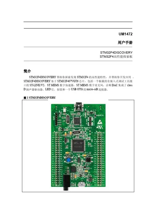
UM1472用户手册STM32F4DISCOVERYSTM32F4高性能探索板简介STM32F4DISCOVERY帮助你探索发现STM32F4的高性能特性,并帮助你开发应用。
STM32F4DISCOVERY基于STM32F407VGT6芯片,包括一个板载的有嵌入式调试工具接口的ST-LINK/V2,ST MEMS数字加速器,ST MEMS 数字麦克风,音频DAC集成了class D扬声器驱动器,LED灯,按钮和一个USB OTG的micro-AB连接器。
图 1 STM32F4DISCOVERYSTM32F4DISCOVERY系统要求目录1 约定 (5)2 快速入门 (6)开始 (6)2.1 系统要求 (7)2.2 支持STM32F4DISCOVERY的开发工具链 (7)2.3 订单编码 (7)3 特性 (7)4 硬件和布局 (8)4.1 STM32F407VGT6微控制器 (10)4.2 嵌入的ST-LINK/V2 (13)4.2.1 使用ST-LINK/V2编程/调试板上STM32F4 (14)4.2.2 使用ST-LINK/V2编程/调试外部STM32应用 (15)4.3 电源和电源选择 (16)4.4 LED (16)4.5 按键 (16)4.6 板上音频功能 (17)4.7 支持USB OTG (17)4.8 运动传感器(ST MEMS LIS302DL) (17)4.9 JP1 (Idd) (17)4.10 锡桥 (18)4.11 扩展连接 (19)5 机械制图 (29)6 电气原理图 (31)- 2 -电气原理图STM32F4DISCOVERY 表列表 1 ON/OFF 约定 (5)表 2 跳线状态 (13)表 3 调试连接器CN2 (SWD) (15)表 4 锡桥 (18)表 5 MCU引脚描述对应板子功能 (19)- 3 -STM32F4DISCOVERY系统要求图列图 1 STM32F4DISCOVERY (2)图 2 硬件框图 (9)图 3 顶层布局 (9)图 4 底层布局 (10)图 5 STM32F407VGT6封装 (10)图 6 STM32F407VGT6框图 (12)图 7 典型配置 (13)图 8 STM32F4DISCOVERY连接图 (14)图 9 ST-LINK连接图 (15)图 10 STM32F4DISCOVERY机械制图 (29)图 11 STM32F4DISCOVERY (31)图 12 ST-LPINK/V2(SWD only) (32)图 13 MCU (33)图 14 Audio (34)图 15 USB_OTG_FS (35)图 16 Peripherals (36)- 4 -电气原理图STM32F4DISCOVERY 1 约定表1提供了在本文中使用的一些约定的定义表 1 ON/OFF 约定- 5 -STM32F4DISCOVERY系统要求2 快速入门STM32F4DISCOVERY是一个低成本、易于使用的开发套件,快速评估并开始使用STM32F4高性能微控制器的进行开发。
UM1525User manualSTM32F0DISCOVERYSTM32F0 discovery kitIntroductionThe STM32F0DISCOVERY helps you to discover the STM32F0 Cortex-M0 features and todevelop your applications easily. It is based on an STM32F051R8T6 and includes an ST-LINK/V2 embedded debug tool, LEDs, push buttons and a prototyping board.Figure 1.STM32F0DISCOVERYMarch 2012Doc ID 022910 Rev 11/31Contents UM1525Contents1Conventions . . . . . . . . . . . . . . . . . . . . . . . . . . . . . . . . . . . . . . . . . . . . . . . . 52Quick start . . . . . . . . . . . . . . . . . . . . . . . . . . . . . . . . . . . . . . . . . . . . . . . . . 62.1Getting started . . . . . . . . . . . . . . . . . . . . . . . . . . . . . . . . . . . . . . . . . . . . . . 62.2System requirements . . . . . . . . . . . . . . . . . . . . . . . . . . . . . . . . . . . . . . . . . 62.3Development toolchain supporting the STM32F0DISCOVERY . . . . . . . . . 62.4Order code . . . . . . . . . . . . . . . . . . . . . . . . . . . . . . . . . . . . . . . . . . . . . . . . . 6 3Features . . . . . . . . . . . . . . . . . . . . . . . . . . . . . . . . . . . . . . . . . . . . . . . . . . . 74Hardware and layout . . . . . . . . . . . . . . . . . . . . . . . . . . . . . . . . . . . . . . . . . 84.1STM32F051R8T6 microcontroller . . . . . . . . . . . . . . . . . . . . . . . . . . . . . . 114.2Embedded ST-LINK/V2 . . . . . . . . . . . . . . . . . . . . . . . . . . . . . . . . . . . . . . 134.2.1Using ST-LINK/V2 to program/debug the STM32 F0 on board . . . . . . . 144.2.2Using ST-LINK/V2 to program/debug an external STM32 application . . 154.3Power supply and power selection . . . . . . . . . . . . . . . . . . . . . . . . . . . . . . 164.4LEDs . . . . . . . . . . . . . . . . . . . . . . . . . . . . . . . . . . . . . . . . . . . . . . . . . . . . 164.5Push buttons . . . . . . . . . . . . . . . . . . . . . . . . . . . . . . . . . . . . . . . . . . . . . . 164.6JP2 (Idd) . . . . . . . . . . . . . . . . . . . . . . . . . . . . . . . . . . . . . . . . . . . . . . . . . . 164.7OSC clock . . . . . . . . . . . . . . . . . . . . . . . . . . . . . . . . . . . . . . . . . . . . . . . . 174.7.1OSC clock supply . . . . . . . . . . . . . . . . . . . . . . . . . . . . . . . . . . . . . . . . . 174.7.2OSC 32 KHz clock supply . . . . . . . . . . . . . . . . . . . . . . . . . . . . . . . . . . . 174.8Solder bridges . . . . . . . . . . . . . . . . . . . . . . . . . . . . . . . . . . . . . . . . . . . . . 184.9Extension connectors . . . . . . . . . . . . . . . . . . . . . . . . . . . . . . . . . . . . . . . . 19 5Mechanical drawing . . . . . . . . . . . . . . . . . . . . . . . . . . . . . . . . . . . . . . . . 26 6Electrical schematics . . . . . . . . . . . . . . . . . . . . . . . . . . . . . . . . . . . . . . . 27 7Revision history . . . . . . . . . . . . . . . . . . . . . . . . . . . . . . . . . . . . . . . . . . . 302/31Doc ID 022910 Rev 1UM1525List of tables List of tablesTable 1.ON/OFF conventions . . . . . . . . . . . . . . . . . . . . . . . . . . . . . . . . . . . . . . . . . . . . . . . . . . . . . . 5 Table 2.Jumper states. . . . . . . . . . . . . . . . . . . . . . . . . . . . . . . . . . . . . . . . . . . . . . . . . . . . . . . . . . . 13 Table 3.Debug connector CN3 (SWD) . . . . . . . . . . . . . . . . . . . . . . . . . . . . . . . . . . . . . . . . . . . . . . 15 Table 4.Solder bridge settings. . . . . . . . . . . . . . . . . . . . . . . . . . . . . . . . . . . . . . . . . . . . . . . . . . . . . 18 Table 5.MCU pin description versus board function . . . . . . . . . . . . . . . . . . . . . . . . . . . . . . . . . . . . 19 Table 6.Document revision history . . . . . . . . . . . . . . . . . . . . . . . . . . . . . . . . . . . . . . . . . . . . . . . . . 30Doc ID 022910 Rev 13/31List of figures UM1525 List of figuresFigure 1.STM32F0DISCOVERY. . . . . . . . . . . . . . . . . . . . . . . . . . . . . . . . . . . . . . . . . . . . . . . . . . . . . 1 Figure 2.Hardware block diagram . . . . . . . . . . . . . . . . . . . . . . . . . . . . . . . . . . . . . . . . . . . . . . . . . . . 8 Figure 3.Top layout . . . . . . . . . . . . . . . . . . . . . . . . . . . . . . . . . . . . . . . . . . . . . . . . . . . . . . . . . . . . . . 9 Figure 4.Bottom layout . . . . . . . . . . . . . . . . . . . . . . . . . . . . . . . . . . . . . . . . . . . . . . . . . . . . . . . . . . . 10 Figure 5.STM32F051R8T6 package. . . . . . . . . . . . . . . . . . . . . . . . . . . . . . . . . . . . . . . . . . . . . . . . . 11 Figure 6.STM32F051R8T6 block diagram . . . . . . . . . . . . . . . . . . . . . . . . . . . . . . . . . . . . . . . . . . . . 12 Figure 7.Typical configuration . . . . . . . . . . . . . . . . . . . . . . . . . . . . . . . . . . . . . . . . . . . . . . . . . . . . . 13 Figure 8.STM32F0DISCOVERY connections image . . . . . . . . . . . . . . . . . . . . . . . . . . . . . . . . . . . . 14 Figure 9.ST-Link connections image . . . . . . . . . . . . . . . . . . . . . . . . . . . . . . . . . . . . . . . . . . . . . . . . 15 Figure 10.STM32F0DISCOVERY mechanical drawing . . . . . . . . . . . . . . . . . . . . . . . . . . . . . . . . . . . 26 Figure 11.STM32F0DISCOVERY. . . . . . . . . . . . . . . . . . . . . . . . . . . . . . . . . . . . . . . . . . . . . . . . . . . . 27 Figure 12.ST-LINK/V2 (SWD only). . . . . . . . . . . . . . . . . . . . . . . . . . . . . . . . . . . . . . . . . . . . . . . . . . . 28 Figure 13.MCU . . . . . . . . . . . . . . . . . . . . . . . . . . . . . . . . . . . . . . . . . . . . . . . . . . . . . . . . . . . . . . . . . . 29 4/31Doc ID 022910 Rev 1UM1525Conventions 1 ConventionsTable 1 provides the definition of some conventions used in the present document.Table 1.ON/OFF conventionsConvention DefinitionJumper JP1 ON Jumper fittedJumper JP1 OFF Jumper not fittedSolder bridge SBx ON SBx connections closed by solderSolder bridge SBx OFF SBx connections left openDoc ID 022910 Rev 15/31Quick start UM15256/31Doc ID 022910 Rev 12 Quick startThe STM32F0DISCOVERY is a low-cost and easy-to-use development kit to quicklyevaluate and start a development with an STM32F0 microcontroller.Before installing and using the product, please accept the Evaluation Product License Agreement from /stm32f0discovery.For more information on the STM32F0DISCOVERY and for demonstration software, visit /stm32f0discovery.2.1 Getting startedFollow the sequence below to configure the STM32F0DISCOVERY board and launch theDISCOVER application:1.Check jumper position on the board, JP2 on, CN2 on (DISCOVERY selected).2.Connect the STM32F0DISCOVERY board to a PC with a USB cable ‘type A to mini-B’ through USB connector CN1 to power the board. Red LED LD1 (PWR) and LD2 (COM) light up and green LED LD3 blinks.3. Press user button B1 (bottom left corner of the board).4. Observe how the green LED LD3 blinking changes according to USER button B1 clicks.5. Each click on USER button B1 is confirmed by the blue LED LD4.6. To study or modify the DISCOVER project related to this demo, visit /stm32f0discovery and follow the tutorial.7. Discover the STM32F0 features, download and execute programs proposed in the list of projects.8.Develop your own application using available examples.2.2 System requirements●Windows PC (XP , Vista, 7)●USB type A to Mini-B USB cable2.3 Development toolchain supporting the STM32F0DISCOVERY●Altium, TASKING™ VX-Toolset ●Atollic, TrueSTUDIO ●IAR, EWARM ●Keil™, MDK-ARM2.4 Order codeTo order the STM32F0 discovery kit, use the order code STM32F0DISCOVERY.UM1525FeaturesDoc ID 022910 Rev 17/313 FeaturesThe STM32F0DISCOVERY kit offers the following features:●STM32F051R8T6 microcontroller featuring 64 KB Flash, 8 KB RAM in an LQFP64 package●On-board ST -LINK/V2 with selection mode switch to use the kit as a standalone ST -LINK/V2 (with SWD connector for programming and debugging)●Board power supply: through USB bus or from an external 5 V supply voltage ●External application power supply: 3 V and 5 V ●Four LEDs:–LD1 (red) for 3.3 V power on–LD2 (red/green) for USB communication –LD3 (green) for PC9 output –LD4 (blue) for PC8 output●Two push buttons (user and reset)●Extension header for LQFP64 I/Os for quick connection to prototyping board and easy probing.●An additional board is provided with the kit which can be connected to the extension connector for even easier prototyping and probing.●A large number of free ready-to-run application firmware examples are available on /stm32f0discovery to support quick evaluation and development.Hardware and layout UM1525 4 Hardware and layoutThe STM32F0DISCOVERY is designed around the STM32F051R8T6 microcontroller in a64-pin LQFP package.Figure 2 illustrates the connections between the STM32F051R8T6 and its peripherals (ST-LINK/V2, push button, LEDs and connectors).Figure 3 and Figure 4 help you to locate these features on the STM32F0DISCOVERY.8/31Doc ID 022910 Rev 1UM1525Hardware and layoutNote:Pin 1 of CN2, CN3, P1 and P2 connectors are identified by a square.Doc ID 022910 Rev 19/31Hardware and layout UM152510/31Doc ID 022910 Rev 1Doc ID 022910 Rev 111/314.1 STM32F051R8T6 microcontrollerThis 32-bit low- and medium-density advanced ARM™ MCU has 64 KB Flash, 8 KB RAM,RTC, timers, ADC, DAC, comparators and comm. interfaces.Figure 5.STM32F051R8T6 packageThe STM32 F0 delivers 32-bit performance and STM32 DNA essentials into applications typically addressed by 8- or 16-bit microcontrollers. It benefits from the combination of real-time performance, low-power operation, advanced architecture and peripherals associated to the STM32 ecosystem, which has made the STM32 a reference in the market. Now all this is accessible for cost-sensitive applications. The STM32 F0 offers unparalleled flexibility and scalability for home-entertainment products, appliances, and industrial equipment.This device provides the following benefits.●Superior code execution for better performance and excellent code efficiency for reduced embedded memory usage●High-performance connectivity and advanced analog peripherals to support a wide range of applications●Flexible clock options and low power modes with fast wake-up for low power consumptionIt has the following key features:●Core and operating conditions –ARM® Cortex™-M0 0.9 DMIPS/MHz up to 48 MHz –1.8/2.0 to3.6 V supply range ●High-performance connectivity – 6 Mbit/s USART–18 Mbit/s SPI with 4- to 16-bit data frame – 1 Mbit/s I²C fast-mode plus –HDMI CEC●Enhanced control –1x 16-bit 3-phase PWM motor control timer –5x 16-bit PWM timers –1x 16-bit basic timer –1x 32-bit PWM timer –12 MHz I/O toggling-3 634- & 2 4+BYTE OF &LASH MEMORY +BYTES OF 2!-,1&0 X MM12/31Doc ID 022910 Rev 1Doc ID 022910 Rev 113/314.2 Embedded ST-LINK/V2The ST -LINK/V2 programming and debugging tool is integrated on theSTM32F0DISCOVERY. The embedded ST -LINK/V2 can be used in 2 different ways according to the jumper states (see Table 2):●Program/debug the MCU on board,●Program/debug an MCU in an external application board using a cable connected to SWD connector CN3.The embedded ST -LINK/V2 supports only SWD for STM32 devices. For information about debugging and programming features refer to user manual UM1075 (ST -LINK/V2 in-circuit debugger/programmer for STM8 and STM32) which describes in detail all the ST -LINK/V2 features.Table 2.Jumper statesJumper stateDescriptionBoth CN2 jumpers ONST -LINK/V2 functions enabled for on board programming (default) Both CN2 jumpers OFFST -LINK/V2 functions enabled for application through external CN3 connector (SWD supported)4.2.1 Using ST-LINK/V2 to program/debug the STM32 F0 on boardTo program the STM32 F0 on board, simply plug in the two jumpers on CN2, as shown inFigure 8 in red, but do not use the CN3 connector as that could disturb communication withthe STM32F051R8T6 of the STM32F0DISCOVERY.Figure 8.STM32F0DISCOVERY connections image14/31Doc ID 022910 Rev 14.2.2 Using ST-LINK/V2 to program/debug an external STM32 applicationIt is very easy to use the ST-LINK/V2 to program the STM32 on an external application.Simply remove the 2 jumpers from CN2 as shown in Figure 9, and connect your applicationto the CN3 debug connector according to Table 3.Note:SB19 and SB22 must be OFF if you use CN3 pin 5 in your external application.Table 3.Debug connector CN3 (SWD)Pin CN3Designation1 VDD_TARGET VDD from application2 SWCLK SWD clock3 GND Ground4 SWDIO SWD data input/output5 NRST RESET of target MCU6 SWO ReservedFigure 9.ST-Link connections imageDoc ID 022910 Rev 115/314.3 Power supply and power selectionThe power supply is provided either by the host PC through the USB cable, or by an external5V power supply.The D1 and D2 diodes protect the 5V and 3V pins from external power supplies:●5V and 3V can be used as output power supplies when another application board isconnected to pins P1 and P2.In this case, the 5V and 3V pins deliver a 5V or 3V power supply and powerconsumption must be lower than 100 mA.●5V can also be used as input power supplies e.g. when the USB connector is notconnected to the PC.In this case, the STM32F0DISCOVERY board must be powered by a power supply unitor by auxiliary equipment complying with standard EN-60950-1: 2006+A11/2009, andmust be Safety Extra Low Voltage (SELV) with limited power capability.4.4LEDs●LD1 PWR: Red LED indicates that the board is powered.●LD2 COM: Tricolor LED (COM) advises on the communication status as follows:–Slow blinking Red LED/Off : At power on before USB initialisation–Fast blinking Red LED/Off : After the first correct communication between PC and STLINK/V2 (enumeration)–Red LED On: When initialisation between PC and ST-LINK/V2 is successfully finished–Green LED On: After successful target communication initialisation–Blinking Red/Green LED: During communication with target–Red LED On: Communication finished and OK–Orange LED On: Communication failure●User LD3: Green user LED connected to the I/O PC9 of the STM32F051R8T6.●User LD4: Blue user LED connected to the I/O PC8 of the STM32F051R8T6.4.5 Pushbuttons●B1 USER: User push button connected to the I/O PA0 of the STM32F051R8T6.●B2 RESET: Push button used to RESET the STM32F051R8T6.4.6 JP2(Idd)Jumper JP2, labeled Idd, allows the consumption of STM32F051R8T6 to be measured byremoving the jumper and connecting an ammeter.●Jumper on: STM32F051R8T6 is powered (default).●Jumper off: an ammeter must be connected to measure the STM32F051R8T6 current,(if there is no ammeter, the STM32F051R8T6 is not powered).16/31Doc ID 022910 Rev 14.7 OSCclock4.7.1 OSC clock supplyPF0 and PF1 can be used as GPIO or as HSE oscillator. By default these I/Os areconfigured as GPIO, so SB16 and SB17 are closed, SB18 is open and R22, R23, C13 andC14 are not populated.An external HSE clock can be provided to the MCU in three ways:●MCO from ST-LINK. From MCO of the STM32F103. This frequency cannot bechanged, it is fixed at 8 MHz and connected to PF0-OSC_IN of the STM32F051R8T6.Configuration needed:–SB16, SB18 CLOSED–R22, R23 removed–SB17 OPEN●Oscillator onboard. From X2 crystal (not provided). For typical frequencies and itscapacitors and resistors, please refer to the STM32F051R8T6 Datasheet.Configuration needed:–SB16, SB17 SB18 OPEN–R22, R23, C13, C14 soldered●Oscillator from external PF0. From external oscillator through pin 7 of the P1connector. Configuration needed:–SB16, SB17 CLOSED–SB18 OPEN–R22 and R23 removed32 KHz clock supply4.7.2 OSCPC14 and PC15 can be used as GPIO or as LSE oscillator. By default these I/Os areconfigured as GPIO, so SB20 & SB21 are closed and X3, R24, R25 are not populated.An external LSE clock can be provided to the MCU in two ways:●Oscillator onboard. From X3 c rystal (not provided). Configuration needed:–SB20, SB21 OPEN–C15, C16, R24 and R25 soldered.●Oscillator from external PC14. From external oscillator trough the pin 5 of P1connector. Configuration needed:–SB20, SB21 CLOSED–R24 and R25 removedDoc ID 022910 Rev 117/314.8 SolderbridgesTable 4.Solder bridge settingsBridge State(1)DescriptionSB16,17(X2 crystal)(2)OFFX2, C13, C14, R22 and R23 provide a clock. PF0, PF1 are disconnectedfrom P1.ON PF0, PF1 are connected to P1 (R22, R23 and SB18 must not be fitted).SB6,8,10,12 (Default) ON Reserved, do not modify. SB5,7,9,11 (Reserved) OFF Reserved, do not modify.SB20,21 (X3 crystal)OFFX3, C15, C16, R24 and R25 deliver a 32 KHz clock. PC14, PC15 are notconnected to P1.ON PC14, PC15 are only connected to P1 (R24, R25 must not be fitted).SB4(B2-RESET) ONB2 push button is connected to the NRST pin of the STM32F051R8T6MCU.OFFB2 push button is not connected the NRST pin of the STM32F051R8T6MCU.SB3(B1-USER) ON B1 push button is connected to P A0. OFF B1 push button is not connected to PA0.SB1(VBA T powered from VDD) ON VBA T is permanently powered from VDD. OFF VBA T is not powered from VDD but pin3 of P1.SB14,15 (RX,TX) OFF Reserved, do not modify. ON Reserved, do not modify.SB19 (NRST) ONNRST signal of the CN3 connector is connected to the NRST pin of theSTM32F051R8T6 MCU.OFFNRST signal of the CN3 connector is not connected to the NRST pin of theSTM32F051R8T6 MCU.SB22(T_SWO) ON SWO signal of the CN3 connector is connected to PB3. OFF SWO signal is not connected.SB13 (STM_RST) OFF No incidence on STM32F103C8T6 (ST-LINK/V2) NRST signal.ON STM32F103C8T6 (ST-LINK/V2) NRST signal is connected to GND.SB2 (BOOT0) ONBOOT0 signal of the STM32F051R8T6 MCU is held low through a510 Ohm pull-down resistor.OFFBOOT0 signal of the STM32F051R8T6 MCU can be set high through a10 KOhm pull-up resistor R27 to solder.SB18 (MCO)(2)ON Provides the 8 MHz for OSC_IN from MCO of STM32F103C8T6. OFF See SB16, SB17 description.1.Default SBx state is shown in bold.2.OSC_IN clock comes from MCO if SB18 is ON and SB16,17 are OFFand comes from X2 if SB18 is OFF and SB16,17 are ON.18/31Doc ID 022910 Rev 1Doc ID 022910 Rev 119/314.9 Extension connectorsThe male headers P1 and P2 can connect the STM32F0DISCOVERY to a standardprototyping/wrapping board. STM32F051R8T6 GPI/Os are available on these connectors. P1 and P2 can also be probed by an oscilloscope, logical analyzer or voltmeter.Table 5.MCU pin description versus board function (page 1 of 7)MCU pinBoard functionMain function Alternate functionsLQFP64Push buttonLEDSWDOSCFree I/OPower supplyCN3P1P2BOOT0BOOT0606NRSTNRST 7RESET NRST510P A02_CTS, IN0,2_CH1_ETR, 1_INM6, 1_OUT,TSC_G1_IO1, RTC_TAMP2, WKUP114USER15P A12_RTS, IN1, 2_CH2, 1_INP ,TSC_G1_IO2, EVENTOUT 1516P A22_TX, IN2, 2_CH3, 15_CH1, 2_INM6, 2_OUT,TSC_G1_IO31617P A32_RX, IN3, 2_CH4, 15_CH2, 2_INP ,TSC_G1_IO4,1718P A41_NSS / 1_WS,2_CK,IN4,14_CH1,DAC1_OUT,1_INM4,2_INM4,TSC_G2_IO12021P A51_SCK / 1_CK,CEC,IN5,2_CH1_ETR,(DAC2_OUT),1_INM5,2_INM5,TSC_G2_IO22122P A61_MISO / 1_MCK,IN6,3_CH1,1_BKIN,16_CH1,1_OUT,TSC_G2_IO3,EVENTOUT2223P A71_MOSI / 1_SD,IN7,3_CH2,14_CH1,1_CH1N,17_CH1,2_OUT,TSC_G2_IO4,EVENTOUT2324P A81_CK,1_CH1,EVENTOUT,MCO4125P A91_TX,1_CH2,15_BKIN,TSC_G4_IO14224Table 5.MCU pin description versus board function (page 2 of 7) MCU pin Board functionMain function Alternatefunctions LQFP64Push button LED SWD OSC Free I/O Power supply CN3P1 P220/31Doc ID 022910 Rev 1UM1525Hardware and layoutDoc ID 022910 Rev 121/31P A101_RX, 1_CH3, 17_BKIN, TSC_G4_IO24323P A111_CTS, 1_CH4, 1_OUT,TSC_G4_IO3, EVENTOUT 4422P A121_RTS, 1_ETR, 2_OUT,TSC_G4_IO4, EVENTOUT 4521P A13IR_OUT, SWDA T 46SWDIO 420P A142_TX, SWCLK 49SWCLK217P A151_NSS / 1_WS, 2_RX,2_CH1_ETR, EVENTOUT 5016PB0IN8, 3_CH3, 1_CH2N,TSC_G3_IO2, EVENTOUT 2627PB1IN9, 3_CH4, 14_CH1, 1_CH3N, TSC_G3_IO32728PB2 or NPOR (1.8V mode)TSC_G3_IO42829PB31_SCK / 1_CK, 2_CH2,TSC_G5_IO1, EVENTOUT55SWO611Table 5.MCU pin description versus board function (page 3 of 7)MCU pinBoard functionMain function Alternate functionsLQFP64Push buttonLEDSWDOSCFree I/OPower supplyCN3P1P2Hardware and layoutUM152522/31Doc ID 022910 Rev 1PB41_MISO / 1_MCK, 3_CH1,TSC_G5_IO2, EVENTOUT 5610PB51_MOSI / 1_SD, 1_SMBA, 16_BKIN, 3_CH2579PB61_SCL, 1_TX, 16_CH1N, TSC_G5_IO3588PB71_SDA, 1_RX, 17_CH1N, TSC_G5_IO4597PB81_SCL, CEC, 16_CH1, TSC_SYNC 614PB91_SDA,IR_EVENTOUT, 17_CH1, EVENTOUT 623PB102_SCL, CEC, 2_CH3, SYNC 2930PB112_SDA, 2_CH4, G6_IO1, EVENTOUT 3031PB122_NSS, 1_BKIN, G6_IO2, EVENTOUT 3332PB132_SCK, 1_CH1N, G6_IO33432Table 5.MCU pin description versus board function (page 4 of 7)MCU pinBoard functionMain function Alternate functionsLQFP64Push buttonLEDSWDOSCFree I/OPower supplyCN3P1P2UM1525Hardware and layoutDoc ID 022910 Rev 123/31PB142_MISO, 1_CH2N, 15_CH1, G6_IO43531PB152_MOSI, 1_CH3N, 15_CH1N, 15_CH2, RTC_REFIN 3630PC0IN10,EVENTOUT 811PC1IN11,EVENTOUT 912PC2IN12,EVENTOUT 1013PC3IN13,EVENTOUT 1114PC4IN14,EVENTOUT 2425PC5IN15,TSC_G3_IO12526PC63_CH13729PC73_CH23828PC83_CH339BLUE 27PC93_CH440GREEN26PC105115PC115214PC125313PC13RTC_TAMP1, RTC_TS, RTC_OUT, WKUP224Table 5.MCU pin description versus board function (page 5 of 7)MCU pinBoard functionMain function Alternate functionsLQFP64Push buttonLEDSWDOSCFree I/OPower supplyCN3P1P2Hardware and layoutUM152524/31Doc ID 022910 Rev 1PC14-OSC32_ INOSC32_IN 3OSC32_IN 5PC15-OSC32_OUT OSC32_OUT 4OSC32_OUT6PD23_ETR 5412PF0-OSC_IN OSC_IN5OSC_IN 7PF1-OSC_ OUT OSC_OUT 6OSC_OUT8PF4EVENTOUT 1819PF5EVENTOUT 1920PF62_SCL 4719PF72_SDA 4818VBA T VBA T13VDD_164VDD_232VDDA 13VSS_163VSS_231VSSA125V 13V 1VDD 5GND 22GNDGND3Table 5.MCU pin description versus board function (page 6 of 7)MCU pinBoard functionMain function Alternate functionsLQFP64Push buttonLEDSWDOSCFree I/OPower supplyCN3P1P2UM1525Hardware and layoutDoc ID 022910 Rev 125/31GND 9GND3333Table 5.MCU pin description versus board function (page 7 of 7)MCU pinBoard functionMain function Alternate functionsLQFP64Push buttonLEDSWDOSCFree I/OPower supply CN3P1 P2Mechanical drawing UM152526/31Doc ID 022910 Rev 15 Mechanical drawingUM1525Electrical schematicsDoc ID 022910 Rev 127/316 Electrical schematicsElectrical schematics UM152528/31Doc ID 022910 Rev 1UM1525Electrical schematicsRevision history UM152530/31Doc ID 022910 Rev 17 Revision historyTable 6.Document revision historyDate RevisionChanges20-Mar-20121Initial release.UM1525Please Read Carefully:Information in this document is provided solely in connection with ST products. STMicroelectronics NV and its subsidiaries (“ST”) reserve the right to make changes, corrections, modifications or improvements, to this document, and the products and services described herein at any time, without notice.All ST products are sold pursuant to ST’s terms and conditions of sale.Purchasers are solely responsible for the choice, selection and use of the ST products and services described herein, and ST assumes no liability whatsoever relating to the choice, selection or use of the ST products and services described herein.No license, express or implied, by estoppel or otherwise, to any intellectual property rights is granted under this document. If any part of this document refers to any third party products or services it shall not be deemed a license grant by ST for the use of such third party products or services, or any intellectual property contained therein or considered as a warranty covering the use in any manner whatsoever of such third party products or services or any intellectual property contained therein.UNL ESS OTHERWISE SET FORTH IN ST’S TERMS AND CONDITIONS OF SAL E ST DISCL AIMS ANY EXPRESS OR IMPL IED WARRANTY WITH RESPECT TO THE USE AND/OR SAL E OF ST PRODUCTS INCL UDING WITHOUT L IMITATION IMPL IED WARRANTIES OF MERCHANTABILITY, FITNESS FOR A PARTICULAR PURPOSE (AND THEIR EQUIVALENTS UNDER THE LAWS OF ANY JURISDICTION), OR INFRINGEMENT OF ANY PATENT, COPYRIGHT OR OTHER INTELLECTUAL PROPERTY RIGHT.UNL ESS EXPRESSL Y APPROVED IN WRITING BY TWO AUTHORIZED ST REPRESENTATIVES, ST PRODUCTS ARE NOT RECOMMENDED, AUTHORIZED OR WARRANTED FOR USE IN MILITARY, AIR CRAFT, SPACE, LIFE SAVING, OR LIFE SUSTAINING APPLICATIONS, NOR IN PRODUCTS OR SYSTEMS WHERE FAILURE OR MALFUNCTION MAY RESULT IN PERSONAL INJURY, DEATH, OR SEVERE PROPERTY OR ENVIRONMENTAL DAMAGE. ST PRODUCTS WHICH ARE NOT SPECIFIED AS "AUTOMOTIVE GRADE" MAY ONLY BE USED IN AUTOMOTIVE APPLICATIONS AT USER’S OWN RISK.Resale of ST products with provisions different from the statements and/or technical features set forth in this document shall immediately void any warranty granted by ST for the ST product or service described herein and shall not create or extend in any manner whatsoever, any liability of ST.ST and the ST logo are trademarks or registered trademarks of ST in various countries.Information in this document supersedes and replaces all information previously supplied.The ST logo is a registered trademark of STMicroelectronics. All other names are the property of their respective owners.© 2012 STMicroelectronics - All rights reservedSTMicroelectronics group of companiesAustralia - Belgium - Brazil - Canada - China - Czech Republic - Finland - France - Germany - Hong Kong - India - Israel - Italy - Japan - Malaysia - Malta - Morocco - Philippines - Singapore - Spain - Sweden - Switzerland - United Kingdom - United States of AmericaDoc ID 022910 Rev 131/31。
STM32-参考⼿册-中⽂.pdf23 串⾏外设接⼝(SPI)⼩容量产品是指闪存存储器容量在16K ⾄32K 字节之间的STM32F101xx、STM32F102xx和STM32F103xx微控制器。
中容量产品是指闪存存储器容量在64K⾄128K字节之间的STM32F101xx、STM32F102xx和STM32F103xx微控制器。
⼤容量产品是指闪存存储器容量在256K⾄512K字节之间的STM32F101xx和STM32F103xx微控制器。
互联型产品是指STM32F105xx和STM32F107xx微控制器。
除⾮特别说明,本章描述的模块适⽤于整个STM32F10xxx微控制器系列。
23.1 SPI简介在⼤容量产品和互联型产品上,SPI接⼝可以配置为⽀持SPI协议或者⽀持I2S⾳频协议。
SPI接⼝默认⼯作在SPI⽅式,可以通过软件把功能从SPI模式切换到I2S模式。
在⼩容量和中容量产品上,不⽀持I2S⾳频协议。
串⾏外设接⼝(SPI)允许芯⽚与外部设备以半/全双⼯、同步、串⾏⽅式通信。
此接⼝可以被配置成主模式,并为外部从设备提供通信时钟(SCK)。
接⼝还能以多主配置⽅式⼯作。
它可⽤于多种⽤途,包括使⽤⼀条双向数据线的双线单⼯同步传输,还可使⽤CRC校验的可靠通信。
I2S也是⼀种3引脚的同步串⾏接⼝通讯协议。
它⽀持四种⾳频标准,包括飞利浦I2S标准,MSB 和LSB对齐标准,以及PCM标准。
它在半双⼯通讯中,可以⼯作在主和从2种模式下。
当它作为主设备时,通过接⼝向外部的从设备提供时钟信号。
警告:由于 SPI3/I2S3 的部分引脚与 JTAG 引脚共享 (SPI3_NSS/I2S3_WS 与 JTDI ,SPI3_SCK/I2S3_CK与JTDO),因此这些引脚不受IO控制器控制,他们(在每次复位后)被默认保留为JTAG⽤途。
如果⽤户想把引脚配置给SPI3/I2S3,必须(在调试时)关闭JTAG并切换⾄SWD接⼝,或者(在标准应⽤时)同时关闭JTAG和SWD接⼝。
月STM32F0探索套件软件和固件环境使用入门UM1523前言本文介绍在STM32F0探索板上开发应用设计所需的软件和固件环境以及开发建议,详细描述了评估板配套应用固件以及固件的架构和组件。
本文档还指导开发新手如何在微控制器上编译并运行例程,以及创建自己的应用程序。
本文档内容如下:•第1章:开始使用:介绍探索板对计算机系统的要求;如何运行评估板内置演示固件•第2章:介绍应用固件包•第4章:介绍软件开发工具链的安装方法和ST-LINK/V2调试器接口•第5、6、7、8章:介绍下列软件开发工具的使用方法:– IAR Systems 公司的IAR Embedded Workbench®for ARM (EWARM)– Keil™公司的Microcontroller Development Kit for ARM (MDK-ARM)– Atollic 公司的TrueSTUDIO®– Altium 公司的TASKING VX-toolset for ARM Cortex本手册虽然不能涵盖软件开发的所有要点,但是介绍了初次使用编译器/调试器所需的最基本步骤。
表1列出了本应用笔记所涉及的微控制器和开发工具。
表1. 适用的产品和工具类型适用的产品微控制器STM32 F0系列基本型Cortex TM-M0微控制器开发工具STM32 F0DISCOVERY评估板和探索套件参考文献•STM32F0DISCOVERY高性能探索板数据概要•STM32F0DISCOVERY外设固件例程(AN4062)•STM32F0xx参考手册(RM0091)•STM32F051x4 STM32F051x6 STM32F051x8数据手册可从/stm32f0-discovery下载上述文档。
用户手册1/45文档ID 022896第1版2012年3UM1523目录目录1.使用入门 (6)1.1 系统要求 (6)1.2 运行内置的演示软件 (6)2 固件包描述 (7)2.1 Libraries文件夹 (7)2.1.1 CMSIS子文件夹 (7)2.1.2 STM32F0xx_StdPeriph_Driver 子文件夹 (7)2.2 Project文件夹 (8)2.2.1 Demonstration 子文件夹 (8)2.2.2 Master_Workspace 子文件夹 (8)2.2.3 Peripheral_Examples 子文件夹 (8)2.3 Utilities文件夹 (8)3. 使用二进制镜像文件重写应用固件 (9)4 ST-LINK/V2安装与项目开发 (8)5 使用IAR Embedded Workbench® for ARM (10)5.1 编译现有的EWARM项目 (10)5.2 调试并运行EWARM项目 (12)5.3 用EWARM工具链创建你的首个应用软件 (13)5.3.1 管理源文件 (13)5.3.2 配置项目选项 (15)6 使用Keil™的MDK-ARM Microcontroller Development Kit (20)6.1 编译现有的MDK-ARM项目 (20)6.2 调试并运行MDK-ARM项目 (21)6.3 使用MDK-ARM工具链创建你的首个应用软件 (23)6.3.1 管理源文件 (23)6.3.2 配置项目选项 (25)7 使用Atollic TrueSTUDIO® (28)7.1 编译现有的TrueSTUDIO项目 (28)7.2 调试并运行TrueSTUDIO项目 (31)7.3 使用TrueSTUDIO工具链创建你的首个应用软件 (32)8 使用TASKING (36)8.1 编译现有的TASKING项目 (36)8.2 调试并运行TASKING项目 (40)8.3 使用TASKING开发工具链创建你的首个应用软件 (41)9. 修改历史记录 (45)2/37文档ID 022896第1版3/37文档ID022896第1版UM1523图形目录图形目录图1: 硬件环境 (6)图2: 软件环境 (7)图3: A R Embedded Workbench IDE (集成开发环境) (11)图4: E WARM 项目编译成功 (12)图5: D ownload and Debug 按钮 (12)图6: I AR Embedded Workbench 调试器屏幕 (13)图7: G o 按钮 (13)图8: 创建新项目对话框 (14)图9: I DE 界面 (14)图10: m ain.c 示例文件 (15)图11: 给项目添加文件 (15)图12: 新项目文件树形结构 (15)图13: 配置项目选项 (16)图14: G eneral Options >Target 选项卡 (16)图15: L inker > Con fig 选项卡 (17)图16: L inker con figuration file editor 对话框 > Vector Table 选项卡 (17)图17: L inker con figuration file editor > Memory Regions 选项卡 (17)图18: C /C++ Compiler > Preprocessor 选项卡 (18)图19: D ebugger > Setup 选项卡 (18)图20: D ebugger > Use flash loader(s)选项卡 (18)图21: S T-Link 通信协议 (19)图22: M DK-ARM µVision4 IDE 环境 (20)图23: B uild Output - MDK-ARM µVision4项目编译成功 (21)图24: 开始一个 MDK-ARM µVision4调试对话 (21)图25: M DK-ARM IDE 工作区 (22)图26: 创建新项目 (23)图27: 设备选择对话框 (23)图28: 复制STM32 Startup Code 对话框 (23)图29: m ain.c 示例文件 (24)图30: 添加源文件 (24)图31: 新项目文件树形结构 (24)图32: T arget Options 对话框 – Target 选项卡 (25)图33: T arget Options 对话框 – Debug 选项卡 (26)图34: T arget Options 对话框 –Utilities 选项卡 (26)图35: M DK-ARM µVision4 项目创建成功 (27)图36: T rueSTUDIO Workspace 启动对话框 (28)图37: A tollic TrueSTUDIO®/STM32 Lite 欢迎使用屏幕 (28)图38: A tollic TrueSTUDIO®/STM32 Lite 导入源文件对话框 (29)图39: Atollic TrueSTUDIO®/STM32 Lite 导入项目对话框 (30)图40: T rueSTUDIO®项目编译成功 (30)图41: T rueSTUDIO Debug Con figuration 对话框 (31)图42: T rueSTUDIO Debug 窗口 (32)图形目录UM1523图43:T rueSTUDIO Workspace启动对话框 (33)图44:T rueSTUDIO® C Project对话框 (33)图45:T rueSTUDIO® Build Settings对话框 (34)图46:T rueSTUDIO® Misc Settings 对话框 (35)图47:T rueSTUDIO®项目编译成功 (35)图48:T ASKING Workspace启动对话框 (36)图49:T ASKING VX-Toolset for ARM Cortex欢迎使用屏幕 (36)图50:T ASKING导入源文件选择对话框 (37)图51:T ASKING 导入项目对话框 (38)图52:T ASKING项目编译成功 (39)图53:T ASKING调试窗口 (40)图54:T ASKING Workspace 启动对话框 (41)图55:T ASKING New C/C++ Project对话框 (41)图56:处理器选择 (42)图57:调试配置 (42)图58:T ASKING导入对话框 (43)图59:添加一个新的源文件窗口 (44)图60:T asking项目编译成功 (44)4/45文档ID 022896第1版5/45文档ID 022896第1版使用入门UM15231.使用入门1.1 系统要求在运行应用固件之前,请按照下图所示方式连接STM32F0探索板和PC 机。
STM32F0DISCOVERRY 在Keil MDK中调试环境设置说明一、Keil MDK版本建议使用Keil MDK的V4.50及以上版本。
注:其它低版本中不包含STM32F0系列芯片,以前用Keil MDK 4.20调试Nuvoton 的M0,现在用它调试STM32F0,好像不能下载程序,所以建议还是用高版本较好。
二、安装st-link_v2_usbdriver从ST网站上下载st-link_v2_usbdriver驱动程序,直接安装。
安装完成后,使用USB A口转Mini-B口数据线连接F0DISCOVERRY和PC的USB口。
安装成功后在windows(win7)下的设备管理器中应可看到。
如下图:三、Keil MDK调试环境设置打开Keil MDK开发环境,在project菜单栏下打开Discovery_Demo程序。
点击Target Options选项。
在Debug栏选择“ST-Link Debugger”下拉菜单,点击右侧“Setting”。
在“Setting”中选择“Flash Download”选项。
在“Programming Algorithm”栏中点击“Add”,选择“STM32F05x Flash”,如下图。
其它为默认状态即可。
四、编译、下载程序代码设置完毕后,在Keil MDK中重新编译Discovery_Demo程序,编译成功后,在“Flash”菜单栏中选择“Download”选项,即可将程序下载至F0DISCOVERRY中,在“Debug”菜单栏中,点击“Start/Stop Debug Session”进入调试界面,可进行单步、全局运行等调试。
注:如使用Keil MDK的较高版本,连接F0DISCOVERRY会进行版本升级,此时需将USB 线重新断开再连接(F0断电一次),即可升级操作。
当前Firmware为V2J15S0版本。
1/30文档ID 022910第1版2012年3月 STM32F0DISCOVERY STM32F0探索套件UM1525前言STM32F0DISCOVERY 是意法半导体STM32F0系列微控制器的探索套件,用于帮助你探索STM32F0 Cortex-M0微控制器的功能,轻松开发应用设计。
STM32F0探索套件基于1颗STM32F051R8T6微控制器,组件包括ST-LINK/V2嵌入式调试工具、LED 指示灯、按键和1个原型板。
图1: STM32F0探索套件用户手册2/30UM1525文档ID 022910第1版目录目录1. 约定 (5)2. 快速入门 (6)2.1 开始使用 (6)2.2 系统要求 (6)2.3 支持STM32F0探索套件的开发工具链 (6)2.4 订货代码 (6)3. 特性 (7)4. 硬件与原理图 (8)4.1 STM32F051R8T6 微控制器 (11)4.2 嵌入式ST-LINK/V2编程器/调试器 (13)4.2.1 使用ST-LINK/V2向板载STM32F0烧录和调试代码 (14)4.2.2 使用ST-LINK/V2向外部STM32应用板烧录和调试代码 (15)4.3电源和电源选择 (16)4.4 LED指示灯 (16)4.5 按键 (16)4.6 JP2(Idd)﹍﹍﹍﹍﹍﹍﹍﹍﹍﹍﹍﹍﹍﹍﹍﹍﹍﹍﹍﹍﹍﹍﹍164.7 OSC 时钟-----------------------------------------------------------------------------174.7.1 OSC时钟电源 (17)4.7.2 OSC 32kHz时钟电源174.8 焊桥 (18)4.9 扩展连接器 (19)5. 尺寸图 (26)6. 原理图 (27)7. 修改历史记录 (30)3/30文档ID 022910第1版图表目录UM1525表格目录表1:通断约定 (5)表2:跳线状态 (13)表3:调试接口CN2(SWD) (15)表4:焊桥 (18)表5:微控制器引脚与电路板功能 (19)表6:文档修订历史记录 (30)4/30文档ID 022910第1版图形目录UM1525图形目录图1:STM32F0探索套件 (1)图2:硬件框图 (8)图3:电路板正面示意图 (9)图4:电路板背面示意图 ..................................................................................................10图5:STM32F051R8T6封装﹍﹍﹍﹍﹍﹍﹍﹍﹍﹍﹍﹍﹍﹍﹍﹍﹍﹍﹍﹍﹍﹍ 11图6:STM32F051R8T6框图﹍﹍﹍﹍﹍﹍﹍﹍﹍﹍﹍﹍﹍﹍﹍﹍﹍﹍﹍﹍﹍﹍ 12图7:典型配置 (13)图8:STM32F0探索套件接口图 (14)图9:ST-Link 接口图 (15)图10:STM32F0探索套件尺寸图 ..................................................................................26图11:STM32F0探索套件原理图﹍﹍﹍﹍﹍﹍﹍﹍﹍﹍﹍﹍﹍﹍﹍﹍﹍﹍﹍﹍ 27图12:ST-LINK/V2(仅SWD)﹍﹍﹍﹍﹍﹍﹍﹍﹍﹍﹍﹍﹍﹍﹍﹍﹍﹍﹍﹍﹍﹍ 28图13:微控制器 (29)5/30文档ID 022910第1版约定UM15251. 约定下表列出了本文档中某些约定的定义表1 通断约定约定定义跳线JP1接通插入跳线帽跳线JP1关断拆除跳线帽焊桥SBx 接通通过焊接使焊桥使SBx 闭路焊桥SBx 关断焊桥SBx 开路6/30文档ID 022910第1版快速入门UM15252 快速入门STM32F0探索套件是一套高性价比且简单易用的开发工具,能够让开发人员快速评估STM32F0高性能微控制器,并利用这款微控制器的先进功能开发应用设计。
在安装使用本产品前,须在/STM32Ff0discovery 网页接受“评估产品许可协议”。
若想详细了解STM32F0探索套件信息,下载应用演示软件,请访问/STM32f0discovery 。
2.1 开始使用按照下列步骤配置STM32F0探索套件评估板,启动DISCOVERY 应用演示程序:1. 检查板上跳线开关状态,如果选择DISCOVERY 模式,闭路跳线JP2和CN2 ;2. 用一条标准A 型接口转mini-B 型接口的USB 数据线连接PC 机和STM32F0探索套件评估板的USB 接口CN1,通过PC 机电源给评估板供电,这时红光LED 指示灯LD1 (PWR) 和LD2(COM )亮,绿光LED 指示灯LD3闪烁;3. 按用户按键B1(在板子的左下角);4. 观察用户按键B1被按下后绿光LED 指示灯 LD3闪烁频率是如何变化的;5. 每按一次用户按键B1,蓝光LED 指示灯LD4闪烁一次。
6. 若想研究或修改探索演示项目,请访问ST 网站 /STM32f0discovery ,按照使用教程操作;7. 探索STM32F0功能,请下载并执行项目清单所列程序;8. 使用现有固件示例开发自己的应用设计2.2 系统要求·Windows PC (XP/Vista/7)· USB A 口转Mini-B 口数据线2.3 支持STM32F0探索套件的开发工具链·Altium, TASKING ™ VX-Toolset·Atollic ,TrueSTUDiO·IAR, EWARM·Keil ™,MDK-ARM 2.4 订货代码在订购STM32F0高性能探索板时,订货代码请使用STM32F0DISCOVERY 。
7/30文档ID 022910第1版8/30文档ID 022910第1版UM1525硬件和示意图4. 硬件与示意图STM32F0探索套件搭载一颗64引脚LQFP 封装的STM32F051R8T6微控制器。
图2所示是STM32F051R8T6与外设的连接示意图,外设包括ST-LIN K/V2在线调试器/编程器、按键、LED 指示灯和通信接口。
图3和图4帮助你探索STM32F0探索套件的这些功能。
图2: 硬件框图9/30文档ID 022910第1版UM1525硬件和示意图图3: 电路板正面示意图注: CN2、CN3、JP1、P1和P2接口的1号引脚有一个方形标识10/30文档ID 022910第1版UM1525硬件和示意图图4: 电路板背面示意图4.1 STM32F051R8T6 微控制器这是一款搭载ARM TM内核的中低容量的32位微控制器,内置64KB的闪存、8KB RAM、RTC、定时器、ADC、DAC、电压比较和通信接口。
图5: STM32F051R8T6封装STM32F0系列让8位和16位微控制器市场上的客户享受32位微控制器的先进性能和STM32的DNA。
STM32生态系统让STM32成为微控制器市场标杆,同样,STM32F0的成功经验受益于STM32生态系统的实时性能、低动态功耗、先进架构、外设接口。
现在,即便成本敏感市场也同样可获得这些先进功能。
STM32F0让家庭娱乐产品、家电和工业控制设备具有最佳的设计灵活性和扩展性能。
该系列微控制器具有以下优点:•代码执行速度出色,让应用性能更加优异,代码效率更高,降低内存占用率•连接性能优异,先进模拟外设,支持各种应用•灵活的可选的时钟源,支持快速唤醒的低功耗模式,进一步降低动态功耗主要特性和功能:•内核和工作条件– ARM®Cortex™-M0 0.9 DMIPS/MHz,最高48 MHz– 1.8/2.0到3.6 V电源电压•连接性能优异– 6 Mbit/s USART– 18 Mbit/s SPI,数据帧长度在4和16位之间可灵活配置– 1 Mbit/s I2C快速模式+– HDMI CEC•增强控制功能– 1个16位3相电机PWM控制定时器– 5个16位PWM定时器– 1个16位基本定时器– 1个32位PWM定时器– I/O翻转频率高达12 MHz图6: STM32F051R8T6框图4.2 嵌入式ST-LINK/V2编程器及调试器STM32F0探索套件在电路板上集成了ST-LINK/V2编程器及调试器。
根据跳线状态设置(见表2),ST-LINK/V2有两种不同的使用方法:•向板载微控制器写入代码并进行相应的调试操作;•用一条数据线连接SWD接口CN3,对外部应用电路板上的微控制器进行代码烧录和调试操作;这个嵌入式ST-LINK/V2工具只支持通过SWD接口调试STM32微控制器。
若想了解调试和编程的详细功能,请查阅用户手册UM1075 (ST-LINK/V2 STM8和 STM32在线调试器/编程器)。
图7: 典型配置表2 跳线状态跳线状态描述两个CN2跳线都接通ST-LINK/V2对电路板上微控制器进行代码烧录和调试操作两个CN2跳线都关断通过外部连接器CN3(SWD接口支持)对外部应用电路板上的微控制进行代码烧录和调试操作4.2.1 使用ST-LINK/V2向板载STM32F0烧录和调试代码只要把把两个跳线帽插入CN2接口,即可开启探索套件板向板载STM32F0烧录代码的功能,如图8所示。
请勿跳CN3接口,因为这可能会干扰ST-LINK/ V2与STM32F0探索套件上的STM32F051R8T6的通信功能。
图8: STM32F0探索套件接口图4.2.2 使用ST-LINK/V2向外部STM32应用板烧录和调试代码使用ST-LINK/V2向外部STM32应用板烧录和调试代码非常简单,只要拆除CN2上的两个跳线帽,如图9所示,然后按照表3所列引脚顺序,把外部应用连接到CN3调试接口即可。
注: 如果使用CN3的5号引脚连接外部应用电路板,SB19和SB22必须断开。
表3 调试接口CN3(SWD)引脚CN3引脚分配1VDD_TARGET外部应用板的VDD电压2SWCLK SWD时钟3 接地接地4SWDIO SWD数据输入/输出5 NRST 目标微控制器复位6SWO保留图9: ST-Link接口图图9 ST-Link接口图4.3 电源和电源选择STM32F0探索套件可以通过USB数据线使用PC机的电源,也可以使用一个外部5V电源。
二极管D1和D2用于保护5V和3V针脚,防止部电源的电涌冲击:•当另一个应用板连接到引脚P1和P2时,5V和3V引脚可用作输出电源;在这种情况下,P1和P2引脚可为外部应用提供5V电源,但是,电流消耗必须小于100mA;•当USB接口没有连接PC机时,5V引脚还可以用作输入电源。