7448简介及数码管简介
- 格式:doc
- 大小:320.00 KB
- 文档页数:8
7448数码管译码器逻辑符号7448数码管是一种BCD-七段译码器,它接收4位二进制代码并输出对应的七段LED表示数字。
它是数字电子电路中常见的一种集成电路,常用于数码显示器和计数器等应用。
在本文中,我们将深入探讨7448数码管译码器的逻辑符号,以及其在数字电子电路中的重要作用。
1. 7448数码管译码器的基本原理7448数码管译码器是一种具有4个输入线和7个输出线的集成电路。
它将输入的4位二进制代码转换为对应的七段LED的亮灭状态,从而显示出相应的数字。
其基本逻辑符号如下:A(输入)B(输入)C(输入)D(输入)a(输出)b(输出)c(输出)d(输出)e(输出)f(输出)g(输出)G2A(输入)G2B(输入)LT(输入)其中,A、B、C、D是输入端,表示输入的四位二进制代码;a、b、c、d、e、f、g是输出端,表示七段LED的亮灭情况;G2A、G2B、LT是特殊输入端,用于控制显示方式。
2. 7448数码管译码器的工作原理当输入了一个4位二进制代码时,7448数码管译码器会根据该代码的含义,输出相应的七段LED的亮灭状态,从而显示出对应的数字。
当输入0000时,数码管显示的数字为0;当输入0001时,数码管显示的数字为1;依此类推,直到输入1111时,数码管显示的数字为F。
其工作原理如下:对于不同的输入二进制代码,7448数码管译码器会根据预先设定的真值表,输出相应的七段LED的亮灭状态。
这样,我们可以通过改变输入的二进制代码,来控制数码管显示的数字。
这种工作原理非常简单而直观,因此在数字电子电路中得到了广泛的应用。
3. 7448数码管译码器的重要作用7448数码管译码器作为一种重要的数字电子电路,具有以下几个重要的作用:3.1 数码显示器7448数码管译码器通常被用于数码显示器中,用来控制数码管显示的数字。
通过输入不同的四位二进制代码,我们可以控制数码管显示出任意数字,从而实现数字的显示功能。
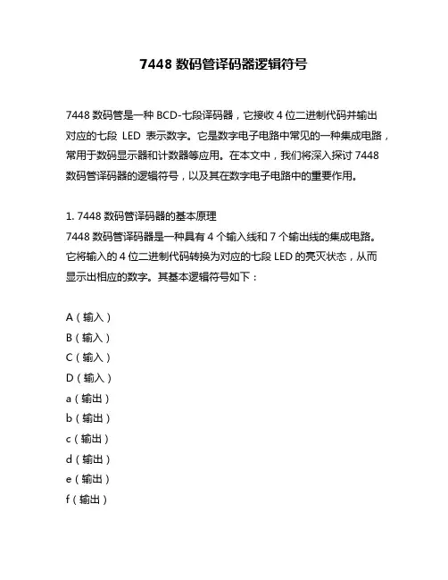
2.4 7448译码器7448是7段显示译码器,输出高电平有效的译码器。
工作电压为5V,用于驱动共阴极数码管,7448除了有实现8段显示译码器基本功能的输入(DCBA)和输出(Ya~Yg)端外,7448还引入了灯测试输入端(LT)和动态灭零输入端(RBI),以及既有输入功能又有输出功能的消隐输入/动态灭零输出(BI/RBO)端,如图2-8所示。
由7448真值表可获知7448所具有的逻辑功能如下:图2.8 7448引脚功能图(1)7段译码功能(LT=1,RBI=1)在灯测试输入端(LT)和动态灭零输入端(RBI)都接无效电平时,输入DCBA经7448译码,输出高电平有效的7段字符显示器的驱动信号,显示相应字符。
除DCBA = 0000外,RBI也可以接低电平,见表1中1~16行。
(2)消隐功能(BI=0)此时BI/RBO端作为输入端,该端输入低电平信号时,表1倒数第3行,无论LT 和RBI输入什么电平信号,不管输入DCBA为什么状态,输出全为“0”,7段显示器熄灭。
该功能主要用于多显示器的动态显示。
(3)灯测试功能(LT = 0)此时BI/RBO端作为输出端,该端输入低电平信号时,表1最后一行,与及DCBA输入无关,输出全为“1”,显示器7个字段都点亮。
该功能用于7段显示器测试,判别是否有损坏的字段。
(4)动态灭零功能(LT=1,RBI=1)此时BI/RBO端也作为输出端,LT 端输入高电平信号,RBI 端输入低电平信号,若时DCBA = 0000,表1倒数第2行,输出全为“0”,显示器熄灭,不显示这个零。
DCB A≠0,则对显示无影响。
该功能主要用于多个7段显示器同时显示时熄灭高位的零。
(5)7448/SN7448译码器0-9真值表如表2.2所示:表2.2 7448/SN7448译码器0-9真值表数码管是一种半导体发光器件,其基本单元是发光二极管。
2.5.1产品分类数码管按段数分为七段数码管和八段数码管,八段数码管比七段数码管多一个发光二极管单元(多一个小数点显示);按能显示多少个“8”可分为1位、2位、4位等等数码管。
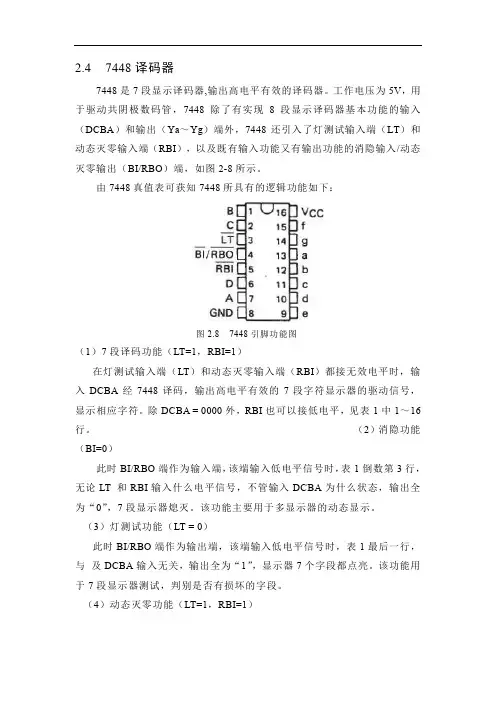
7448数码管译码器逻辑符号7448数码管译码器是一种常用的数字逻辑集成电路,它能够将二进制代码转换为七段数码管上显示的相应数字和字母字符。
这种译码器具有广泛的应用,可以在计算机、通信、仪器仪表等领域中发挥重要作用。
7448数码管译码器的输入是一个4位的二进制代码,输出是对应的七段数码管上的显示字符。
它可以译码的输入范围是从0000到1111,对应的输出范围是从0到F(十六进制)。
下面我们来详细介绍7448数码管译码器的逻辑符号和工作原理。
7448数码管译码器的逻辑符号如下所示:```___D3 -| |- VccD2 -| |D1 -| |- aD0 -| |- bCPL -| |- cPL -| |- dGND -|___|- ef```其中,D0、D1、D2和D3是译码器的输入引脚,它们对应四位二进制代码的每一位。
a、b、c、d、e、f和g是译码器的输出引脚,它们对应七段数码管的每一段。
7448数码管译码器的工作原理如下:1. 根据输入的四位二进制代码,译码器将会识别出输入所对应的数字或字母字符。
2. 根据输入代码和译码表,译码器将会输出对应的七段数码管显示字符的控制信号。
3. 根据输出的控制信号,数码管将会点亮对应的段,从而显示出相应的数字或字母字符。
7448数码管译码器内部采用了译码表来实现将输入代码转换为显示字符的功能。
下面是一个简化的译码表示例:```________|__a___ |f| |b || g | ||_____|__||__g__| |e| |c || d | ||_____|__|```译码表中的每一行代表一个十六进制数字或字母字符。
每一列代表七段数码管的一个段,其中a、b、c、d、e、f和g对应译码器的输出引脚。
通过查表的方式,译码器可以准确选择正确的输出段,从而显示出正确的数字或字母字符。
7448数码管译码器的逻辑功能是通过门电路和触发器电路实现的。
它内部包含了多个与门、多个非门和多个触发器。
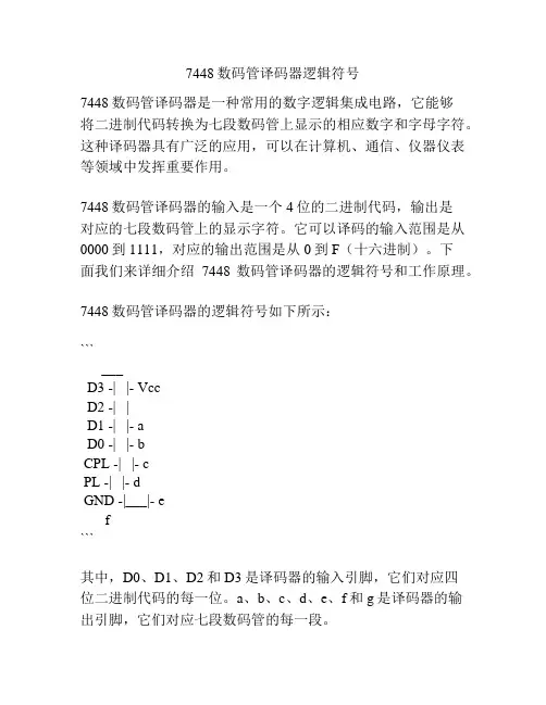
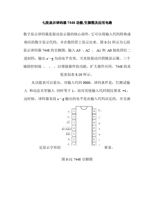
七段显示译码器7448功能,引脚图及应用电路数字显示译码器是驱动显示器的核心部件,它可以将输入代码转换成相应的数字显示代码,并在数码管上显示出来。
图8-51所示为七段显示译码器7448的引脚图,输入A3、A2、A1和A0接收四位二进制码,输出a〜g为高电平有效,可直接驱动共阴极显示器,三个辅助控制端厅、亦7|、可亦而,以增强器件的功能,扩大器件应用。
7448的真值表如表8-20所示。
从功能表可以看出,对输入代码0000,译码条件是:灯测试输入和动态灭零输入同时等于1,而对其他输入代码则仅要求=1,这时候,译码器各段a〜g输出的电平是由输入代码决定的,并且满足显示字形的要求。
图8-51 7448引脚图表8-20 7448功能表十轆数输入输出17A A A他。
住b d/s 01100u0I L11111011K00011011000021K00101110110131K D0111111100141K Q10010110011 1乂010]11011011«1011010011111710111111]0000>110001111111191*1001111110111011D1d100A1101111K101110n11001121K11D010i0D0]113111D111001011H1K111010001111151111]1D000000消隐:X00000000垃X X X K动态灭零1V00D000Q00000 0丈M艾11111111灯测试输入厅I低电平有效。
当厅=0时,无论其他输入端是什么状态,所有输出a〜g均为1,显示字形&该输入端常用于检查7448本身及显示器的好坏。
动态灭零输入亟低电平有效。
当厅=1,画川,且输入代码_ 1时,输出a〜g均为低电平,即与0000码相应的字形0 不显示,故称灭零”利用盯=1与画=0,可以实现某一位数码的消隐”时,厨亦而,其他情况下阪帀而=1。

7446/7447 数码管驱动芯片
目录
总体概述 (1)
引脚介绍 (1)
推荐使用条件 (2)
真值表 (3)
芯片应用总结: (4)
芯片应用注意事项: (5)
总体概述
7446和7447具有低电平有效输出,旨在直接驱动共阳极LED或白炽灯指示器。
芯片具有消隐功能、灭零功能以及数码管测试功能。
当输入端输入的二进制数在0-9时,可以数码管可以显示0-9,当输入端输入的二进制数在A-F时,数码管将显示不同的符号(非数字)。
芯片7446和芯片7447的基本逻辑功能相同,不同之处见“推荐使用条件”章节中表1和表2中标注红色底纹部分。
当BI/RBO节点处于高逻辑电平时,可以通过LT引脚测试数码管所有段的好坏。
芯片包含覆盖消隐输入引脚(BI),该引脚可用于控制灯强度(通过脉冲)或抑制输出。
引脚介绍
7446与7447的外观如图1所示。
该芯片共16个引脚。
其中16
1。
七段显示译码器7448功能,引脚图及应用电路数字显示译码器是驱动显示器的核心部件,它可以将输入代码转换成相应的数字显示代码,并在数码管上显示出来。
图8-51所示为七段显示译码器7448的引脚图,输入A3 、A2 、A1和A0接收四位二进制码,输出a~g为高电平有效,可直接驱动共阴极显示器,三个辅助控制端、、,以增强器件的功能,扩大器件应用。
7448的真值表如表8-20所示。
从功能表可以看出,对输入代码0000,译码条件是:灯测试输入和动态灭零输入同时等于1,而对其他输入代码则仅要求=1,这时候,译码器各段a~g输出的电平是由输入代码决定的,并且满足显示字形的要求。
图8-51 7448引脚图表8-20 7448功能表灯测试输入低电平有效。
当= 0时,无论其他输入端是什么状态,所有输出a~g均为1,显示字形8。
该输入端常用于检查7448本身及显示器的好坏。
动态灭零输入低电平有效。
当=1,,且输入代码时,输出a ~g均为低电平,即与0000码相应的字形0不显示,故称“灭零”。
利用=1与= 0,可以实现某一位数码的“消隐”。
灭灯输入/动态灭零输出是特殊控制端,既可作输入,又可作输出。
当作输入使用,且= 0时,无论其他输入端是什么电平,所有输出a~g均为0,字形熄灭。
作为输出使用时,受和控制,只有当,,且输入代码时,,其他情况下。
该端主要用于显示多位数字时多个译码器之间的连接。
【例8-13】七段显示器构成两位数字译码显示电路如图8-52所示。
当输入8421BCD码时,试分析两个显示器分别显示的数码范围。
图8-52 两位数字译码显示电路解:图8-52所示的电路中,两片7448的均接高电平。
由于7448(1)的,所以,当它的输入代码为0000时,满足灭零条件,显示器(1)无字形显示。
7448(2)的,所以,当它的输入代码为0000时,仍能正常显示,显示器(2)显示0。
而对其他输入代码,由于,译码器都可以输出相应的电平驱动显示器。
![数码管简介[推荐阅读]](https://uimg.taocdn.com/1c94560cae45b307e87101f69e3143323868f578.webp)
数码管简介[推荐阅读]第一篇:数码管简介(注:此文档内容均复制:数码管_百科名片,仅供下载方便。
)数码管百科名片数码管是一种半导体发光器件,其基本单元是发光二极管。
一产品分类数码管按段数分为七段数码管和八段数码管,八段数码管比七段数码管多一个发光二极管单元(多一个小数点显示);按能显示多少个“8”可分为1位、2位、4位等等数码管。
按发光二极管单元连接方式分为共阳极数码管和共阴极数码管。
共阳数码管是指将所有发光二极管的阳极接到一起形成公共阳极(COM)的数码管。
共阳数码管在应用时应将公共极COM接到+5V,当某一字段发光二极管的阴极为低电平时,相应字段就点亮。
当某一字段的阴极为高电平时,相应字段就不亮。
共阴数码管是指将所有发光二极管的阴极接到一起形成公共阴极(COM)的数码管。
共阴数码管在应用时应将公共极COM接到地线GND上,当某一字段发光二极管的阳极为高电平时,相应字段就点亮。
当某一字段的阳极为低电平时,相应字段就不亮。
二驱动方式数码管要正常显示,就要用驱动电路来驱动数码管的各个段码,从而显示出我们要的数字,因此根据数码管的驱动方式的不同,可以分为静态式和动态式两类。
1)静态显示驱动的I/O端口进行驱动,或者使用如BCD码二-十进制译码器译码进行驱动。
静态驱动的优点是编程简单,显示亮度高,缺点是占用I/O端口多,如驱动5个数码管静态显示则需要5×8=40根I/O端口来驱动,要知道一个89S51单片机可用的I/O端口才32个呢:),实际应用时必须增加译码驱动器进行驱动,增加了硬件电路的复杂性。
2)动态显示驱动数码管动态显示接口是单片机中应用最为广泛的一种显示方式之一,动态驱动是将所有数码管的8个显示笔划“a,b,c,d,e,f,g,dp”的同名端连在一起,另外为每个数码管的公共极COM增加位选通控制电路,位选通由各自独立的I/O线控制,当单片机输出字形码时,所有数码管都接收到相同的字形码,但究竟是那个数码管会显示出字形,取决于单片机对位选通COM端电路的控制,所以我们只要将需要显示的数码管的选通控制打开,该位就显示出字形,没有选通的数码管就不会亮。
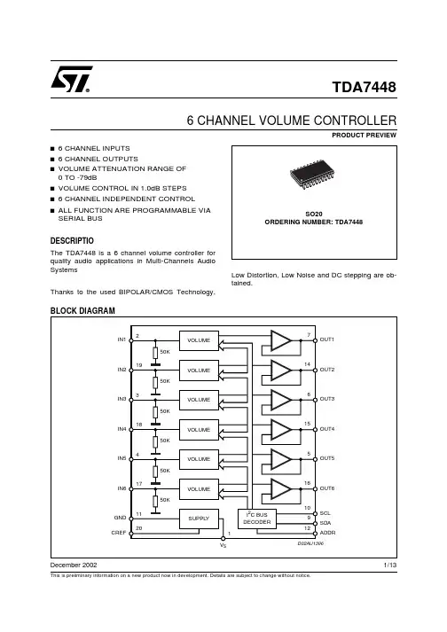
1/13TDA7448December 2002This is preliminary information on a new product now in development. Details are subject to change without notice.s 6 CHANNEL INPUTS s 6 CHANNEL OUTPUTSs VOLUME ATTENUATION RANGE OF 0 TO -79dBs VOLUME CONTROL IN 1.0dB STEPS s 6 CHANNEL INDEPENDENT CONTROL sALL FUNCTION ARE PROGRAMMABLE VIA SERIAL BUSDESCRIPTIOThe TDA7448 is a 6 channel volume controller for quality audio applications in Multi-Channels Audio SystemsThanks to the used BIPOLAR/CMOS Technology,Low Distortion, Low Noise and DC stepping are ob-tained.PRODUCT PREVIEW6 CHANNEL VOLUME CONTROLLERTDA7448ABSOLUTE MAXIMUM RATINGSSymbol Parameter Value Unit V S Operating Supply Voltage10.5V T amb Operating Ambient Temperature-10 to 85°C T stg Storage Temperature Range-55 to 150°CTHERMAL DATASymbol Parameter Value Unit R th j-pin thermal Resistance junction-pins150°C/WQUICK REFERENCE DATASymbol Parameter Min.Typ.Max.Unit V S Supply Voltage 4.75910V V CL Max Input Signal Handling2Vrms THD Total Harmonic Distortion V = 1Vrms f =1KHz0.010.1% S/N Signal to Noise Ratio Vout = 1Vrms100dB S C Channel Separation f = 1KHz90dB Volume Control (1dB step)-790dBMute Attenuation90dB 2/13TDA7448 ELECTRICAL CHARACTERISTCS(refer to the test circuit T amb = 25°C, V S = 9V, R L = 10KΩ, R G = 600Ω, unless otherwise specified)Symbol Parameter Test Condition Min. Typ.Max.Unit SUPPLYV S Supply Voltage 4.75910VI S Supply Current7mASVR Ripple Rejection80dB INPUT STAGER IN Input Resistance355065KΩV CL Clipping Level THD = 0.3%2 2.5Vrms S IN Input Separation The selected input is grounded90dBthrough a 2.2µ capacitorVOLUME CONTROLC RANGE Control Range79dBA VMAX Max. Attenuation79dBA STEP Step Resolution0.51 1.5dBE A Attenuation Set Error A V = 0 to -24dB-101dBA V = -24 to -79dB-2.00 2.0dBE T Tracking Error A V = 0 to -24dB-101dBA V = -24 to -79dB-202dBV DC DC Step adyacent attenuation steps-303mVA mute Mute Attenuation90db AUDIO OUTPUTSV CLIP Clipping Level THD = 0.3%2 2.5Vrms R L Output Load Resistance2KΩV DC DC Voltage Level 4.5V GENERAL1015µVE NO Output Noise BW = 20Hz to 20KHzAll gains = 0dB, FlatS/N Signal to Noise Ratio All gains = 0dB; V O = 1Vrms100dB S C Channel Separation left/Right8090dB THD Distortion A V = 0; V I = 1Vrms0.010.1% BUS INPUTV Il Input Low Voltage1V V IH Input High Voltage 2.5VI IN Input Current V IN = 0.4V-55µAV O Output Voltage SDAI O = 1.6mA0.40.8VAchnowledge3/13TDA74484/13Figure 1. Test circuitAPPLICATION SUGGESTIONSThe volume control range is 0 to -79dB, by 1dB step resolution.The very high resolution allows the implementation of systems free from any noise acoustical effect.CREFThe suggested 10µF reference capacitor (CREF)value can be reduced to 4.7µF if the application re-quires faster power ON.Figure 2. THD vs. frequencyFigure 3. THD vs. R LOADFigure 4. Channel separation vs. frequencyTDA7448I2C BUS INTERFACEData transmission from microprocessor to the TDA7448 and vice versa takes place through the 2 wires I2C BUS in-terface, consisting of the two lines SDA and SCL (pull-up resistors to positive supply voltage must be connected).Data ValidityAs shown in fig. 1, the data on the SDA line must be stable during the high period of the clock. The HIGH and LOW state of the data line can only change when the clock signal on the SCL line is LOW.Start and Stop ConditionsAs shown in fig. 2 a start condition is a HIGH to LOW transition of the SDA line while SCL is HIGH. The stop condition is a LOW to HIGH transition of the SDA line while SCL is HIGH.Byte FormatEvery byte transferred on the SDA line must contain 8 bits. Each byte must be followed by an acknowledge bit. The MSB is transferred first.AcknowledgeThe master (µP) puts a resistive HIGH level on the SDA line during the acknowledge clock pulse (see fig. 5). The peripheral (audio processor) that acknowledges has to pull-down (LOW) the SDA line during this clock pulse.The audio processor which has been addressed has to generate an acknowledge after the reception of each byte, otherwise the SDA line remains at the HIGH level during the ninth clock pulse time. In this case the master transmitter can generate the STOP information in order to abort the transfer.Transmission without AcknowledgeAvoiding to detect the acknowledge of the audio processor, the µP can use a simpler transmission: simply it waits one clock without checking the slave acknowledging, and sends the new data.This approach of course is less protected from misworking.2225/13TDA74486/13SOFTWARE SPECIFICATION Interface ProtocolThe interface protocol comprises:s A start condition (S)s A chip address byte, containing the TDA7448 address s A subaddress bytess A sequence of data (N byte + acknowledge)sA stop condition (P))ACK = Acknowledge;S = Start;P = Stop; A = Address; B = Auto IncrementEXAMPLESNo Incremental BusThe TDA7448 receives a start condition, the correct chip address, a subaddress with the B = 0 (no incremental bus), N-data (all these data concern the subaddress selected), a stop condition.Incremental BusThe TDA7448 receivea start conditions, the correct chip address, a subaddress with the B = 1 (incremental bus):now it is in a loop condition with an autoincrease of the subaddress whereas SUBADDRESS from "XXX1000"to "XXX1111" of DATA are ignored.The DATA 1 concern the subaddress sent, and the DATA 2 concern the subaddress sent plus one in the loop etc, and at the end it receivers the stop condition.DATA BYTESAddress= 88 (HEX) (10001000): ADDR open; 8A (HEX) (10001010): connect to supply FUNCTION SELECTION: subaddressB=1: INCREMENTAL BUS; ACTIVE B=0: NO INCREMENTAL BUS X= DON’T CAREMSB LSB SUBADDRESSD7D6D5D4D3D2D1D0X X X B 0000SPEAKER A TTENUATION OUT 1X X X B 0001SPEAKER A TTENUATION OUT 2X X X B 0010SPEAKER ATTENUATION OUT 3X X X B 0011SPEAKER A TTENUATION OUT 4X X X B 0100SPEAKER A TTENUATION OUT 5X X X B 0101SPEAKER A TTENUATION OUT 6X X X B 0110NOT USED”XXXB111NOT USEDTDA7448 In Incremental Bus Mode, the three “not used” functions must be addressed in any case. For example to refresh “ Speaker Attenuation 3 = 0dB and Speaker Attenuation 6 = -40 dB”; the following bytes must be sent:SUBADDRESS XXX10010SPEAKER A TTENUATION OUT 1XXXXXXXXSPEAKER A TTENUATION OUT 2XXXXXXXXSPEAKER A TTENUATION OUT 300000000SPEAKER A TTENUATION OUT 4XXXXXXXXSPEAKER A TTENUATION OUT 5XXXXXXXXSPEAKER A TTENUATION OUT 600101111SPEAKER ATTENUATION SELECTIONMSB LSBSPEAKER ATTENUATION D7D6D5D4D3D2D1D00000dB001-1dB010-2dB011-3dB100-4dB101-5dB110-6dB111-7dB00000-0dB00001-8dB00010-16dB00011-24dB00100-32dB00101-40dB00110-48dB00111-56dB01-64dB10-72dB11MUTEvalue = 0 to -79dB and MUTE7/13TDA74488/13Figure 8. PIN:20Figure 9. PINS: 5, 6, 7, 14, 15, 16Figure 10. PINS: 2, 3, 4, 17, 18, 19Figure 11. PINS: 10Figure 12. PINS: 9TDA7448 Figure 13. Test and Application Circuit9/13TDA744810/13Figure 14. Component Layout (65 x 72mm)Figure 15. PC Board (Component side)TDA7448 Figure 16. PC Board (Solder side)11/1312/13Information furnished is believed to be accurate and reliable. However, STMicroelectronics assumes no responsibility for the consequences of use of such information nor for any infringement of patents or other rights of third parties which may result from its use. No license is granted by implication or otherwise under any patent or patent rights of STMicroelectronics. Specifications mentioned in this publication are subject to change without notice. This publication supersedes and replaces all information previously supplied. STMicroelectronics products are not authorized for use as critical components in life support devices or systems without express written approval of STMicroelectronics.The ST logo is a registered trademark of STMicroelectronics©2002 STMicroelectronics - All Rights ReservedSTMicroelectronics GROUP OF COMPANIESAustralia - Brazil - Canada - China - Finland - France - Germany - Hong Kong - India - Israel - Italy - Japan -Malaysia - Malta - Morocco - Singapore - Spain - Sweden - Switzerland - United Kingdom - United States.13/13。
7段数码管驱动电路芯片
驱动7段数码管的电路通常使用集成电路芯片来实现。
其中比较常见的芯片包括7447、7448、4511等。
这些芯片能够有效地控制7段数码管的显示,简化了数字显示电路的设计和实现。
首先,我们来看一下7447芯片。
这是一种BCD-7段数码管译码器,能够将BCD码转换为7段数码管的控制信号。
它可以直接驱动共阳极的数码管,通过输入BCD码,输出对应的控制信号,从而实现数字的显示。
除了7447之外,还有7448芯片,它与7447类似,也是BCD-7段数码管译码器,但输出极性与7447相反,可以直接驱动共阴极的数码管。
另外,4511芯片是一种BCD-7段数码管译码驱动器,它可以直接将BCD码转换为7段数码管的控制信号,并且具有存储器功能,能够存储上一次的输入状态,适合用于静态显示。
这些芯片通常需要外部电路的支持,例如输入BCD码的开关电路、时钟信号的产生电路等。
在使用这些芯片的时候,需要注意输
入端的电平和输入信号的稳定性,以确保数字显示的准确性和稳定性。
另外,还有一些基于微控制器或FPGA的数字驱动方案,它们能够更加灵活地实现数字显示,但相对而言也更加复杂。
总的来说,选择合适的驱动芯片取决于具体的应用需求和设计考虑。
A +_7448简易编程:FC-7448报警主机的编程并是很不复杂。
在编程之前,敬请用户必须先详细地阅读安装使用说明书,并清楚的知道你所需要的功能,根据所需列出编程表,这样方便于编程。
编程前请认真阅读说明书,正确的接好连线。
(正确接好连线是编好程序的前提)。
如果是第一次使用FC-7448主机,在编程完成前,建议安装技术人员不要将探测器接入主机,只需要将线尾电阻和扩展模块接在主上就可以,将主机调试好后,在将探测器接入防区,这样如果系统有故障,有利于工程技术人员判断是主机系统故障还是探测器故障。
一、正常布防:密码(1234)+“布防”键。
二、撤防和消警:密码(1234)+“撤防”键。
三、强制布防:密码(1234)+“布防”键+“旁路”键四、防区旁路:密码(1234)+“旁路”键+XXX(防区号,且一定是三位数,如008)五、进入编程和退出编程:进入编程是9876#0(密码+#0),退出编程是按“*”四秒钟,听到“嘀”一声表示已退出编程。
六、如何填写数据:FC-7448主机的编程地址一定是四位数,地址的数据一定是两位数。
进入编程后,键盘的灯都会闪动,LCD显示:Prog Mode 4.05 Adr= Adr=后面的就是要写上去的四位数的地址。
输入地址后,接着输入21# 则会交替显示该地址上的两位数据;或者按“#”则可以出现数据1;再按“#”则可出现数据2。
(出厂值,可以通过编程改变的),然后自动跳到下一个地址。
如果需要对某些地址编程,则需连续按两次“*”则可以回到Prog Mode 4.05 Adr= 。
七、确定防区的功能:(地址是0001—0030),所谓防区功能就是该防区是延时防区、即时防区、24小时防区等等。
其中01代表延时防区;03代表周界即时防区;06代表内部即时防区;07代表24小时防区。
(此项一般不用编写,用出厂值即可)八、确定一个防区的功能:(地址是0031—0278),0031代表第一防区,0032代表第二防区,如此类推………如果想把第八防区设定为24小时防区,即可以把地址0038中的数据改为07 ,再按“#”确认就可以了。
7448 升压电阻7448升压电阻是一种常见的电子元件,主要用于电路中的升压转换。
它的作用是将输入电压升高到所需的输出电压,以满足电路的工作要求。
本文将从工作原理、特性以及应用方面来介绍7448升压电阻。
一、工作原理7448升压电阻是一种电阻器,其工作原理基于电阻器的特性。
电阻器是电路中常用的被动元件,通过阻碍电流流动来实现电阻的作用。
升压电阻的工作原理是在电路中串联一个电阻,通过电阻的阻值来控制电压的升高。
二、特性1. 阻值:7448升压电阻的阻值通常为固定值,常见的有100欧姆、200欧姆等。
阻值的选择要根据电路的需求来确定,以保证电路能够正常工作。
2. 额定功率:7448升压电阻的额定功率是指电阻器能够承受的最大功率。
在选择电阻器时,要根据电路的功率要求来确定,以避免电阻器过载而损坏。
3. 精度:7448升压电阻的精度通常为5%或10%。
精度越高,电阻器的阻值与标称值的偏差越小,电路的稳定性越高。
4. 温度系数:7448升压电阻的温度系数是指电阻值随温度变化的程度。
温度系数越小,电阻器的阻值稳定性越好。
三、应用7448升压电阻在电子领域有广泛的应用,下面列举几个常见的应用场景:1. 电源升压:在某些电子设备中,需要将输入电源的电压升高到所需的工作电压才能正常工作。
此时可以使用7448升压电阻来实现电压的升高。
2. 信号处理:在某些信号处理电路中,为了提高信号的质量和稳定性,需要对信号进行升压处理。
7448升压电阻可以提供所需的升压功能。
3. LED驱动:在LED照明领域,为了使LED正常工作,需要提供适当的电压和电流。
7448升压电阻可以用来升高输入电压,以满足LED的工作要求。
7448升压电阻是一种常见的电子元件,通过控制阻值来实现电压的升高。
它具有固定的阻值、额定功率、精度和温度系数等特性。
在电源升压、信号处理和LED驱动等应用中有着广泛的应用。
了解7448升压电阻的工作原理和特性,对于电子工程师和电路设计者来说是非常重要的。
实验三译码显示电路实验三译码显示电路译码显示电路是由多个数字输入端口和一个显示端口构成的数字电路。
该电路将数字输入信号转换为相应的字形或字符形式,并通过显示端口输出,是数字系统中非常重要的部分。
本实验将学习到译码显示电路的基本原理、组成要素、设计方法以及实际应用。
下面将从以下几个方面进行详细的介绍:一、数码管的原理数码管是数字电路中最常见的数字输出设备之一,它是使用半导体技术制成的一种电子元件。
数码管通常由8个发光二极管(LED)组成,每个发光二极管对应一个数字位,它们可以组合成不同的数字和字母字符以显示在屏幕上。
数码管按照共阳和共阴两种方式区分,其中共阳数码管的阳极连接在信号源上,共阴数码管的阴极连接在信号源上。
二、二进制代码在数字系统中,数字信息通常使用二进制代码进行表示和存储。
二进制代码是由二个符号“0”和“1”组成的数字系统。
它利用位权值原理表示数字大小,其中位权从右往左每增加一位,权重就翻倍。
例如,一个8位的二进制代码可以表示0~255之间的任意数字。
三、译码芯片译码芯片是一种数字电路芯片,它能够将输入的二进制信号转换为对应的字符或数字形式,并通过数码管进行显示。
常见的译码芯片有7447、7448、74148等。
其中,7447是一个4位二进制-7段数码管译码器芯片,7448是一个BCD-7段数码管译码器芯片,74148是一个8位二进制-3线-8线译码器芯片。
这些译码芯片的功能相似,但使用的方式略有不同,需要根据实际情况进行选择。
四、译码显示电路的设计译码显示电路的设计可以分为两个主要步骤:电路分析和电路设计。
电路分析包括对数字信号或数字代码的分析、对数码管和译码芯片等元件的分析,制定电路图和逻辑关系等步骤;电路设计则包括对电路图细节的调整、对元件的选择和连接方式的确定,以及对电路的测试和调试。
在进行电路设计时,还需要考虑电路的功耗、稳定性和可靠性等因素。
五、译码显示电路的应用译码显示电路广泛应用于各种数字系统中,如计算机、计算器、智能卡、微控制器等。
工作电压5V常用的BCD 对七段显示器译码器/驱动器之IC 包装计有TTL 之7446、7447、7448、7449 与CMOS 之4511 等等。
其中7446、7447 必须使用共阳极七段显示器,7448、7449、4511等则使用共阴极七段显示器。
中文资料838电子图1为7447集成电路译码器之引脚图与真值表如表1。
在正常操作时,当输入DCBA=0010 则输出abcdefg=0010010。
故使显示器显示"2"。
当输入DCBA=0110 时,输出abcdeg=1100000,显示器显示"6"。
在7447 中尚有LT、RBI 与BI/RBO 之控制脚,其功能分述如下:该电路是由与非门、输入缓冲器和7 个与或非门组成的BCD-7 段译码器/驱动器。
通常是低电平有效,高的灌入电流的输出可直接驱动显示器。
7 个与非门和一个驱动器成对连接,以产生可用的BCD 数据及其补码至7 个与或非译码门。
剩下的与非门和3 个输入缓冲器作为试灯输入(LT)端、灭灯输入/动态灭灯输出(BI/RBO)端及动态灭灯输入(RBI )端。
该电路接受4 位二进制编码—十进制数(BCD)输入并借助于辅助输入端状态将输入数据译码后去驱动一个七段显示器。
输出结构设计成能承受7 段显示所需要的相当高的电压。
驱动显示器各段所需的高达24mA 的电流可以由其高性能的输出晶体管来直接提供。
BCD 输入计数9 以上的显示图案是鉴定输入条件的唯一信号。
该电路有自动前、后沿灭零控制(RBI和RBO)。
试灯(LT)可在端处在高电平的任何时刻去进行,该电路还含有一个灭灯输入(BI),它用来控制灯的亮度或禁止输出。
该电路在应用中可以驱动共阳极的发光二极管或直接驱动白炽灯指示器。
838电子7447 之输出系为驱动器设计,其逻辑0 之吸入电流高达40mA,故在使用必须加入330Ω 左右电阻加以限流,以免过大电流流经LED 而烧毁显示器,如图3 所示。
硬件电路开发中数码管常用知识数码管简介数码管是一种半导体发光器件,其基本单元是发光二极管。
数码管按段数可分为七段数码管和八段数码管,八段数码管比七段数码管多一个发光二极管单元,也就是多一个小数点(DP),这个小数点可以更精确的表示数码管想要显示的内容。
按能显示多少个(8)可分为1位、2位、3位、4位、5位、6位、7位等数码管。
七段数码管八段数码管3位、4位、6位数码管数码管内部结构LED数码管(LED Segment Displays)是由多个发光二极管封装在一起组成“8”字型的器件,引线已在内部连接完成,只需引出它们的各个笔划,公共电极。
LED数码管常用段数一般为7段,有的另加一个小数点。
LED 数码管根据接法不同分为共阴和共阳两类。
了解LED 的这些特性,对编程是很重要的,因为不同类型的数码管,除了它们的硬件电路有差异外,编程方法也是不同的。
下图是共阴和共阳极数码管的内部电路,它们的发光原理是一样的,只是它们的电源极性不同而已。
数码管内部结构数码管的类型由发光二极管按照一定排列封装在一起,七个发光二极管组成8字形。
二极管之间引线集成在数码管内部,引出数码管外部的是各个笔划和公共电极。
这些发光二极管分别由字母a ,b ,c ,d ,e ,f ,g 来表示。
通过选择数码管上的发光二极管发光的搭配来显示字符。
这种数码管称为七段数码管。
八段数码管比七段数码管多一个发光二极管单元(多一个小数点显示)。
按数码管内部发光二极管单元连接方式,可以分为共阳极数码管和共阴极数码管。
1、共阳极数码管:是指将所有发光二极管阳极接到一起形成公共阳极。
共阳数码管在应用时应将公共极接到+5V,当某一字段发光二极管的阴极为低电平时,相应字段就点亮。
当某一字段的阴极为高电平时,相应字段就不亮。
2、共阴极数码管:是指将所有发光二极管的阴极接到一起形成公共阴极。
共阴数码管在应用时应将公共极接到地线GND上,当某一字段发光二极管的阳极为高电平时,相应字段就点亮。
Freescale SemiconductorTechnical DataThis document is primarily concerned with the MPC7448, which is targeted at networking and computing systems applications. This document describes pertinent electrical and physical characteristics of the MPC7448. For information regarding specific MPC7448 part numbers covered by this document and part numbers covered by other documents, refer to Section11, “Part Numbering and Marking.” For functional characteristics of the processor, refer to the MPC7450 RISC Microprocessor Family Reference Manual.To locate any published updates for this document, refer to the website listed on the back cover of this document.1OverviewThe MPC7448 is the sixth implementation of fourth-generation(G4) microprocessors from Freescale. TheMPC7448, built on Power Architecture™ technology, implements the PowerPC™ instruction set architecture version 1.0 and is targeted at networking and computing systems applications. The MPC7448 consists of a processor core and a 1-Mbyte L2.Figure1 shows a block diagram of the MPC7448. The core is a high-performance superscalar design supporting adouble-precision floating-point unit and a SIMD multimedia unit. The memory storage subsystem supports the MPX bus protocol and a subset of the 60x bus protocol to main memory and other system resources.Document Number:MPC7448ECRev. 4, 3/2007Contents1.Overview . . . . . . . . . . . . . . . . . . . . . . . . . . . . . . . . . . . 12.Features . . . . . . . . . . . . . . . . . . . . . . . . . . . . . . . . . . . . 3parison with the MPC7447A, MPC7447,MPC7445, and MPC7441 . . . . . . . . . . . . . . . . . . . . . . 74.General Parameters . . . . . . . . . . . . . . . . . . . . . . . . . . . 95.Electrical and Thermal Characteristics . . . . . . . . . . . . 96.Pin Assignments . . . . . . . . . . . . . . . . . . . . . . . . . . . . 247.Pinout Listings . . . . . . . . . . . . . . . . . . . . . . . . . . . . . 258.Package Description . . . . . . . . . . . . . . . . . . . . . . . . . 299.System Design Information . . . . . . . . . . . . . . . . . . . 3510.Document Revision History . . . . . . . . . . . . . . . . . . . 5511.Part Numbering and Marking . . . . . . . . . . . . . . . . . . 57MPC7448RISC MicroprocessorHardware Specifications 元器件交易网元器件交易网OverviewFigure1. MPC7448 Block DiagramFeatures2FeaturesThis section summarizes features of the MPC7448 implementation.Major features of the MPC7448 are as follows:•High-performance, superscalar microprocessor—Up to four instructions can be fetched from the instruction cache at a time.—Up to three instructions plus a branch instruction can be dispatched to the issue queues at a time.—Up to 12 instructions can be in the instruction queue (IQ).—Up to 16 instructions can be at some stage of execution simultaneously.—Single-cycle execution for most instructions—One instruction per clock cycle throughput for most instructions—Seven-stage pipeline control•Eleven independent execution units and three register files—Branch processing unit (BPU) features static and dynamic branch prediction–128-entry (32-set, four-way set-associative) branch target instruction cache (BTIC), a cache of branch instructions that have been encountered in branch/loop code sequences. If a targetinstruction is in the BTIC, it is fetched into the instruction queue a cycle sooner than it canbe made available from the instruction cache. Typically, a fetch that hits the BTIC providesthe first four instructions in the target stream.–2048-entry branch history table (BHT) with 2 bits per entry for four levels ofprediction—not taken, strongly not taken, taken, and strongly taken–Up to three outstanding speculative branches–Branch instructions that do not update the count register (CTR) or link register (LR) are often removed from the instruction stream.–Eight-entry link register stack to predict the target address of Branch Conditional to Link Register (bclr) instructions—Four integer units (IUs) that share 32 GPRs for integer operands–Three identical IUs (IU1a, IU1b, and IU1c) can execute all integer instructions except multiply, divide, and move to/from special-purpose register instructions.–IU2 executes miscellaneous instructions, including the CR logical operations, integer multiplication and division instructions, and move to/from special-purpose registerinstructions.—Five-stage FPU and 32-entry FPR file–Fully IEEE Std. 754™-1985–compliant FPU for both single- and double-precision operations–Supports non-IEEE mode for time-critical operations–Hardware support for denormalized numbers–Thirty-two 64-bit FPRs for single- or double-precision operandsFeatures—Four vector units and 32-entry vector register file (VRs)–V ector permute unit (VPU)–V ector integer unit 1 (VIU1) handles short-latency AltiV ec™ integer instructions, such as vector add instructions (for example, vaddsbs, vaddshs, and vaddsws).–V ector integer unit 2 (VIU2) handles longer-latency AltiVec integer instructions, such as vector multiply add instructions (for example, vmhaddshs, vmhraddshs,andvmladduhm).–V ector floating-point unit (VFPU)—Three-stage load/store unit (LSU)–Supports integer, floating-point, and vector instruction load/store traffic–Four-entry vector touch queue (VTQ) supports all four architected AltiV ec data stream operations–Three-cycle GPR and AltiVec load latency (byte, half word, word, vector) with one-cycle throughput–Four-cycle FPR load latency (single, double) with one-cycle throughput–No additional delay for misaligned access within double-word boundary– A dedicated adder calculates effective addresses (EAs).–Supports store gathering–Performs alignment, normalization, and precision conversion for floating-point data–Executes cache control and TLB instructions–Performs alignment, zero padding, and sign extension for integer data–Supports hits under misses (multiple outstanding misses)–Supports both big- and little-endian modes, including misaligned little-endian accesses •Three issue queues, FIQ, VIQ, and GIQ, can accept as many as one, two, and three instructions, respectively, in a cycle. Instruction dispatch requires the following:—Instructions can only be dispatched from the three lowest IQ entries—IQ0, IQ1, and IQ2.—A maximum of three instructions can be dispatched to the issue queues per clock cycle.—Space must be available in the CQ for an instruction to dispatch (this includes instructions that are assigned a space in the CQ but not in an issue queue).•Rename buffers—16 GPR rename buffers—16 FPR rename buffers—16 VR rename buffers•Dispatch unit—Decode/dispatch stage fully decodes each instruction•Completion unit—Retires an instruction from the 16-entry completion queue (CQ) when all instructions ahead of it have been completed, the instruction has finished executing, and no exceptions are pending —Guarantees sequential programming model (precise exception model)Features—Monitors all dispatched instructions and retires them in order—Tracks unresolved branches and flushes instructions after a mispredicted branch—Retires as many as three instructions per clock cycle•Separate on-chip L1 instruction and data caches (Harvard architecture)—32-Kbyte, eight-way set-associative instruction and data caches—Pseudo least-recently-used (PLRU) replacement algorithm—32-byte (eight-word) L1 cache block—Physically indexed/physical tags—Cache write-back or write-through operation programmable on a per-page or per-block basis —Instruction cache can provide four instructions per clock cycle; data cache can provide four words per clock cycle—Caches can be disabled in software.—Caches can be locked in software.—MESI data cache coherency maintained in hardware—Separate copy of data cache tags for efficient snooping—Parity support on cache—No snooping of instruction cache except for icbi instruction—Data cache supports AltiVec LRU and transient instructions—Critical double- and/or quad-word forwarding is performed as needed. Critical quad-word forwarding is used for AltiV ec loads and instruction fetches. Other accesses use criticaldouble-word forwarding.•Level 2 (L2) cache interface—On-chip, 1-Mbyte, eight-way set-associative unified instruction and data cache—Cache write-back or write-through operation programmable on a per-page or per-block basis —Parity support on cache tags—ECC or parity support on data—Error injection allows testing of error recovery software•Separate memory management units (MMUs) for instructions and data—52-bit virtual address, 32- or 36-bit physical address—Address translation for 4-Kbyte pages, variable-sized blocks, and 256-Mbyte segments—Memory programmable as write-back/write-through, caching-inhibited/caching-allowed, and memory coherency enforced/memory coherency not enforced on a page or block basis —Separate IBATs and DBA Ts (eight each) also defined as SPRs—Separate instruction and data translation lookaside buffers (TLBs)–Both TLBs are 128-entry, two-way set-associative and use an LRU replacement algorithm.–TLBs are hardware- or software-reloadable (that is, a page table search is performed in hardware or by system software on a TLB miss).Features•Efficient data flow—Although the VR/LSU interface is 128 bits, the L1/L2 bus interface allows up to 256 bits.—The L1 data cache is fully pipelined to provide 128 bits/cycle to or from the VRs.—The L2 cache is fully pipelined to provide 32 bytes per clock every other cycle to the L1 caches.—As many as 16 out-of-order transactions can be present on the MPX bus.—Store merging for multiple store misses to the same line. Only coherency action taken (address-only) for store misses merged to all 32 bytes of a cache block (no data tenure needed).—Three-entry finished store queue and five-entry completed store queue between the LSU and the L1 data cache—Separate additional queues for efficient buffering of outbound data (such as castouts and write-through stores) from the L1 data cache and L2 cache•Multiprocessing support features include the following:—Hardware-enforced, MESI cache coherency protocols for data cache—Load/store with reservation instruction pair for atomic memory references, semaphores, and other multiprocessor operations•Power and thermal management—Dynamic frequency switching (DFS) feature allows processor core frequency to be halved or quartered through software to reduce power consumption.—The following three power-saving modes are available to the system:–Nap—Instruction fetching is halted. Only the clocks for the time base, decrementer, and JTAG logic remain running. The part goes into the doze state to snoop memory operationson the bus and then back to nap using a QREQ/QACK processor-system handshakeprotocol.–Sleep—Power consumption is further reduced by disabling bus snooping, leaving only the PLL in a locked and running state. All internal functional units are disabled.–Deep sleep—When the part is in the sleep state, the system can disable the PLL. The system can then disable the SYSCLK source for greater system power savings. Power-on resetprocedures for restarting and relocking the PLL must be followed upon exiting the deepsleep state.—Instruction cache throttling provides control of instruction fetching to limit device temperature.—A new temperature diode that can determine the temperature of the microprocessor •Performance monitor can be used to help debug system designs and improve software efficiency.•In-system testability and debugging features through JTAG boundary-scan capability•Testability—LSSD scan design—IEEE Std. 1149.1™ JTAG interfaceComparison with the MPC7447A, MPC7447, MPC7445, and MPC7441•Reliability and serviceability—Parity checking on system bus—Parity checking on the L1 caches and L2 data tags—ECC or parity checking on L2 data3Comparison with the MPC7447A, MPC7447, MPC7445, and MPC7441Table1 compares the key features of the MPC7448 with the key features of the earlier MPC7447A, MPC7447, MPC7445, and MPC7441. All are based on the MPC7450 RISC microprocessor and are architecturally very similar. The MPC7448 is identical to the MPC7447A, but the MPC7448 supports 1 Mbyte of L2 cache with ECC and the use of dynamic frequency switching (DFS) with more bus-to-core ratios.Table1. Microarchitecture ComparisonMicroarchitectural Specs MPC7448MPC7447A MPC7447MPC7445MPC7441Basic Pipeline FunctionsLogic inversions per cycle18Pipeline stages up to execute5Total pipeline stages (minimum)7Pipeline maximum instruction throughput 3 + branchPipeline ResourcesInstruction buffer size12Completion buffer size16Renames (integer, float, vector)16, 16, 16Maximum Execution ThroughputSFX3Vector 2 (any 2 of 4 units)Scalar floating-point1Out-of-Order Window Size in Execution QueuesSFX integer units 1 entry × 3 queuesVector units In order, 4 queuesScalar floating-point unit In orderBranch Processing ResourcesPrediction structures BTIC, BHT, link stackBTIC size, associativity128-entry, 4-wayBHT size2K-entryLink stack depth8Unresolved branches supported3Branch taken penalty (BTIC hit)1Minimum misprediction penalty6Comparison with the MPC7447A, MPC7447, MPC7445, and MPC7441Execution Unit Timings (Latency-Throughput)Aligned load (integer, float, vector)3-1, 4-1, 3-1Misaligned load (integer, float, vector)4-2, 5-2, 4-2L1 miss, L2 hit latency with ECC (data/instruction) 12/16—L1 miss, L2 hit latency without ECC (data/instruction)11/159/13SFX (add, sub, shift, rot, cmp, logicals)1-1Integer multiply (32 × 8, 32 × 16, 32 × 32)4-1, 4-1, 5-2Scalar float5-1VSFX (vector simple)1-1VCFX (vector complex)4-1VFPU (vector float)4-1VPER (vector permute)2-1MMUsTLBs (instruction and data)128-entry, 2-way Tablewalk mechanism Hardware + softwareInstruction BA Ts/data BA Ts8/88/88/88/84/4L1 I Cache/D Cache FeaturesSize 32K/32K Associativity 8-way Locking granularity Way Parity on I cache Word Parity on D cacheByteNumber of D cache misses (load/store)5/25/1Data stream touch engines4 streamsOn-Chip Cache FeaturesCache level L2Size/associativity 1-Mbyte/8-way512-Kbyte/8-way256-Kbyte/8-wayAccess width256 bitsNumber of 32-byte sectors/line 22Parity tag Byte Byte Parity data Byte Byte Data ECC64-bit—Thermal ControlDynamic frequency switching divide-by-two mode Y es Y es No No No Dynamic frequency switching divide-by-four mode Y es No No No No Thermal diodeY esY esNoNoNoTable 1. Microarchitecture Comparison (continued)Microarchitectural SpecsMPC7448MPC7447A MPC7447MPC7445MPC7441General Parameters4General ParametersThe following list summarizes the general parameters of the MPC7448:Technology 90 nm CMOS SOI, nine-layer metal Die size8.0mm × 7.3mm Transistor count 90 millionLogic design Mixed static and dynamicPackagesSurface mount 360 ceramic ball grid array (HCTE)Surface mount 360 ceramic land grid array (HCTE)Surface mount 360 ceramic ball grid array with lead-free spheres (HCTE)Core power supply1.30 V (1700 MHz device)1.25 V (1600 MHz device)1.20 V (1420 MHz device)1.15 V (1000 MHz device)I/O power supply1.5 V , 1.8 V , or2.5 V5Electrical and Thermal CharacteristicsThis section provides the AC and DC electrical specifications and thermal characteristics for the MPC7448.5.1DC Electrical CharacteristicsThe tables in this section describe the MPC7448 DC electrical characteristics. Table 2 provides the absolute maximum ratings. See Section 9.2, “Power Supply Design and Sequencing,” for power sequencing requirements.Table 2. Absolute Maximum Ratings 1CharacteristicSymbol Maximum Value Unit Notes Core supply voltage V DD –0.3 to 1.4V 2PLL supply voltageAV DD–0.3 to 1.4V 2Processor bus supply voltageI/O Voltage Mode = 1.5 V OV DD –0.3to 1.8V3I/O Voltage Mode = 1.8 V –0.3 to 2.23I/O Voltage Mode = 2.5 V–0.3 to 3.03Input voltageProcessor bus V in –0.3 to OV DD + 0.3V 4JT AG signalsV in –0.3 to OV DD + 0.3V Storage temperature rangeT stg –55 to 150•C C Notes :1.Functional and tested operating conditions are given in T able 4. Absolute maximum ratings are stress ratings only andfunctional operation at the maximums is not guaranteed. Stresses beyond those listed may affect device reliability or cause permanent damage to the device.2.See Section 9.2, “Power Supply Design and Sequencing ” for power sequencing requirements.3.Bus must be configured in the corresponding I/O voltage mode; see Table 3.4.Caution : V in must not exceed OV DD by more than 0.3 V at any time including during power-on reset except as allowed by the overshoot specifications. V in may overshoot/undershoot to a voltage and for a maximum duration as shown in Figure 2.Electrical and Thermal CharacteristicsFigure 2 shows the undershoot and overshoot voltage on the MPC7448.Figure 2. Overshoot/Undershoot VoltageThe MPC7448 provides several I/O voltages to support both compatibility with existing systems and migration to future systems. The MPC7448 core voltage must always be provided at the nominal voltage (see Table 4). The input voltage threshold for each bus is selected by sampling the state of the voltage select pins at the negation of the signal HRESET. The output voltage will swing from GND to themaximum voltage applied to the OV DD power pins. Table 3 provides the input threshold voltage settings. Because these settings may change in future products, it is recommended that BVSEL[0:1] be configured using resistor options, jumpers, or some other flexible means, with the capability to reconfigure the termination of this signal in the future, if necessary.Table 3. Input Threshold Voltage SettingBVSEL0BVSEL1I/O Voltage Mode 1Notes 00 1.8 V 2, 301 2.5 V 2, 410 1.5 V 2112.5 V4Notes:1.Caution: The I/O voltage mode selected must agree with the OV DD voltages supplied. See T able 4.2.If used, pull-down resistors should be less than 250 Ω.3.The pin configuration used to select 1.8V mode on the MPC7448 is not compatible with the pin configuration used to select 1.8V mode on the MPC7447A and earlier devices.4.The pin configuration used to select 2.5V mode on the MPC7448 is fully compatible with the pin configuration used to select 2.5V mode on the MPC7447A and earlier devices.V IHGNDGND – 0.3 V GND – 0.7 VNot to Exceed 10%OV DD + 20%V ILOV DDOV DD + 5%of t SYSCLKTable4 provides the recommended operating conditions for the MPC7448 part numbers described by this document; see Section11.1, “Part Numbers Fully Addressed by This Document,” for more information. See Section9.2, “Power Supply Design and Sequencing” for power sequencing requirements.Table4. Recommended Operating Conditions1Characteristic SymbolRecommended ValueUnit Notes 1000 MHz1420 MHz1600 MHz1700 MHzMin Max Min Max Min Max Min MaxCore supply voltage V DD 1.15 V ± 50mV 1.2 V ± 50mV 1.25 V ± 50mV 1.3 V +20/–50mVV3, 4, 5PLL supply voltage AV DD 1.15 V ± 50mV 1.2 V ± 50mV 1.25 V ± 50mV 1.3 V +20/–50mVV2, 3, 4Processor bus supply voltage I/O Voltage Mode = 1.5 V OV DD 1.5 V ± 5% 1.5 V ± 5% 1.5 V ± 5% 1.5 V ± 5%V4 I/O Voltage Mode = 1.8 V 1.8 V ± 5% 1.8 V ± 5% 1.8 V ± 5% 1.8 V ± 5%4 I/O Voltage Mode = 2.5 V 2.5 V ± 5% 2.5 V ± 5% 2.5 V ± 5% 2.5 V ± 5%4Input voltage Processor bus V in GND OV DD GND OV DD GND OV DD GND OV DD V JT AG signals V in GND OV DD GND OV DD GND OV DD GND OV DDDie-junction temperature T j0105010501050105•C C6Notes:1.These are the recommended and tested operating conditions.2.This voltage is the input to the filter discussed in Section9.2.2, “PLL Power Supply Filtering,” and not necessarily the voltageat the AV DD pin, which may be reduced from V DD by the filter.3. Some early devices supported voltage and frequency derating whereby VDD (and AVDD) could be reduced to reduce powerconsumption. This feature has been superseded and is no longer supported. See Section5.3, “Voltage and Frequency Derating,” for more information.4.Caution: Power sequencing requirements must be met; see Section9.2, “Power Supply Design and Sequencing”.5.Caution: See Section9.2.3, “Transient Specifications” for information regarding transients on this power supply.6. For information on extended temperature devices, see Section11.2, “Part Numbers Not Fully Addressed by This Document.”Table 5 provides the package thermal characteristics for the MPC7448. For more information regarding thermal management, see Section 9.7, “Power and Thermal Management Information.”Table 6 provides the DC electrical characteristics for the MPC7448.Table 5. Package Thermal Characteristics 1CharacteristicSymbol Value Unit Notes Junction-to-ambient thermal resistance, natural convection, single-layer (1s) board R θJA 26•C/W C/W 2, 3Junction-to-ambient thermal resistance, natural convection, four-layer (2s2p) board R θJMA 19•C/W C/W 2, 4Junction-to-ambient thermal resistance, 200 ft/min airflow, single-layer (1s) board R θJMA 22•C/W C/W 2, 4Junction-to-ambient thermal resistance, 200 ft/min airflow, four-layer (2s2p) board R θJMA 16•C/W C/W 2, 4Junction-to-board thermal resistance R θJB 11•C/W C/W 5Junction-to-case thermal resistanceR θJC< 0.1•C/W C/W6Notes :1.Refer to Section 9.7, “Power and Thermal Management Information,” for details about thermal management.2.Junction temperature is a function of on-chip power dissipation, package thermal resistance, mounting site (board) temperature, ambient temperature, airflow, power dissipation of other components on the board, and board thermal resistance.3.Per JEDEC JESD51-2 with the single-layer board horizontal4.Per JEDEC JESD51-6 with the board horizontal5.Thermal resistance between the die and the printed-circuit board per JEDEC JESD51-8. Board temperature is measured on the top surface of the board near the package.6.This is the thermal resistance between die and case top surface as measured by the cold plate method (MIL SPEC-883 Method 1012.1) with the calculated case temperature. The actual value of R θJC for the part is less than 0.1°C/W.Table 6. DC Electrical SpecificationsAt recommended operating conditions. See Table 4.CharacteristicNominal Bus Voltage 1Symbol Min Max Unit Notes Input high voltage (all inputs)1.5V IHOV DD × 0.65 OV DD + 0.3V21.8OV DD × 0.65OV DD + 0.32.51.7OV DD + 0.3Input low voltage (all inputs)1.5V IL–0.3OV DD × 0.35V 21.8–0.3OV DD × 0.352.5–0.30.7Input leakage current, all signals except BVSEL0, LSSD_MODE, TCK, TDI, TMS, TRST:V in = OV DD V in = GND—I in—50– 50µA 2, 3Input leakage current, BVSEL0,LSSD_MODE, TCK, TDI, TMS, TRST:V in = OV DD V in = GND—I in—50– 2000µA 2, 6Table 7 provides the power consumption for the MPC7448 part numbers described by this document; see Section 11.1, “Part Numbers Fully Addressed by This Document,” for information regarding which part numbers are described by this document. Freescale also offers MPC7448 part numbers that meet lower power consumption specifications by adhering to lower core voltage and core frequency specifications. For more information on these devices, including references to the MPC7448 Hardware Specification Addenda that describe these devices, see Section 11.2, “Part Numbers Not Fully Addressed by This Document .”The power consumptions provided in Table 7 represent the power consumption of each speed grade when operated at the rated maximum core frequency (see Table 8). Freescale sorts devices by power as well as by core frequency, and power limits for each speed grade are independent of each other. Each device is tested at its maximum core frequency only. (Note that Deep Sleep Mode power consumption isindependent of clock frequency.) Operating a device at a frequency lower than its rated maximum is fully supported provided the clock frequencies are within the specifications given in Table 8, and a device operated below its rated maximum will have lower power consumption. However, inferences should not be made about a device’s power consumption based on the power specifications of another (lower) speed grade. For example, a 1700MHz device operated at 1420MHz may not exhibit the same power consumption as a 1420MHz device operated at 1420MHz.For all MPC7448 devices, the following guidelines on the use of these parameters for system design are suggested. The Full-Power Mode–Typical value represents the sustained power consumption of the deviceHigh-impedance (off-state) leakage current:V in = OV DD V in = GND—I TSI—50– 50µA2, 3, 4Output high voltage @ I OH = –5 mA1.5V OHOV DD – 0.45—V1.8OV DD – 0.45—2.51.8—Output low voltage @ I OL = 5 mA1.5V OL—0.45V 1.8—0.452.5—0.6Capacitance,V in = 0 V , f = 1 MHzAll inputsC in—8.0pF5Notes :1.Nominal voltages; see T able 4 for recommended operating conditions.2.All I/O signals are referenced to OV DD .3.Excludes test signals and IEEE Std. 1149.1 boundary scan (JT AG) signals4.The leakage is measured for nominal OV DD and V DD , or both OV DD and V DD must vary in the same direction (for example, both OV DD and V DD vary by either +5% or –5%).5.Capacitance is periodically sampled rather than 100% tested.6.These pins have internal pull-up resistors.Table 6. DC Electrical Specifications (continued)At recommended operating conditions. See Table 4.CharacteristicNominal Bus Voltage 1Symbol Min Max Unit Noteswhen running a typical benchmark at temperatures in a typical system. The Full-Power Mode–Thermal value is intended to represent the sustained power consumption of the device when running a typical code sequence at high temperature and is recommended to be used as the basis for designing a thermal solution; see Section9.7, “Power and Thermal Management Information” for more information on thermal solutions. The Full-Power Mode–Maximum value is recommended to be used for power supply design because this represents the maximum peak power draw of the device that a power supply must be capable of sourcing without voltage droop. For information on power consumption when dynamic frequency switching is enabled, see Section9.7.5, “Dynamic Frequency Switching (DFS).”Table7. Power Consumption for MPC7448at Maximum Rated FrequencyDie Junction Temperature(T j)Maximum Processor Core Frequency (Speed Grade, MHz)Unit Notes 1000 MHz1420 MHz1600 MHz1700 MHzFull-Power ModeTypical 65 •C C15.019.020.021.0W1, 2 Thermal105 •C C18.623.324.425.6W1, 5 Maximum105 •C C21.627.128.429.8W1, 3Nap ModeTypical105 •C C11.111.813.013.0W1, 6Sleep ModeTypical105 •C C10.811.412.512.5W1, 6Deep Sleep Mode (PLL Disabled)Typical105 •C C10.411.012.012.0W1, 6 Notes:1.These values specify the power consumption for the core power supply (V DD) at nominal voltage and apply to all validprocessor bus frequencies and configurations. The values do not include I/O supply power (OV DD) or PLL supply power (AV DD). OV DD power is system dependent but is typically < 5% of V DD power. Worst case power consumption for AV DD<13mW. Freescale also offers MPC7448 part numbers that meet lower power consumption specifications; for more information on these devices, see Section11.2, “Part Numbers Not Fully Addressed by This Document.”2.T ypical power consumption is an average value measured with the processor operating at its rated maximum processorcore frequency (except for Deep Sleep Mode), at nominal recommended V DD (see T able4) and 65°C while running the Dhrystone 2.1 benchmark and achieving 2.3 Dhrystone MIPs/MHz. This parameter is not 100% tested but periodically sampled.b3.Maximum power consumption is the average measured with the processor operating at its rated maximum processor corefrequency, at nominal V DD and maximum operating junction temperature (see T able4) while running an entirely cache-resident, contrived sequence of instructions to keep all the execution units maximally busy.4.Doze mode is not a user-definable state; it is an intermediate state between full-power and either nap or sleep mode. Asa result, power consumption for this mode is not tested.5.Thermal power consumption is an average value measured at the nominal recommended V DD (see Table4) and 105°Cwhile running the Dhrystone 2.1 benchmark and achieving 2.3 Dhrystone MIPs/MHz. This parameter is not 100% tested but periodically sampled.6.T ypical power consumption for these modes is measured at the nominal recommended V DD (see T able4) and 105°C inthe mode described. This parameter is not 100% tested but is periodically sampled.。
湖南工业大学欧阳歌谷(2021.02.01)课程设计资料袋电气与信息工程学院(系、部) 2016~2017学年第1学期课程名称电子技术课程设计指导教师黄卓冕职称讲师学生姓名谢富专业班级电气工程1401学号14401300114题目篮球比赛24秒计时器设计成绩起止日期2016年11月14日~2016年11月18日目录清单湖南工业大学课程设计任务书2016年~2017学年第 1 学期电气与信息工程学院(系、部)电气工程专业1401 班级课程名称:电子技术课程设计设计题目:篮球比赛24秒计时器设计完成期限:自2016年11月14日至2016年11月18日共1周指导教师(签字):年月日系(教研室)主任(签字):年月日电子技术课程设计设计说明书起止日期: 2016年11月14日 至 2016年11月18日学生姓名 谢富 班级 电气工程1401 学号 14401300114成绩指导教师(签字)电气与信息工程学院(部)篮球比赛24秒计时器设计设计目的及要求一、设计要求 (1)设计指标1、具有24秒计时功能。
2、设置外部操作开关,控制计时器的直接清零、启动和暂停/连续功能。
3、在直接清零时,要求数码显示器灭灯。
4、计时器为24秒递减时, 计时间隔为1秒。
5、计时器递减到零时,数码显示器不能灭灯,同时发出光电报警信号。
6、将24秒递减计时器改为24秒递增计时器,试问电路要作哪些相应的改动。
它包括秒脉冲发生器、计数器、译码显示电路、辅助时序控制电路(简称控制电路)和报警电路等五个部分组成。
其中计数器和控制电路是系统的主要部分。
计数器完成24秒计时功能,而控制电路是控制计时器的直接清零、启动计数和暂停/连续计数、译码显示电路的显示和灭灯等功能。
为保证系统的设计要求,在设计控制电路时,应正确处理各个信号之间的时序关系:篮球比赛24秒计时器设计1.操作直接清零开关时,要求计数器清零,数码显示器灭灯。
2.当启动开关闭合时,控制电路应封锁时钟信号CP(秒脉冲信号),同时计数器完成置数功能,数码显示器显示24秒字样;当启动开关断开时,计数器开始计数。
八段数码管原理八段数码管1、概述八段数码管是一种常见的显示器件,广泛应用于计算机、电子仪器以及数字显示板等设备中。
它由八个发光二极管组成,可以显示数字、字母以及一些特殊符号。
2、显示原理八段数码管通过控制不同的发光二极管的亮灭情况来显示各种字符。
每个发光二极管由两个引脚控制,一个为正极(Anode),用于接收控制信号;另一个为负极(Cathode),用于发出光。
3、基本结构一个八段数码管由七个直线段和一个小数点组成。
七个直线段分别代表数字0~9,小数点用于显示小数。
4、引脚定义八段数码管通常有10个引脚,其中8个用于控制七个直线段的亮灭,一个用于控制小数点的亮灭,还有一个共阳(Common Anode)或共阴(Common Cathode)引脚,用于连接电源的正负极。
5、工作原理八段数码管的亮灭是通过驱动芯片控制的。
常见的驱动芯片有7447(共阴)和7448(共阳)等。
这些驱动芯片接受输入信号,根据输入信号的不同,控制相应的发光二极管亮灭,从而实现显示功能。
6、使用方法使用八段数码管需要连接相应的电路。
如果使用共阴的八段数码管,需要接入驱动芯片7447,将控制信号连接到芯片的输入端;如果使用共阳的八段数码管,需要接入驱动芯片7448。
此外,还需要为数码管提供适当的电源。
7、扩展功能除了显示数字和字母外,八段数码管还可以显示一些特殊符号。
例如,可以通过控制不同的发光二极管的亮灭组合,显示心形、箭头等特殊图案。
8、应用领域八段数码管广泛应用于各种计算机设备和仪器仪表。
例如,在电子表、计算器、温度计、时钟、计数器以及工业自动化设备中,都可以看到八段数码管的身影。
在本文中,我们从概述八段数码管的基本原理开始,介绍了八段数码管的显示原理、基本结构、引脚定义以及工作原理。
然后,我们阐述了使用八段数码管的方法和扩展功能,并介绍了八段数码管在各个应用领域中的广泛应用。
通过本文,我们可以更好地理解和应用八段数码管。
2.4 7448译码器
7448是7段显示译码器,输出高电平有效的译码器。
工作电压为5V,用于驱动共阴极数码管,7448除了有实现8段显示译码器基本功能的输入(DCBA)和输出(Ya~Yg)端外,7448还引入了灯测试输入端(LT)和动态灭零输入端(RBI),以及既有输入功能又有输出功能的消隐输入/动态灭零输出(BI/RBO)端,如图2-8所示。
由7448真值表可获知7448所具有的逻辑功能如下:
图2.8 7448引脚功能图
(1)7段译码功能(LT=1,RBI=1)
在灯测试输入端(LT)和动态灭零输入端(RBI)都接无效电平时,输入DCBA经7448译码,输出高电平有效的7段字符显示器的驱动信号,显示相应字符。
除DCBA = 0000外,RBI也可以接低电平,见表1中1~16行。
(2)消隐功能(BI=0)
此时BI/RBO端作为输入端,该端输入低电平信号时,表1倒数第3行,无论LT 和RBI输入什么电平信号,不管输入DCBA为什么状态,输出全为“0”,7段显示器熄灭。
该功能主要用于多显示器的动态显示。
(3)灯测试功能(LT = 0)
此时BI/RBO端作为输出端,该端输入低电平信号时,表1最后一行,与及DCBA输入无关,输出全为“1”,显示器7个字段都点亮。
该功能用于7段显示器测试,判别是否有损坏的字段。
(4)动态灭零功能(LT=1,RBI=1)
此时BI/RBO端也作为输出端,LT 端输入高电平信号,RBI 端输入低电平信号,若时DCBA = 0000,表1倒数第2行,输出全为“0”,显示器熄灭,不显示这个零。
DCB A≠0,则对显示无影响。
该功能主要用于多个7段显示器同时显示时熄灭高位的零。
(5)7448/SN7448译码器0-9真值表如表2.2所示:
表2.2 7448/SN7448译码器0-9真值表
数码管是一种半导体发光器件,其基本单元是发光二极管。
2.5.1产品分类
数码管按段数分为七段数码管和八段数码管,八段数码管比七段数码管多一个发光二极管单元(多一个小数点显示);按能显示多少个“8”可分为1位、2位、4位等等数码管。
按发光二极管单元连接方式分为共阳极数码管和共阴极数码管。
共阳极数码管是指将所有发光二极管的阳极接到一起形成公共阳极(COM)的数码管。
共阳极数码管在应用时应将公共极COM接到+5V,当某一字段发光二极管的阴极为低电平时,相应字段就点亮。
当某一字段的阴极为高电平时,相应字段就不亮。
共阴极数码管是指将所有发光二极管的阴极接到一
起形成公共阴极(COM)的数码管。
共阴极数码管在应用时应将公共极COM 接到地线GND上,当某一字段发光二极管的阳极为高电平时,相应字段就点亮。
当某一字段的阳极为低电平时,相应字段就不亮。
2.5.2 驱动方式
数码管要正常显示,就要用驱动电路来驱动数码管的各个段码,从而显示出我们要的数字,因此根据数码管的驱动方式的不同,可以分为静态式和动态式两类。
1) 静态显示驱动
静态驱动也称直流驱动。
静态驱动是指每个数码管的每一个段码都由一个单片的I/O端口进行驱动,或者使用如BCD码二-十进制译码器译码进行驱动。
静态驱动的优点是编程简单,显示亮度高,缺点是占用I/O端口多,如驱动5个数码管静态显示则需要5×8=40根I/O端口来驱动,要知道一个89S51单片机可用的I/O端口才32个,实际应用时必须增加译码驱动器进行驱动,增加了硬件电路的复杂性。
图2.9 LED静态驱动电路
2) 动态显示驱动
数码管动态显示接口是单片机中应用最为广泛的一种显示方式之一,动态驱动是将所有数码管的8个显示笔划"a,b,c,d,e,f,g,dp"的同名端连在一起,另外为每个数码管的公共极COM增加位选通控制电路,位选通由各
自独立的I/O线控制,当单片机输出字形码时,所有数码管都接收到相同的字形码,但究竟是那个数码管会显示出字形,取决于单片机对位选通COM 端电路的控制,所以我们只要将需要显示的数码管的选通控制打开,该位就显示出字形,没有选通的数码管就不会亮。
通过分时轮流控制各个数码管的COM端,就使各个数码管轮流受控显示,这就是动态驱动。
在轮流显示过程中,每位数码管的点亮时间为1~2ms,由于人的视觉暂留现象及发光二极管的余辉效应,尽管实际上各位数码管并非同时点亮,但只要扫描的速度足够快,给人的印象就是一组稳定的显示数据,不会有闪烁感,动态显示的效果和静态显示是一样的,能够节省大量的I/O端口,而且功耗更低。
图2.10 LED动态驱动电路
本设计选用的数码管为05621B型号的双位共阴极数码管,输入信号为7448译码器输出的二进制信号。
数码管实物及其引脚图如
图2.11 数码管实物图
图2.12 数码管引脚图
3) LED显示驱动芯片
随着单片机技术的发展,许多公司都推出了专用LED显示驱动芯片,如Microchip公司的A Y0438、Maxim公司的MAX7219等都是其中的典型代表。
MAX7219是Maxim公司推出的8位LED串行显示驱动器,它采用3线串口传送数据,占用资源少且硬件简单,只需一个外部电阻即可方便地调节LED的亮度;可灵活地选择显示器的个数( 1~8个, 级联可成倍增加);可进行译码或不译码显示;内含硬件动态扫描控制,可设置低功耗停机方式。
MAX7219引脚功能和工作原理:MAX7219采用24脚双列直插式封装,其引脚如图3所示。
SEGA~SEGG和DP分别为LED七段驱动器线和小数点线,供给显示器源电流;DIG0~DIG7为8位数字驱动线,输出位选信号,从每位LED共阴极吸入电流。
图2.13 MAX7219 引脚功能
DIN是串行数据输入端。
在CLK 的上升沿,一位数据被加载到内部16位移位寄存器中,CLK最高频率可达10MHz,在输入时钟的每个上升沿均有一位数据由DIN端移入到内部寄存器中;LOAD用来装载数据,在LOAD 的上升沿,16位串行数据被锁存到数据或控制寄存器中,LOAD必须在第16个时钟上升沿的同时或之后、在下一个时钟上升沿之前变高, 否则数据将被丢失。
每组数据为16 位二进制数据包,其格式如表1所示。
其中D15~D12位不用,D11~D8位为内部5个控制寄存器和8个LED 显示数据寄存器的地址,D7~D0位为5个控制寄存器和8个LED数码管待显示的数据,因为控制寄存器与显示数据寄存器独立编址,所以可以通过程序对每个寄存器进行操作。
一般情况下,程序先送控制命令,后向显示寄存器送数据,每16 位为一组,从高位地址字节最高位开始送,直到低位数据字节最后一位。
MAX7219内部有14个可寻址的控制字寄存器,各
寄存器的功能及地址如图2.14所示。
图2-3-1
图2.14串行数据格式
其中,地址×0H 为空操作寄存器,允许数据从输入到输出直接通过,可用于设备串接。
地址×1H~×8H为显示RAM区,分别对应DIG0~DIG7引脚的8 位LED显示数据。
地址×9H为译码模式寄存器,其8 位二进制数分别控制着8个LED显示器的译码模式,逻辑高电平时选择硬件译码(BCD - B码译码),译码器选择数据寄存器中的低4位(D3~D0)进行BCD- B码译码,×0H~×9H对应BCD码字符0~9,而×AH~×FH分别对应B码字符-、E、H、L、P及消隐,D4~D6无效,D7单独控制小数点;译码模式寄存器为逻辑低电平时选择软件译码,数据D6~D0分别对应LED显示器的A~G段,D7对应小数点DP。
地址×AH为显示亮度寄存器,通过对该寄存器的D0~D3位写入不同的数值可实现对LED显示亮度的控制,从00H到0FH共16级可调。
地址×BH为扫描界限寄存器,其D0~D3位数值设定为00H~07H,表示显示器动态扫描个数为1~8。
地址×CH为停机寄存器,当其D0位为0时,MAX7219处于停机状态,扫描振荡器停振,所有显示器消隐,寄存器数据保持不变;当D0为1时,正常工作。
地址×FH为显示测试寄存器,当其D0位为0时,正常工作;当D0为1时处于测试状态,全部LED显示器的所有字段都以最大亮度接通显示。