30A600V安森美IGBT规格书
- 格式:pdf
- 大小:176.81 KB
- 文档页数:10

Elite Power SimulatorUser Guide1 2 31 2 3onsemi’s online Elite Power Simulator Powered by •PLECS is a system level simulator that facilitates the modeling and simulation of complete systems with optimized device models for maximum speed and accuracy.PLECS is not a SPICE-based circuit simulator, where the focus is on low-levelbehavior of circuit components .•Power transistors are treated as simple switches that can be easily configured to demonstrate losses associated with conduction and switching transitions.•The PLECS models, referred to as “thermal models”, are composed of lookup tables for conduction and switching losses, along with a thermal chain in the form of a Cauer or Foster equivalent network.•During simulation, PLECS interpolates and/or extrapolates using the loss tables to get the bias point conduction and switching losses for the circuit operation./elite-power-simulatorElite Power Simulator FeaturesBroad Range ofCircuit Topologies Covering DC-DC, AC-DC, and DC-AC applications, including 32 circuit topologies in industrial (DC fast charging, UPS, ESS, solar inverters), automotive (OBC, traction), and non-traction spacesCorner SimulationCapability onsemi’s PLECS models go beyond nominal data from datasheets to include industry first corner simulation based on physical correlations in the manufacturing environment.Soft Switching Models onsemi provides industry first PLECS models valid for soft switchingapplications such as DC-DC LLC and CLLC Resonant, Dual Active Bridge, and Phase Shifted Full Bridge.Loss & Thermal DataPlottingExplore device conduction loss,switching energy loss, and thermalimpedance in a multifunctional 3Ddata visualization utility.Custom PLECS ModelUploadInterface with onsemi’s industry firstSelf-Service PLECS ModelGenerator(SSPMG) to simulate withmodels tailored to your application.Flexible Design &Fast Simulation ResultsFlexible to capture adjustments tovarious attributes such as, gate driveimpedance, cooling designs, andload profiling./elite-power-simulatoronsemi’s State-of-the-Art PLECS Models•Typical industry PLECS models are composed of measurement-based loss tables that are consistent with datasheets provided by the manufacturer.There are four major problems with this approach:1.The switching energy loss data is dependent on the parasitics of the measurements set ups and circuits.2.The conduction and switching energy loss data is limited and thus is often not dense enough to ensureaccurate interpolation and minimal extrapolation by PLECS.3.The loss data is based on nominal semiconductor process conditions only.4.The switching energy loss data comes from datasheet double pulse generated loss data. This means thePLECS models are only valid for hard switching topology simulation. The models are highly inaccurate if used in soft switching topology simulation.•onsemi’s Self-Service PLECS Model Generator (SSPMG) provides solutions to all four problems.•Ultimate power is delivered to the user to build PLECS models tailored for the user’s application. Unleash the power here: /self-plecs-generatorDeploying PLECS Models in Elite Power SimulatorCorner PLECS ModelsProcess ConditionR DSon , V th , BVCapacitance, Device RGConductionLossSwitching EnergyLossNominalNominal Nominal Nominal Nominal Best Case Conduction Loss, Worst Case Switching LossLow High Low High Worst Case Conduction Loss, Best Case Switching LossHighLowHighLow•Conventional PLECS models based on measurements are only valid for the typical or nominal process case in manufacturing. onsemi has developed accurate corner PLECS models based on real manufacturing distribution.•Physics dictates that worst case conduction and switching losses do not happen simultaneously for example.•Depending on the application, the influence of conduction and switching energy losses on the overall system performance will vary. The onsemi corner PLECS models provide the user the flexibility to investigate the entire correlated space.•Accurate corner and statistical modeling covered in detail in−SiC MOSFET Corner and Statistical SPICE Model Generation –Proceeding of International Symposium on Power Semiconductor Devices and ICs (ISPSD), pp. 154-147, September 2020•For Hard Switching , the conventional Double Pulse Test is the good method to calculate losses for models.•For Soft Switching , it depends on the topology and the operating mode (Transition or Switching)−The Double Pulse Test is NOT representative of SoftSwitching. Using double pulse switching energy losses in the simulation of a Soft Switching Topology is highly inaccurate.−A Soft Switching energy loss schematic is implemented in SSPMG to deliver Soft Switching models accurate for topologies such asDC-DC LLC and CLLC Resonant, Dual Active Bridge, Phase Shifted Full Bridge, othersHard vs. Soft Switching Energy LossesH a r d S w i t c h i n g S o f t S w i t c h i n gOutline of User Guide123Access Elite Power Simulator with MYON AccountMYON MyON is required to use the Elite Power SimulatorLoginReturning UserFirst Time UserAccess Through Direct Link or Product PageIn addition to direct access to the Elite Power Simulator/elite-power-simulatorAccess is available on each EliteSiC Product Page.Learn more about EliteSiC at/silicon-carbideOutline of User Guide123Step 1: Select Application and TopologyApplication choice filters the available topologiesBasic circuit schematic displayedTopologiesgrouped byconverter classStep 2: Select DeviceInputs used to filtervalid devicesChoose discretes ormodulesSelect device to move onto next step Direct datasheet downloadStep 3: Configure Device Set parallel devicesLink to product pageUpload custom PLECS model from onsemi’s Self-Service PLECS Model Generator (SSPMG)Set circuit RGSet deviceprocess corner condition View loss and thermal dataView Device Loss Data SelectMOSFET orBody DiodeToggle on/offtemperatures in 3D plotInteractive 3D plotToggle table datawith temperature View loss dataView Device Thermal Data View thermal chainStep 4: Configure Circuit ParametersSet Circuit parameters, varies by topologySet modulation scheme, varies by topologyStep 5: Configure CoolingSet Thermal interface resistanceConfigure Heat sink as ideal with fixed temperatureor input custom thermal impedanceCustom Heat Sink Thermal Impedance UtilityChoose Foster or Cauer formatwith automatic conversion featureUp to 5 rungs possibleToggle log/linear Y axisStep 6a: Run SimulationDetailed temperature, loss,and efficiency reportedPivot table,export csv LaunchSimulationStep 6b: View PlotsZooming and cursor featuresStep 6c: Compare Multiple Simulation CasesCompare•Device Selection•Device Configuration✓Corner process loss data✓SSPMG Model•Circuit Parameters•CoolingCompare Results Go back to steps 2, 3, 4, or 5 to make changesStep 7: Review Summary TableDownload PLECS ModelsHighlight rows to be print or downloaded to CSVLoad Profile SimulationTopologies with Load Profiling NPC inverter (1 phase, 3 level)NPC inverter (3 phase, 3 level)T-Type inverter (1 phase, 3 level)T-Type inverter (3 phase, 3 level)ANPC inverter (1 phase, 3 level)ANPC inverter (3 phase, 3 level)Inverter (3 phase, 2 level, grid load)Inverter (3 phase, 2 level, motor load)Traction Inverter (3 phase)•Load profile simulation enables power and thermal estimations at multiple, user-defined operating points •Simple intuitive flowLoad ProfileSet up parameter profilesSetupLinearrampingwhenstepped Set up time intervalschanges notenabledAdd orsubtracttimeintervals Real time plotting ofload profileparameters forinspection beforelaunching simulationLoad Profile Simulation Mission Profilesimulation button isenabled (orange)when any circuitparameter is enabledwith a load profileExample Load Profile Simulation ResultsLosses can be tracked over the load profileby enabling the cursor Junction TemperatureQuestion?Have questions, comments, or need support with your Self-Service PLECS Model Generator needs? We’re here to help! Write us an email at ********************.•Self-Service PLECS Model Generator: /self-plecs-generator•Elite Power Simulator: /elite-power-simulatorFollow Us @onsemi。

六单元IGBT 模块Six-Pack IGBT Module产品数据手册 Product Datasheet 版本 Ver.1806电路结构Circuit ConfigurationG6C5E6N33T12T11E5G5P3C6G4C3E4N22E3G3P2C4G2C1E2N11E1G1P1C2T22T21T32T31图1.电路结构Fig. 1 Circuit configuration模块外形Module Appearance图2. 模块外形Fig. 2 Module appearanceModule Label Code Instruction六单元IGBT模块Six-Pack IGBT Module 产品数据手册 Product Datasheet 版本 Ver.1806六单元IGBT模块Six-Pack IGBT Module 产品数据手册 Product Datasheet 版本 Ver.1806六单元IGBT模块Six-Pack IGBT Module 产品数据手册 Product Datasheet 版本 Ver.1806六单元IGBT模块Six-Pack IGBT Module 产品数据手册 Product Datasheet 版本 Ver.1806六单元IGBT模块Six-Pack IGBT Module 产品数据手册 Product Datasheet 版本 Ver.1806六单元IGBT模块Six-Pack IGBT Module 产品数据手册 Product Datasheet 版本 Ver.1806六单元IGBT模块Six-Pack IGBT Module 产品数据手册 Product Datasheet 版本 Ver.1806六单元IGBT模块Six-Pack IGBT Module 产品数据手册 Product Datasheet 版本 Ver.1806六单元IGBT模块Six-Pack IGBT Module 产品数据手册 Product Datasheet 版本 Ver.1806TG800FF08S1-S3A00六单元IGBT 模块Six-Pack IGBT Module产品数据手册 Product Datasheet 版本 Ver.180611Caution: This device is sensitive to electrostatic discharge. Users should follow ESD handling procedures.使用条件和条款(1)数据手册中的产品信息是专门为技术人员提供的。
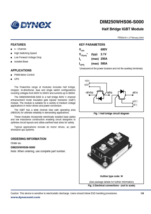
Caution: This device is sensitive to electrostatic discharge. Users should follow ESD handling procedures.1/8KEY PARAMETERS V CES 600V V CE(sat)*(typ)2.1VI C (max)250A I C(PK)(max)500A*(measured at the power busbars and not the auxiliary terminals)FEATURESI n - ChannelI High Switching Speed I Low Forward Voltage Drop IIsolated BaseAPPLICATIONSI PWM Motor Contro l IUPSThe Powerline range of modules includes half bridge,chopper, bi-directional, dual and single switch configurations covering voltages from 600V to 3300V and currents up to 3600A.The DIM250WHS06-S000 is a half bridge 600V n channel enhancement mode insulated gate bipolar transistor (IGBT)module. The module is suitable for a variety of medium voltage applications in motor drives and power conversion.The IGBT has a wide reverse bias safe operating area (RBSOA) for ultimate reliability in demanding applications.These modules incorporate electrically isolated base plates and low inductance construction enabling circuit designers to optimise circuit layouts and utilise earthed heat sinks for safety.Typical applications include dc motor drives, ac pwm drivesand ups systems.ORDERING INFORMATIONOrder as:DIM250WHS06-S000Note: When ordering, use complete part number.Fig. 1 Half bridge circuit diagramFig. 2 Electrical connections - (not to scale)Outline type code: W(See package details for further information)PDS5676-1.3 February 2004DIM250WHS06-S000Half Bridge IGBT ModuleDIM250WHS06-S0002/8Caution: This device is sensitive to electrostatic discharge. Users should follow ESD handling procedures.Test ConditionsV GE = 0V-T case = 65˚C 1ms, T case = 95˚C T case = 25˚C, T j = 150˚C V R = 0, t p = 10ms, T vj = 125˚CCommoned terminals to base plate. AC RMS, 1 min, 50Hz Symbol V CES V GES I C I C(PK)P max I 2t V isolABSOLUTE MAXIMUM RATINGS - PER ARMStresses above those listed under 'Absolute Maximum Ratings' may cause permanent damage to the device. In extreme conditions, as with all semiconductors, this may include potentially hazardous rupture of the package. Appropriate safety precautions should always be followed. Exposure to Absolute Maximum Ratings may affect device reliability.T case = 25˚C unless stated otherwise Units V V A A W kA 2s kVMax.600±202505001157TBD 2.5ParameterCollector-emitter voltage Gate-emitter voltage Continuous collector current Peak collector currentMax. transistor power dissipation Diode I 2t valueIsolation voltage - per moduleSymbol R th(j-c)R th(j-c)R th(c-h)T jT stg -Test ConditionsContinuous dissipation -junction to caseContinuous dissipation -junction to caseMounting torque 5Nm (with mounting grease)Transistor Diode-Mounting - M6Electrical connections - M6ParameterThermal resistance - transistorThermal resistance - diode Thermal resistance - case to heatsink (per module)Junction temperature Storage temperature range Screw torqueUnits ˚C/kW˚C/kW˚C/kW˚C ˚C ˚C Nm NmMax.1082031515012512555Typ.--------Min.-----–4032.5THERMAL AND MECHANICAL RATINGSInternal insulation: Al 2O 3Clearance: 13mmBaseplate material: Cu CTI (Critical Tracking Index): 175Creepage distance: 24mmDIM250WHS06-S000Caution: This device is sensitive to electrostatic discharge. Users should follow ESD handling procedures.3/8Note:†Measured at the power busbars and not the auxiliary terminals.L* is the circuit inductance + L MTest ConditionsV GE = 0V, V CE = V CESV GE = 0V, V CE = V CES , T case = 125˚CV GE = ±20V, V CE = 0V I C = 10mA, V GE = V CE V GE = 15V, I C = 250AV GE = 15V, I C = 250A, , T case = 125˚CDC t p = 1ms I F = 250AI F = 250A, T case = 125˚CV CE = 25V, V GE = 0V, f = 1MHz--ParameterCollector cut-off currentGate leakage current Gate threshold voltageCollector-emitter saturation voltageDiode forward currentDiode maximum forward current Diode forward voltageInput capacitance Module inductanceInternal transistor resistance - per armELECTRICAL CHARACTERISTICST case = 25˚C unless stated otherwise.Symbol I CESI GES V GE(TH)V CE(sat)†I F I FM V F †C ies L M R INTUnits mA mA µA V V V A A V V nF nH m ΩMax.11017.52.62.82505001.81.8--Typ.---5.52.12.3--1.51.527200.23Min.---4.5---------DIM250WHS06-S0004/8Caution: This device is sensitive to electrostatic discharge. Users should follow ESD handling procedures.Units ns ns mJ ns ns mJ µC µC A mJMax.----------Typ.60025020330130122151854Min.----------Test ConditionsI C = 250A V GE = ±15V V CE = 300V R G(ON) = R G(OFF) = 4.7ΩL ~ 100nHI F = 250A, V R = 300V,dI F /dt = 3600A/µs ParameterTurn-off delay time Fall timeTurn-off energy loss Turn-on delay time Rise timeTurn-on energy loss Gate chargeDiode reverse recovery charge Diode reverse currentDiode reverse recovery energyELECTRICAL CHARACTERISTICST case = 25˚C unless stated otherwise Symbol t d(off)t f E OFF t d(on)t r E ON Q g Q rr I rr E RECT case = 125˚C unless stated otherwise Units ns ns mJ ns ns mJ µC A mJMax.---------Typ.6505003040016018232005Min.---------Test ConditionsI C = 250A V GE = ±15V V CE = 300V R G(ON) = R G(OFF) = 4.7ΩL ~ 100nHI F = 250A, V R = 300V,dI F /dt = 3600A/µs ParameterTurn-off delay time Fall timeTurn-off energy loss Turn-on delay time Rise timeTurn-on energy lossDiode reverse recovery charge Diode reverse currentDiode reverse recovery energySymbol t d(off)t f E OFF t d(on)t r E ON Q rr I rr E RECDIM250WHS06-S000Caution: This device is sensitive to electrostatic discharge. Users should follow ESD handling procedures.5/8TYPICAL CHARACTERISTICSFig.3 Typical output characteristicsFig.4 Typical output characteristicsFig.4 Typical switching energy vs collector currentFig.5 Typical switching energy vs gate resistanceDIM250WHS06-S0006/8Caution: This device is sensitive to electrostatic discharge. Users should follow ESD handling procedures.Fig.6 Diode typical forward characteristicsDIM250WHS06-S000PACKAGE DETAILSFor further package information, please visit our website or contact Customer Services. All dimensions in mm, unless stated otherwise. DO NOT SCALE.Fig. 15 Package detailsCaution: This device is sensitive to electrostatic discharge. Users should follow ESD handling procedures.7/8POWER ASSEMBLY CAPABILITYThe Power Assembly group was set up to provide a support service for those customers requiring more than the basicsemiconductor, and has developed a flexible range of heatsink and clamping systems in line with advances in device voltages and current capability of our semiconductors.We offer an extensive range of air and liquid cooled assemblies covering the full range of circuit designs in general use today.The Assembly group offers high quality engineering support dedicated to designing new units to satisfy the growing needs of our customers.Using the latest CAD methods our team of design and applications engineers aim to provide the Power Assembly Complete Solution (PACs).HEATSINKSThe Power Assembly group has its own proprietary range of extruded aluminium heatsinks which have been designed to optimise the performance of Dynex semiconductors. Data with respect to air natural, forced air and liquid cooling (with flow rates) is available on request.For further information on device clamps, heatsinks and assemblies, please contact your nearest sales representative or Customer Services.CUSTOMER SERVICETel: +44 (0)1522 502753 / 502901. Fax: +44 (0)1522 500020SALES OFFICESBenelux, Italy & Switzerland: Tel: +33 (0)1 64 66 42 17. Fax: +33 (0)1 64 66 42 19.France: Tel: +33 (0)2 47 55 75 53. Fax: +33 (0)2 47 55 75 59.Germany, Northern Europe, Spain & Rest Of World: Tel: +44 (0)1522 502753 / 502901.Fax: +44 (0)1522 500020North America: Tel: (440) 259-2060. Fax: (440) 259-2059. Tel: (949) 733-3005. Fax: (949) 733-2986.These offices are supported by Representatives and Distributors in many countries world-wide.© Dynex Semiconductor 2003 TECHNICAL DOCUMENTATION – NOT FOR RESALE. PRODUCED IN UNITED KINGDOMHEADQUARTERS OPERATIONS DYNEX SEMICONDUCTOR LTD Doddington Road, Lincoln.Lincolnshire. LN6 3LF. United Kingdom.Tel: +44-(0)1522-500500Fax: +44-(0)1522-500550This publication is issued to provide information only which (unless agreed by the Company in writing) may not be used, applied or reproduced for any purpose nor form part of any order or contract nor to be regarded as a representation relating to the products or services concerned. No warranty or guarantee express or implied is made regarding the capability, performance or suitability of any product or service. The Company reserves the right to alter without prior notice the specification, design or price of any product or service. Information concerning possible methods of use is provided as a guide only and does not constitute any guarantee that such methods of use will be satisfactory in a specific piece of equipment. It is the user's responsibility to fully determine the performance and suitability of any equipment using such information and to ensure that any publication or data used is up to date and has not been superseded. These products are not suitable for use in any medical products whose failure to perform may result in significant injuryor death to the user. All products and materials are sold and services provided subject to the Company's conditions of sale, which are available on request.All brand names and product names used in this publication are trademarks, registered trademarks or trade names of their respective owners.e-mail:*****************************。


产品选型手册Product Selection Manual 2022.1101(Company Profile)公司发展历程0304深圳市美浦森半导体有限公司 2014年成立,总部位于深圳,是一家专业功率半导体元器件设计公司。
公司产品包括中大功率场效应管( 高中低压全系列产品, Trench MOSFET/SGT MOSFET /Super Junction MOSFET / Planar MOSFET),SiC 二极管、SiC MOSFET 等系列产品。
美浦森半导体在深圳/上海设有研发中心, 主要研发人员在产品研发和生产制程方面都具有丰富的行业经验, 平均行业经验在15年以上。
在深圳建立有半导体功率器件测试和应用实验室,主要负责产品的设计验证、参数测试、可靠性验证、系统分析、失效分析等,承担美浦森产品的研发质量验证。
目前,美浦森半导体MOSFET 和碳化硅系列产品在LED 电源、PD 电源、PC 和服务器电源、光伏逆变、UPS 、充电桩、智能家居、BLDC 、BMS 、小家电等领域得到广泛应用。
创新 高效 热爱 持续是美浦森半导体的核心价值; 用创新实现突破, 是公司不断前进的动力源泉。
专业于MOSFET 器件领域的拓展, 运用创新的电路设计和国际同步的研发技术, 成功研发出新一代MOSFET 系列产品, 产品相关性能达到行业领先水平。
我们始终坚持不断创新、不断突破, 始终保持产品第一、技术第一、服务第一的行业领先地位, 全心全意做好产品的开发与用户的极限体验 。
功率器件实验室&应用实验室投资2000万人民币兴建器件分析实验室和应用实验室, 负责美浦森产品的设计验证,品质监控和客户的技术支持。
2022年“美浦森实验室”将扩充至800平方, 并正在申请国家CNAS 认证实验室资格。
产品设计验证\产品性能比对\动静态参数测试\极限参数测试1可靠性验证\失效分析\产品品质监控2系统应用分析\系统性能验证3KEYENCE 显微镜KEYSIGHT 功率器件分析仪JUNO 直流参数测试系统ISPEC 高温反偏实验系统TEKTRONIX 功率器件动态测试仪STATEC 测试系统碳化硅全系6寸生产线升级结束, 碳化硅MOS 正式批量接单中低压Trench/SGT MOS 批量出货.超结MOS E7系列产品开始批量出货, RSP 参数超越竞品系列产品; 成立深圳器件测试及可靠性实验室、产品应用实验室.650V SiCDIODE 系列产品面市推广, 并大批量出货;1200V SiCDIODE 研发成功, 进入批量阶段; 碳化硅MOS 验证成功.2014年深圳市美浦森半导体有限公司成立,同年正式推广“美浦森”品牌MOS 系列产品.高压MOSFET (VDMOS )0605高压MOSFET (VDMOS )高压MOSFET 命名方式126245公司简称封装形式3额定电流P :TO -220F :TO -220F H:TO-247W:TO-3PD:D-Pak(TO-252)U:I-Pak(TO-251)B:D2-Pak(TO-263) I:I2-Pak(TO-262)沟道极性N:N-channel P:P-channel电压系数(x10)芯片工艺C:MOS C-FETU:MOS U-FET S:MOS S-FETUZ:MOS U-FET+ESD (Z: Zener diode)超结MOSFET (SJMOS )0708超结MOSFET 命名方式126245公司简称封装形式3额定电压P :TO -220 F :TO -220F H:TO-247W:TO-3P D:D-Pak(TO-252)U:I-Pak(TO-251)B:D2-Pak(TO-263)I :I2-Pak(TO-262)L :DFN8X8Rds (on )缩写Rds (on )数值单位:m 芯片工艺SJ:MOS SJ-FETE7:MOS E7-FET E7D:MOS FRDΩ超结产品特点Trr 时间缩短: 反向恢复时间快Qg 电荷小: 开关速度快,开关损耗小Rds (on )值小: 通态阻抗小,通态损耗小PKG体积小: 同等功率规格下封装小,有利于功率密度的提高超结MOSFET (SJMOS )27快恢复二极管(FRD)中低压MOSFET (MV/LV MOS )0910碳化硅二极管(SiC Diode)中低压命名方式126245公司简称封装形式3MOSFET电流值(1-3位数字)P:TO-220 F:TO-220FH:TO-247 W:TO-3PD:D-Pak(TO-252)U:I-Pak(TO-251)B:D2-Pak(TO-263)I :I2-Pak(TO-262)S:SOP-8 T:TSSOP-8M:DFN5X6 N:DFN3X3L:DFN8X8V:SOT-23沟通极性MOSFET电压值(2-3位数字)芯片工艺N:N-NchannelP:P-channelL:N-channel+P-channelD:Dual N-channelE:Dual P-channelT:普通Trench MOSFETG:Split Gate TrenchMOSFET27版本号只有一个版本时此为空,带ESD产品此位为K中低压MOSFET(MV/LV MOS)111213开关时间快,开关损耗小恢复时间短,Trr恢复时间短,趋近于零o工作结温高,工作温度可达到175C 以上击穿电压高,产品电压最高可达6000W 以上碳化硅MOSFET (SiC MOS )碳化硅MOSFET 命名方式5431212公司简称封装形式P :TO -220 F:TO -220F H:TO-247-3L W :TO -3P D:D-Pak(TO-252)U:I-Pak(TO-251)B:D2-Pak(TO-263)I : I2-Pak(TO-262)K: TO-247-4L453Rds(on)数值 单位: m 电压系数(X10)芯片工艺Ω碳化硅材料特点14碳化硅二极管命名方式1245公司简称封装形式3额定电流P :TO -220 F :TO -220FH:TO-247 L :DFN8X8D:D-Pak(TO-252)U:I-Pak(TO-251)B:D2-Pak(TO-263)M:DFN5x67S: SO-7N: 内绝缘工艺电压系数(X10)芯片工艺V1:JBS G1: MPS1:2Pin2P :TO -2202F :TO -220F 2H:TO-2472B:D2-Pak 2I:I2-Pak2:3Pin 2Chip2TP :TO -2202TW :TO -3P 2TH: TO-2473:2Pin 2ChipR :TO -220RF :TO-220F RH :TO -2474:3Pin 1Chip。

Surface MountSchottky Power RectifierSMA Power Surface Mount PackageMBRA340, NRVBA340,NRVBA340NEmploying the Schottky Barrier principle in a large area metal −to −silicon power diode. State of the art geometry features epitaxial construction with oxide passivation and metal overlay contact. Ideally suited for low voltage, high frequency rectification, or as free wheeling and polarity diodes in surface mount applications where compact size and weight are critical to the system.Features•Small Compact Surface Mountable Package with J −Bent Leads •Rectangular Package for Automated Handling •Highly Stable Oxide Passivated Junction •Very Low Forward V oltage Drop •Guardring for Stress Protection•NRVBA Prefix for Automotive and Other Applications Requiring Unique Site and Control Change Requirements; AEC −Q101Qualified and PPAP Capable*•These Devices are Pb −Free, Halogen Free/BFR Free and are RoHS CompliantMechanical Characteristics:•Case: Epoxy, Molded•Weight: 70 mg (approximately)•Finish: All External Surfaces Corrosion Resistant and Terminal Leads are Readily Solderable•Lead and Mounting Surface Temperature for Soldering Purposes:260°C Max. for 10 Seconds•Polarity: Cathode Lead Indicated by Polarity Band •ESD Ratings:♦Machine Model = C♦Human Body Model = 3B•Device Meets MSL 1 RequirementsDevicePackageShipping †ORDERING INFORMATIONSCHOTTKY BARRIERRECTIFIER 3.0 AMPERES 40 VOLTSMARKING DIAGRAMSMA CASE 403D STYLE 1A34AYWWGMBRA340T3G NRVBA340T3G NRVBA340T3G −VF01NRVBA340NT3G*Cathode AnodeA34= Device Code A = Assembly Location**Y = Year WW = Work Week G = Pb −Free Package12SMA (Pb −Free)5,000 / Tape & Reel†For information on tape and reel specifications,including part orientation and tape sizes, please refer to our Tape and Reel Packaging Specification Brochure, BRD8011/D.**The Assembly Location code (A) is front side optional. In cases where the Assembly Location is stamped in the package bottom (molding ejecter pin),the front side assembly code may be blank.(Note: Microdot may be in either location)MAXIMUM RATINGSRatingSymbol Value Unit Peak Repetitive Reverse Voltage Working Peak Reverse Voltage DC Blocking VoltageV RRM V RWM V R 40VAverage Rectified Forward Current (At Rated V R , T L = 100°C)I O 3.0A Non −Repetitive Peak Surge Current(Surge Applied at Rated Load Conditions Halfwave, Single Phase, 60 Hz)I FSM 100A Storage/Operating Case Temperature T stg , T C −55 to +150°C Operating Junction Temperature (Note 1)T J −55 to +150°C Voltage Rate of Change (Rated V R , T J = 25°C)dv/dt10,000V/m sStresses exceeding those listed in the Maximum Ratings table may damage the device. If any of these limits are exceeded, device functionality should not be assumed, damage may occur and reliability may be affected.1.The heat generated must be less than the thermal conductivity from Junction −to −Ambient: dP D /dT J < 1/R q JA .THERMAL CHARACTERISTICSCharacteristicSymbol Value Unit Thermal Resistance − Junction −to −Lead (Note 2)Thermal Resistance − Junction −to −Ambient (Note 2)R θJL R θJA1581°C/W2.Mounted on 2″ Square PC Board with 1″ Square Total Pad Size, PC Board FR4.ELECTRICAL CHARACTERISTICSCharacteristicSymbol ValueUnit Maximum Instantaneous Forward Voltage (Note 3)(I F = 3.0 A)V FT J = 25°C T J = 100°C Volts0.4500.390Maximum Instantaneous Reverse Current (V R = 40 V)I R T J = 25°CT J = 100°CmA 0.315Product parametric performance is indicated in the Electrical Characteristics for the listed test conditions, unless otherwise noted. Product performance may not be indicated by the Electrical Characteristics if operated under different conditions.3.Pulse Test: Pulse Width ≤ 250 μs, Duty Cycle ≤ 2.0%.TYPICAL CHARACTERISTICSFigure 1. Typical Forward VoltageFigure 2. Maximum Forward Voltage1010.1V F , INSTANTANEOUS FORWARD VOLTAGE (VOLTS)I F , IN S T A N T A N E O U S F O R W A R D C U R R E N T (A M P S )1010.1V F , MAXIMUM INSTANTANEOUS FORWARDVOLTAGE (VOLTS)I F , I N S T A N T A N E O U S F O R W A R D C U R R E N T (A M P S )Figure 3. Typical Reverse CurrentFigure 4. Maximum Reverse CurrentV R , REVERSE VOLTAGE (VOLTS)100E −10E −10E −100E −I R , R E V E R S E C U R R E N T (A M P S )100E −100E −1E −1E −10E −1E −V R , REVERSE VOLTAGE (VOLTS)100E −10E −10E −100E −I R )1E −1E −Figure 5. Current Derating02.5I O , A V E R A G E F O R W A R D C U R R E N T (A M P S )T L , LEAD TEMPERATURE (°C)Figure 6. Forward Power Dissipation1.800.6I O , AVERAGE FORWARD CURRENT (AMPS)P F O , A V E R A G E P O W E R D I S S I P A T I O N (W A T T S )Figure 7. Capacitance0.511.52533.54.50.20.41.00.81.6Figure 8. Typical Operating TemperatureDeratingV R , REVERSE VOLTAGE (VOLTS)C , C A P A C I T A N C E (p F )V R , DC REVERSE VOLTAGE (VOLTS)115T J , D E R A T E D O P E R A T I N G T E M P E R A T U R E (°C )1.41.24Figure 9. Thermal Response, Junction −to −Ambient (min pad)t, TIME (S)R (t ), T R A N S I E N T T H E R M A L R E S I S T A N C E (°C /W )Figure 10. Thermal Response, Junction to Ambient (1 inch pad)t, TIME (S)R (t ), T R A N S I E N T T H E R M A L R E S I S T A N C E (°C /W )1100SCALE 1:1SMA CASE 403D ISSUE JDATE 22 OCT 2021xxxx = Specific Device Code A = Assembly Location Y = YearWW = Work WeekG= Pb −Free PackageSTYLE 1:PIN 1.CATHODE (POLARITY BAND)2.ANODESTYLE 2:NO POLARITYSTYLE 1STYLE 2STYLE 1STYLE 2xxxx AYWWG xxxx AYWW G GENERICMARKING DIAGRAM**This information is generic. Please refer to device data sheet for actual part marking.Pb −Free indicator, “G” or microdot “G ”, may or may not be present. Some products maynot follow the Generic Marking.MECHANICAL CASE OUTLINEPACKAGE DIMENSIONSPUBLICATION ORDERING INFORMATIONTECHNICAL SUPPORTNorth American Technical Support:Voice Mail: 1 800−282−9855 Toll Free USA/Canada Phone: 011 421 33 790 2910LITERATURE FULFILLMENT :Email Requests to:*******************onsemi Website: Europe, Middle East and Africa Technical Support:Phone: 00421 33 790 2910For additional information, please contact your local Sales Representative。

全球LED驱动IC规格书下载大全编辑文子目录台湾地区部分: 4点晶科技股份有限公司 4台湾聚积科技公司 4台湾广鹏(富晶)科技公司 5台湾台晶科技 5台湾易亨电子公司 5台湾圆创科技股份有限公司 5台湾晶锜科技公司 6天鈺科技股份有限公司 6台湾飞虹积体电路有限公司 6台湾芯瑞科技股份有限公司 6台湾茂达电子公司 6日本部分: 6东芝公司 6松下电器产业株式会社半导体社 6美国部分: 7IR 国际整流器公司 7ON 安森美半导体 7美国超科公司 (SUPERTEX 7TI 美国德州仪器公司屏幕驱动部分 8 TI 美国德州仪器公司白光LED驱动器 8美国美信集成产品公司白光LED驱动器 9美国美信集成产品公司高亮度LED驱动器 9美国国家半导体公司新产品: 10美国国家半导体公司白色LED低功率驱动部分 10美国国家半导体公司照明管理单元(LMU) 11美国凌特公司白光背光及背光指示部分: 12美国凌特公司全彩背光部分: 12美国凌特公司大电流驱动及LED闪光灯部分: 13飞兆半导体公司 13ADI 美国模拟器件公司 14美国 SIPEX 公司 14美国PI ( POWER INTEGRATIONS公司 14美国PI ( POWER INTEGRATIONS公司数据手册 14美国PI ( POWER INTEGRATIONS公司IC 产品系列参考 14美国加州ZYWYN 公司 (美商齐荣小屏背光部分 15美国加州ZYWYN 公司(美商齐荣大尺寸嵌入式背光部分 15美国加州ZYWYN 公司(美商齐荣工业照明部分 15美国灿瑞科技公司 15美商茂力公司(MPS 16美国CATALYST 16欧洲英国IXYS半导体公司 17美国迈瑞半导体公司 17欧洲部分: 17德国英飞凌 17奥地利微电子 17NXP 荷兰皇家飞利浦公司I²C LED 显示控制 17NXP 荷兰皇家飞利浦公司高功率系统用 SMPS 芯片 17ST 意法半导体公司显示器驱动器 18英国ZETEX(捷特科)公司 18国内部分: 18杭州士兰微电子有限公司 18深圳泉芯电子技木有限公司 18深圳光华源科技有限公司 18深圳国微电子股份有限公司 19深圳市彩拓科技开发有限公司 19华润矽威科技(上海)有限公司 19深圳市安联创科技有限公司 19LED屏幕配套部分逻辑IC,飞利浦些列: 19LED 驱动配套部分 MOS管: 19台湾地区部分:点晶科技股份有限公司DD311 单信道大功率恒流驱动IC最大1A最高耐压36V线性恒流IC 规格书DD312 单信道大功率恒流驱动IC最大1A最高耐压18V线性恒流IC 规格书DD313 三信道大功率恒流驱动IC 500mA R/G/B恒流驱动IC 规格书DM412 三通道装饰照明专用可直接数据级联恒流IC 200mA R/G/B恒流驱动IC 规格书DM413 三通道装饰照明专用PWM输出驱动IC 100mA R/G/B恒流驱动IC 规格书DM114A,DM115A 新版8位驱动IC 主要是用于屏幕及灯饰规格书DM115B通用8位恒流驱动IC 恒流一致性及稳定性高规格书DM11C 8位驱动IC 具有短断点侦测及温度保护功能,屏幕灯饰使用规格书DM13C 16位驱动IC 具有短断点侦测及温度保护功能,屏幕灯饰使用规格书DM13A 16位恒流驱动,面对低端屏幕客户规格书DM134,DM135, DM136 16位驱动IC 主要用于LED屏幕及护栏管规格书DM132 16位1024级PWM输出驱动IC 规格书DM137 16位开,短路,过温智能侦测驱动IC 规格书DM133 16位开路检测&64级电流调整&过温警示驱动IC 规格书DM163 8x3信道4096级PWM驱动IC 规格书DM621 4×3装饰照明专用PWM输出驱动恒流IC 规格书DM631 12比特内置PWM+实时检测恒流驱动IC 规格书DM632 16比特内置PWM+实时检测恒流驱动IC 规格书DM163 8×3通道4096级PWM输出恒流驱动IC 规格书DM164 8×3通道4096级PWM输出恒流驱动IC 规格书DD211 二倍升压驱动IC 2-3.3V 最大升压100mA固定式恒流IC 规格书DD231 3信道驱动IC 5-30mA 可设置小体上电即亮型IC 规格书DD233 4信道驱动IC 5-30mA 可设置小体、可开关型IC 规格书DD212 1.5-5.5V二倍升压最大400mA电流输出驱动单颗LED恒流IC 规格书PC112,PC113 2.8-5V四倍升压驱动20mA小功率多颗LED恒流IC 规格书ST2225A 35输出信道之数字/字母LED驱动芯片规格书台湾聚积科技公司MBI1801 1路恒流驱动1.2A电流可设定PWM信号灰度调节规格书MBI1802 2路恒流驱动360mA电流可两路单独设定PWM信号灰度调节规格书MBI1804 4路恒流驱动240mA电流可设定PWM信号灰度调节规格书MBI1816 16路恒流驱动电流可设定PWM信号灰度调节规格书MBI5016 16位最大90mA LED屏幕、护栏灯管恒流驱动IC 已停产规格书MBI5024 面对低端客户16位LED屏幕、护栏灯管恒流驱动IC 规格书MBI5025 16位最大45mALED屏幕、护栏灯管恒流驱动IC 规格书MBI5026 16位最大90mA LED屏幕、护栏灯管恒流驱动IC 规格书MBI5028 16位最大90mA LED屏幕、护栏灯管恒流驱动IC,具电流增益功能规格书MBI5030 16位内置PWM高灰阶LED恒流驱动IC 规格书MBI5031 16位内置PWM高灰阶LED恒流驱动IC,相对5030低端客户规格书MBI5039MBI5168 8位LED屏幕、护栏灯管恒流驱动IC 规格书MBI6010 3位级联式LED灯饰屏幕,R/G/B单独电流可设置恒流驱动IC 规格书台湾广鹏(富晶)科技公司A701、A702 固定式5-30mA灯饰恒流规格书A703 120mA可开式6-50V降压型恒流IC 规格书A705 220mA、2.7-12V固定降压型单路恒流IC 规格书A706 5-40mA、5-50V/PWM多路可开关型恒流IC 规格书AMC711x 固定式小电流灯饰应用规格书AMC711x_E固定式小电流灯饰应用规格书AMC7135 2-6V 低压差固定式恒流驱动IC 1颗LED 规格书AMC7140 5-50V DC&DC 最大500mA电流可调,1颗或多颗LED驱动IC 规格书AMC7150 5-24V DC&DC 最大1.5A固定式, 1-3颗LED驱动IC 规格书AMC7169 LED保护IC 规格书台湾台晶科技T6309A 手机背光规格书T6309B 手机背光规格书T6313A 手机背光规格书T6319A 手机背光 LED并联固定电压背光驱动IC 规格书T6311A 路灯规格书T6316A/B 路灯规格书T6326A 手电式设备低压差电流多路可调400mA 规格书T6335A 矿灯低压差恒流式与AMC7135相同规格书T6336A 草坪灯用于主付灯矿灯规格书T6315A 草坪灯规格书T6317A MR16-1W 7-24V 350mA 1W多颗驱动IC 规格书T6325A MR16-3/5W 7-24V 700mA 多颗LED驱动IC 规格书T6327A 矿灯主付灯多电流可选固定式低压差是LED恒流驱动规格书T6329A磷酸铁锂电池矿灯升压式LED驱动恒流IC 规格书台湾易亨电子公司台湾圆创科技股份有限公司AT1325 8-bit Constant Current LED Sink Driver 规格书AT1326 16-bit Constant Current LED Sink Driver 规格书AT1313 Constant current LED driver 规格书AT1312 Boost constant current LED driver 规格书AT1314 Buck constant current LED driver 规格书台湾晶锜科技公司SCT2024 16位移位LED恒流驱动,适合目前LED大屏幕使用3-40mA 规格书SCT2026 16位移位LED恒流驱动,适合目前LED大屏幕使用3-90mA规格书SCT2210 16位移位LED恒流驱动,适合LED大屏幕及插件护栏管使用3-120mA 规格书SCT2110 8位移位LED恒流驱动IC,主要用于灯饰产品规格书SCT2512 12位移位护栏管专用IC,3路OE灰度可以单独调节规格书SCT2007 3路点光源驱动IC,可兼容MIB6010 规格书天鈺科技股份有限公司FP6742A 输入4.5-25V,输出8路小功率背光源升压驱动IC 规格书FP6742 输入4.5-25V,输出6路小功率背光源升压驱动IC 规格书FP6741 输入4.5-25V,输出10路小功率背光源升压驱动IC 规格书FP6732FP6700 高压驱动IC(类似HV9910)规格书FP6735 输入2.8-5.5升压驱动10pcs 25mA 规格书台湾飞虹积体电路有限公司台湾芯瑞科技股份有限公司SMD733 3-40V电压输入,内置MOS管降压型驱动电流1A 规格书SMD735 3-40V电压输入,降压型驱动电流700mA(可替代AMC7150)规格书SMD736 最高40V电压输入,内置MOS管降压型驱动电流3A 规格书SMD802 市电直驱1A LED驱动IC(可替代HV9910)规格书SMD911 市电直驱IC,外置MOS LED隔离方案驱动IC 规格书SMD912 市电隔离型直驱IC,外置MOS LED驱动IC 规格书台湾茂达电子公司APW7003APW7008APW7071APW7005日本部分:东芝公司TB62725 8位移位恒流驱动IC 规格书TB62726AN/AF 16位全彩LED大屏幕规格书TB62726ANG/AFG 16位全彩LED大屏幕规格书TCA62746AFG/AFNG 16位全彩LED大屏幕带断、短路侦测及温度保护规格书松下电器产业株式会社半导体社MIP551 电压输入(80~280 VAC)输出电流0.5 A 多颗LED应用规格书MIP552 电压输入(80~280 VAC)输出电流1 A 多颗LED应用规格书美国部分:IR 国际整流器公司IRS2540 200V市电直驱1W多颗LED驱动IC,500mA 规格书IRS2541 600V市电直驱1W多颗LED驱动IC,500mA 规格书ON 安森美半导体NCP5612 2通道泵式可PWM的白色LED驱动产品是LCD屏背光照明,操作模态 1 x 和 1.5 x 泵式驱动,87% 效率连同 0.2% 相配误差。


MMBZ5221BLT1 SeriesPreferred DeviceZener Voltage Regulators 225 mW SOT−23 Surface MountThis series of Zener diodes is offered in the convenient, surface mount plastic SOT−23 package. These devices are designed to provide voltage regulation with minimum space requirement. They are well suited for applications such as cellular phones, hand held portables, and high density PC boards.Features•225 mW Rating on FR−4 or FR−5 Board•Zener V oltage Range − 2.4 V to 91 V•Package Designed for Optimal Automated Board Assembly •Small Package Size for High Density Applications•ESD Rating of Class 3 (>16 KV) per Human Body Model •Pb−Free Packages are AvailableMechanical CharacteristicsCASE:V oid-free, transfer-molded, thermosetting plastic case FINISH:Corrosion resistant finish, easily solderableMAXIMUM CASE TEMPERATURE FOR SOLDERING PURPOSES: 260°C for 10 SecondsPOLARITY:Cathode indicated by polarity bandFLAMMABILITY RATING:UL 94 V−0MAXIMUM RATINGSRating Symbol Max UnitTotal Power Dissipation on FR−5 Board, (Note 1) @ T A = 25°CDerated above 25°C P D2251.8mWmW/°CThermal Resistance,Junction−to−AmbientR q JA556°C/WTotal Power Dissipation on Alumina Substrate, (Note 2) @ T A = 25°C Derated above 25°C P D3002.4mWmW/°CThermal Resistance, Junction−to−Ambient Rq JA417°C/WJunction and StorageTemperature RangeT J, T stg−65 to +150°CMaximum ratings are those values beyond which device damage can occur.Maximum ratings applied to the device are individual stress limit values (notnormal operating conditions) and are not valid simultaneously. If these limitsare exceeded, device functional operation is not implied, damage may occurand reliability may be affected.1.FR−5 = 1.0 X 0.75 X 0.62 in.2.Alumina = 0.4 X 0.3 X 0.024 in, 99.5% alumina.Devices listed in bold, italic are ON SemiconductorPreferred devices. Preferred devices are recommendedchoices for future use and best overall value.ELECTRICAL CHARACTERISTICS(Pinout: 1-Anode, 2-No Connection, 3-Cathode)(T A = 25°C unless otherwise noted, V F = 0.95 V Max. @ I F = 10 mA) Symbol ParameterV Z Reverse Zener Voltage @ I ZTI ZTReverse CurrentZ ZT Maximum Zener Impedance @ I ZT I ZK Reverse CurrentZ ZK Maximum Zener Impedance @ I ZK I R Reverse Leakage Current @ V R V R Reverse VoltageI F Forward CurrentV F Forward Voltage @ I FELECTRICAL CHARACTERISTICS (Pinout: 1-Anode, 2-NC, 3-Cathode)(V F = 0.9 V Max @ I F = 10 mA for all types.)DeviceDeviceMarkingZener Voltage (Note 3)Zener Impedance Leakage CurrentV Z (Volts)@ I ZT Z ZT @ I ZT Z ZK @ I ZK I R @ V R Min Nom Max mA W W mA m A VoltsMMBZ5221BL, G18A 2.28 2.4 2.52203012000.251001 MMBZ5222BL, G18B 2.37 2.5 2.63203012500.251001 MMBZ5223BL, G18C 2.56 2.7 2.84203013000.25751 MMBZ5224BL, G18D 2.66 2.8 2.94203014000.25751 MMBZ5225BL, G18E 2.853 3.152********.25501 MMBZ5226BL, G8A 3.13 3.3 3.47202816000.25251 MMBZ5227BL, G8B 3.42 3.6 3.78202417000.25151 MMBZ5228BL, G8C 3.70 3.9 4.10202319000.25101 MMBZ5229BL, G8D 4.08 4.3 4.52202220000.2551 MMBZ5230BL, G8E 4.46 4.7 4.94201919000.2552 MMBZ5231BL, G8F 4.84 5.1 5.36201716000.2552 MMBZ5232BL, G8G 5.32 5.6 5.88201116000.2553 MMBZ5233BL, G8H 5.706 6.3020716000.255 3.5 MMBZ5234BL, G8J 5.89 6.2 6.5120710000.2554 MMBZ5235BL, G8K 6.46 6.87.142057500.2535 MMBZ5236BL, G8L7.127.57.882065000.2536 MMBZ5237BL, G8M7.798.28.612085000.253 6.5 MMBZ5238BL, G8N8.268.79.142086000.253 6.5 MMBZ5239BL, G8P8.649.19.5620106000.2537 MMBZ5240BL, G8Q9.501010.5020176000.2538 MMBZ5241BL, G8R10.41111.5520226000.2528.4 MMBZ5242BL, G8S11.401212.6020306000.2519.1 MMBZ5243BL, G8T12.351313.659.5136000.250.59.9 MMBZ5244BL, G8U13.301414.709156000.250.110 MMBZ5245BL, G8V14.251515.758.5166000.250.111 MMBZ5246BL, G8W15.201616.807.8176000.250.112 MMBZ5247BL, G8X16.151717.857.4196000.250.113 MMBZ5248BL,G8Y17.101818.907216000.250.114 MMBZ5249BL, G8Z18.051919.95 6.6236000.250.114 MMBZ5250BL,G81A19.002021.00 6.2256000.250.115 MMBZ5251BL, G81B20.902223.10 5.6296000.250.117 MMBZ5252BL, G81C22.802425.20 5.2336000.250.118 MMBZ5253BL, G81D23.752526.255356000.250.119 MMBZ5254BL, G81E25.652728.35 4.6416000.250.121 MMBZ5255BL, G81F26.602829.40 4.5446000.250.121 MMBZ5256BL, G81G28.503031.50 4.2496000.250.123 MMBZ5257BL, G81H31.353334.65 3.8587000.250.125 MMBZ5258BL, G81J34.203637.80 3.4707000.250.127 MMBZ5259BL, G81K37.053940.95 3.2808000.250.130 MMBZ5260BL, G81L40.854345.153939000.250.133 MMBZ5261BL, G81M44.654749.35 2.710510000.250.136 MMBZ5262BL, G81N48.455153.55 2.512511000.250.139 MMBZ5263BL, G81P53.205658.80 2.215013000.250.143 MMBZ5264BL, G81Q57.006063.00 2.117014000.250.146 MMBZ5265BL, G81R58.906265.10218514000.250.147 MMBZ5266BL, G81S64.606871.40 1.823016000.250.152 MMBZ5267BL, G81T71.257578.75 1.727017000.250.156 MMBZ5268BL, G81U77.908286.10 1.533020000.250.162 MMBZ5270BL, G81W86.459195.55 1.440023000.250.169 3.Zener voltage is measured with a pulse test current I Z at an ambient temperature of 25°CNOTE:MMBZ5233BLT1, MMBZ5246BLT1, MMBZ5251BLT1, and MMBZ5252BLT1 Not Available in 10,000/Tape & Reel.†The “G” suffix indicates Pb−Free package available.V Z , T E M P E R A T U R E C O E F F I C I E N T (m V /C )°θV Z , NOMINAL ZENER VOLTAGE (V)− 3− 2−1012345678Figure 1. Temperature Coefficients (Temperature Range −55°C to +150°C)V Z , T E M P E R A T U R E C O E F F I C I E N T (m V /C)°θ100101V Z , NOMINAL ZENER VOLTAGE (V)Figure 2. Temperature Coefficients (Temperature Range −55°C to +150°C)V Z , NOMINAL ZENER VOLTAGEFigure 3. Effect of Zener Voltage onZener ImpedanceZ Z T , D Y N A M I C I M P E D A N C E ()Ω1000100101V F , FORWARD VOLTAGE (V)Figure 4. Typical Forward VoltageC , C A P A C I T A N C E (p F )1000100101V Z , ZENER VOLTAGE (V)I Z , Z E N E R C U R R E N T (m A )V Z , ZENER VOLTAGE (V)1001010.10.01I R , L E A K A G E C U R R E N T (A )μV Z , NOMINAL ZENER VOLTAGE (V)Figure 6. Typical Leakage Current10001001010.10.010.0010.00010.00001I Z , Z E N E R C U R R E N T (m A )Figure 7. Zener Voltage versus Zener Current(V Z Up to 12 V)Figure 8. Zener Voltage versus Zener Current(12 V to 91 V)PACKAGE DIMENSIONSSOT−23 (TO−236)CASE 318−08ISSUE AL*For additional information on our Pb−Free strategy and solderingdetails, please download the ON Semiconductor Soldering and Mounting Techniques Reference Manual, SOLDERRM/D.SOLDERING FOOTPRINT*ǒmm inchesǓSCALE 10:1bNOTES:1.DIMENSIONING AND TOLERANCING PER ANSI ON Semiconductor and are registered trademarks of Semiconductor Components Industries, LLC (SCILLC). SCILLC reserves the right to make changes without further notice to any products herein. SCILLC makes no warranty, representation or guarantee regarding the suitability of its products for any particular purpose, nor does SCILLC assume any liability arising out of the application or use of any product or circuit, and specifically disclaims any and all liability, including without limitation special, consequential or incidental damages.“Typical” parameters which may be provided in SCILLC data sheets and/or specifications can and do vary in different applications and actual performance may vary over time. All operating parameters, including “Typicals” must be validated for each customer application by customer’s technical experts. SCILLC does not convey any license under its patent rights nor the rights of others. SCILLC products are not designed, intended, or authorized for use as components in systems intended for surgical implant into the body, or other applications intended to support or sustain life, or for any other application in which the failure of the SCILLC product could create a situation where personal injury or death may occur. Should Buyer purchase or use SCILLC products for any such unintended or unauthorized application, Buyer shall indemnify and hold SCILLC and its officers, employees, subsidiaries, affiliates,and distributors harmless against all claims, costs, damages, and expenses, and reasonable attorney fees arising out of, directly or indirectly, any claim of personal injury or death associated with such unintended or unauthorized use, even if such claim alleges that SCILLC was negligent regarding the design or manufacture of the part. SCILLC is an Equal Opportunity/Affirmative Action Employer. This literature is subject to all applicable copyright laws and is not for resale in any manner.PUBLICATION ORDERING INFORMATION。

XPT TM 600V IGBT GenX3TMCES I C110= 100A V CE(sat) ≤ 1.80V t fi(typ)= 150nsSymbol Test ConditionsMaximum Ratings V CES T J = 25°C to 175°C600V V CGR T J = 25°C to 175°C, R GE = 1M Ω 600V V GES Continuous ±20V V GEM Transient±30VI C25T C = 25°C (Chip Capability) 220 A I LRMS Terminal Current Limit 160 A I C110T C = 110°C 100A I CM T C = 25°C, 1ms 480A I A T C = 25°C 50 A E AST C = 25°C 600 mJSSOA V GE = 15V, T VJ = 150°C, R G = 2Ω I CM = 200A(RBSOA) Clamped Inductive Load @ ≤ V CES t scV GE = 15V, V CE = 360V, T J = 150°C 10 μs (SCSOA)R G = 10Ω, Non Repetitive P C T C = 25°C830W T J -55 ... +175°C T JM 175°C T stg -55 ... +175°CT LMaximum Lead Temperature for Soldering 300°CT SOLD 1.6 mm (0.062in.) from Case for 10s 260 °C M d Mounting Torque1.13/10Nm/lb.in.Weight6gExtreme Light Punch Through IGBT for 10-30 kHz SwitchingSymbol Test Conditions Characteristic Values (T J = 25°C, Unless Otherwise Specified) Min. Typ. Max.BV CES I C = 250μA, V GE = 0V 600 VV GE(th)I C= 250μA, V CE = V GE3.05.5VI CES V CE = V CES , V GE = 0V25μAT J = 150°C 2 mA I GESV CE = 0V, V GE = ±20V±100 nAV CE(sat)I C = 70A, V GE = 15V, Note 11.50 1.80 V T J = 150°C1.77 VFeaturesz Optimized for 10-30kHz Switching z Square RBSOA z Avalanche Ratedz Short Circuit Capabilityz High Current Handling Capability zInternational Standard PackageAdvantagesz High Power DensityzLow Gate Drive RequirementApplicationsz Power Inverters z UPSz Motor Drives z SMPSzPFC Circuits z Battery Chargers z Welding Machines zLamp BallastsG = Gate C = Collector E = Emitter Tab = CollectorTO-247 ADIXYS Reserves the Right to Change Limits, Test Conditions, and Dimensions.Symbol Test Conditions (T J = 25°C Unless Otherwise Specified)fs I C = 60A , V CE C ie sC oes V CE = 25V, V GE C resQ g(on)Q ge I C = 70A , V GE Q gc d(on)Notes:1. Pulse test, t ≤ 300μs, duty cycle, d ≤ 2%.2. Switching times & energy losses may increase for higher V CE (clamp), T J or R G .Fig. 1. Output Characteristics @ T 6080100120140I C - A m p e r e sFig. 7. Transconductance304050607080g f s - S i e m e n sFig. 13. Inductive Switching Energy Loss vs.Gate Resistance2.53.03.54.04.5E o f f - M i l l i J o u l e sE off E on - - - - T J = 150ºC , V GE = 15V V CE = 360VIIXYS Reserves the Right to Change Limits, Test Conditions, and Dimensions.Fig. 19. Inductive Turn-on Switching Times vs.Gate Resistance80100120140160180r i - N a n o s e c o n d st r i t d(on) - - - -T J = 150ºC, V GE = 15V V CE = 360V。

SVD501DEAG 说明书30mA 、600V N 沟道耗尽型场效应管描述SVD501DEAG N 沟道耗尽型高压功率MOS 场效应晶体管,采用士兰微电子的平面高压VDMOS 工艺技术制造。
先进的工艺及原胞结构使得该产品具有较低的导通电阻、优越的开关性能及很高的雪崩击穿耐量。
该产品可广泛应用于电子镇流器,低功率开关电源。
特点♦ 30mA ,600V ♦ 耗尽型(常开器件) ♦ 提升了ESD 能力 ♦开关速度快♦提升了dv/dt 能力命名规则产品规格分类产品名称 封装形式 打印名称 环保等级 包装 SVD501DEAGTRSOT-23501DE无卤编带极限参数参数名称符号参数范围单位漏源电压V DS600 V 栅源电压V GS±20 V漏极电流T C=25°CI D0.03A T C=70°C 0.024漏极冲击电流I DM0.12 A耗散功率(T C=25°C)-大于25°C每摄氏度减少P D0.8 W0.007 W/°C工作结温范围T J-55~+150 °C 贮存温度范围T stg-55~+150 °C热阻特性参数名称符号参数范围单位芯片对管壳热阻RθJC150 °C/W 芯片对环境的热阻RθJA250 °C/W 电性参数(除非特殊说明,TC=25°C)参数名称符号测试条件最小值典型值最大值单位漏源击穿电压BV DSS V GS=-5V,I D=250µA 600 -- -- V 漏源漏电流I D(off)V DS=600V,V GS=-5V -- -- 0.1 µA 栅源漏电流I GSS V GS=±20V,V DS=0V -- -- ±10 µA 栅极阈值电压V GS(th)V DS=3V,I D=8µA -2.7 -- -1.0 V 导通漏极电流I DSS V GS=0V,V DS=25V 12 -- -- mA导通电阻R DS(on)V GS=0V,I D=3mA -- 310 700ΩV GS=10V,I D=16mA -- 330 700输入电容C issV DS=25V,V GS=-5V,f=1.0MHZ -- 10.03pF输出电容C oss-- 2.92 反向传输电容C rss-- 0.12开启延迟时间t d(on)V DD=300V,I D=0.01AV GS=-5~7VR G=6Ω(注1,2) -- 12.36ns开启上升时间t r-- 60.44 关断延迟时间t d(off)-- 25.48 关断下降时间t f-- 100栅极电荷量Q g V DS=400V,I D=0.01AV GS=-5~7V(注1,2) -- 2.75nC栅极-源极电荷量Q gs-- 0.55 栅极-漏极电荷量Q gd-- 1.61源-漏二极管特性参数参数名称符号测试条件最小值典型值最大值单位源极电流I S MOS管中源极、漏极构成的反偏P-N结-- -- 0.03A源极脉冲电流I SM-- -- 0.12源-漏二极管压降V SD I F=16mA,V GS=-5V -- -- 1.2 V反向恢复时间T rr I F=0.01A,V R=300V,dI F/dt=100A/µs -- -- 367 ns反向恢复电荷Q rr-- -- 963 nC 注:1. 脉冲测试:脉冲宽度≤300μs,占空比≤2%;2. 基本不受工作温度的影响。


Parameter Absolute Maximum Ratings T A =25°C unless otherwise noted Drain-Source Voltage DGDS AOT12N40Peak diode recovery dv/dtGate-Source Voltage T C =100°CPulsed Drain Current C Continuous Drain CurrentT C =25°C Avalanche CurrentCSingle pulsed avalanche energy G Repetitive avalanche energyCSymbolMinTypMaxUnits400500BV DSS /∆TJ 0.4V/ o C 110I GSS Gate-Body leakage current ±100n ΑV GS(th)Gate Threshold Voltage3.33.94.5V R DS(ON)0.490.59Ωg FS 10S V SD 0.721V I S Maximum Body-Diode Continuous Current11A I SM28A C iss 7409251110pF C oss 70100130pF C rss 3.5 6.49.0pF R g1.42.9 4.5ΩQ g 131721nC Q gs 5.4nC Q gd 5.7nC t D(on)25ns t r 57ns t 41ns V DS =40V, I D =6A Forward Transconductance Electrical Characteristics (T J =25°C unless otherwise noted)STATIC PARAMETERS ParameterConditionsV DS =5V, I D =250µA V DS =320V, T J =125°C Zero Gate Voltage Drain Current I DSS Zero Gate Voltage Drain Current V DS =400V, V GS =0V ID=250µA, VGS=0V BV DSS Static Drain-Source On-Resistance V GS =10V, I D =6A Diode Forward VoltageTurn-Off DelayTime V GS =10V, V DS =200V, I D =12A,R G =25ΩGate resistanceV GS =0V, V DS =0V, f=1MHzTotal Gate Charge V GS =10V, V DS =320V, I D =12AGate Source Charge Gate Drain Charge SWITCHING PARAMETERSI S =1A,V GS =0VMaximum Body-Diode Pulsed CurrentInput Capacitance Output CapacitanceTurn-On DelayTime DYNAMIC PARAMETERSTurn-On Rise Time Reverse Transfer Capacitance V GS =0V, V DS =25V, f=1MHz µA V DS =0V, V GS =±30V V Drain-Source Breakdown Voltage I D =250µA, V GS =0V, T J =25°C I D =250µA, V GS =0V, T J =150°C D(off)t f 32ns t rr 180235290ns Q rr1.92.42.9µCTHIS PRODUCT HAS BEEN DESIGNED AND QUALIFIED FOR THE CONSUMER MARKET. APPLICATIONS OR USES AS CRITICAL COMPONENTS IN LIFE SUPPORT DEVICES OR SYSTEMS ARE NOT AUTHORIZED. AOS DOES NOT ASSUME ANY LIABILITY ARISING OUT OF SUCH APPLICATIONS OR USES OF ITS PRODUCTS. AOS RESERVES THE RIGHT TO IMPROVE PRODUCT DESIGN,FUNCTIONS AND RELIABILITY WITHOUT NOTICE.Turn-Off Fall TimeBody Diode Reverse Recovery Charge I F =12A,dI/dt=100A/µs,V DS =100VBody Diode Reverse Recovery TimeI F =12A,dI/dt=100A/µs,V DS =100VA. The value of R θJA is measured with the device in a still air environment with T A =25°C.B. The power dissipation P D is based on T J(MAX)=150°C, using junction-to-case thermal resistance, and is more useful in setting the upper dissipation limit for cases where additional heatsinking is used.C. Repetitive rating, pulse width limited by junction temperature T J(MAX)=150°C, Ratings are based on low frequency and duty cycles to keep initial T J =25°C.D. The R θJA is the sum of the thermal impedance from junction to case R θJC and case to ambient.E. The static characteristics in Figures 1 to 6 are obtained using <300 µs pulses, duty cycle 0.5% max.F. These curves are based on the junction-to-case thermal impedance which is measured with the device mounted to a large heatsink, assuming a maximum junction temperature of T J(MAX)=150°C. The SOA curve provides a single pulse rating.G. L=60mH, I AS =3.5A, V DD =150V, R G =25Ω, Starting T J =25°CTYPICAL ELECTRICAL AND THERMAL CHARACTERISTICS051015202551015202530I D (A )V DS (Volts)Fig 1: On-Region CharacteristicsV GS =5.5V6V10V6.5V7V8V0.1110100246810I D (A )V GS (Volts)Figure 2: Transfer Characteristics-55°CV DS =40V25°C125°C0.00.40.81.21.62.00510152025R D S (O N )(Ω)I D (A)Figure 3: On-Resistance vs. Drain Current and GateV GS =10V0.00.6 1.2 1.8 2.4 3.0 -100-50050100150200N o r m a l i z e d O n -R e s i s t a n c eTemperature (°C)Figure 4: On-Resistance vs. Junction TemperatureV GS =10V I D =6A401E-051E-041E-031E-021E-011E+001E+010.00.20.40.60.81.01.2I S (A )V SD (Volts)Figure 6: Body-Diode Characteristics (Note E)25°C125°CVoltage 0.80.911.11.21.3-100-50050100150200B V D S S (N o r m a l i z e d )T J (°C)Figure 5: Break Down vs. Junction TemperatureTYPICAL ELECTRICAL AND THERMAL CHARACTERISTICS03691215612182430V G S (V o l t s )Q g (nC)Figure 7: Gate-Charge CharacteristicsV DS =320V I D =12A1101001000100000.1110100C a p a c i t a n c e (p F )V DS (Volts)Figure 8: Capacitance CharacteristicsC issC ossC rss0.010.11101001101001000I D (A m p s )V DS (Volts)Figure 9: Maximum Forward Biased Safe 10µs 10ms1ms DCR DS(ON) limitedT J(Max)=150°C T C =25°C100µs03691215255075100125150C u r r e n t r a t i n g ID (A )T CASE (°C)Figure 10: Current De-rating (Note B)Operating Area for AOT12N40 (Note F)0.010.11101E-050.00010.0010.010.1110100Z θJ C N o r m a l i z e d T r a n s i e n t T h e r m a l R e s i s t a n c ePulse Width (s)Figure 11: Normalized Maximum Transient Thermal Impedance for AOT12N40(Note F)D=T on /TT J,PK =T C +P DM .Z θJC .R θJC R θJC =0.68°C/WIn descending orderD=0.5, 0.3, 0.1, 0.05, 0.02, 0.01, single pulseT onTP DSingle PulseV dsC ha rgeGate Charge Test Circuit & W av eformVddResistiv e Switching Test Circuit & W av eformsUnclamped Inductive Switching (UIS) Test Circuit & W av eforms2ARVddVdsI dVgsB V I I Diode Recovery Vd ARDSSE = 1/2 LI ddVddAR。


BYV32-200Switch‐modePower RectifierFeatures and Benefits•Low Forward V oltage•Low Power Loss/High Efficiency•High Surge Capacity•175°C Operating Junction Temperature•16 A Total (8 A Per Diode Leg)•These Devices are Pb−Free and are RoHS Compliant* Applications•Power Supply − Output Rectification•Power Management•InstrumentationMechanical Characteristics•Case: Epoxy, Molded•EpoxyMeetsUL94V−*********•Weight: 1.9 Grams (Approximately)•Finish: All External Surfaces Corrosion Resistant and Terminal Leads are Readily Solderable•Lead Temperature for Soldering Purposes:260°C Max. for 10 Seconds•ESD Rating:Human Body Model 3BMachine Model C*For additional information on our Pb−Free strategy and soldering details, please download the ON Semiconductor Soldering and Mounting Techniques Reference Manual, SOLDERRM/D.Device Package Shipping ORDERING INFORMATIONTO−220CASE 221STYLE 6ULTRAFAST RECTIFIER16 AMPERES, 200 VOLTSt rr = 35 ns13MARKINGDIAGRAMA= Assembly LocationY= YearWW= Work WeekBYV32−200= Device CodeG= Pb−Free PackageAKA= Diode PolarityBYV32−200G TO−220(Pb−Free)50 Units / RailMAXIMUM RATINGSRating Symbol Value UnitPeak Repetitive Reverse Voltage Working Peak Reverse Voltage DC Blocking Voltage V RRMV RWMV R200VAverage Rectified Forward Current, T C= 156°C Per LegTotal Device I F(AV)8.016APeak Rectified Forward Current (Square Wave, 20 kHz),T C= 154°C − Per Diode LegI FM16ANonrepetitive Peak Surge Current(Surge applied at rated load conditions halfwave, single phase, 60 Hz)I FSM100A Operating Junction Temperature and Storage Temperature T J, T stg−65 to +175°CStresses exceeding those listed in the Maximum Ratings table may damage the device. If any of these limits are exceeded, device functionality should not be assumed, damage may occur and reliability may be affected.THERMAL CHARACTERISTICSCharacteristic Conditions Symbol Value Unit Maximum Thermal Resistance, Junction−to−Case Min. Pad R q JC 3.0°C/W Maximum Thermal Resistance, Junction−to−Ambient Min. Pad R q JA60 ELECTRICAL CHARACTERISTICSCharacteristic Symbol Min Typical Max UnitInstantaneous Forward Voltage (Note 1) (i F = 5.0 A, T j = 100°C)(i F = 20 A, T j = 25°C)v F−−0.741.010.851.15VInstantaneous Reverse Current (Note 1) (Rated dc Voltage, T j = 100°C) (Rated dc Voltage, T j = 25°C)i R−−213.560050m AMaximum Reverse Recovery Time(I F = 1.0 A, di/dt = 50 A/m s)(I F = 0.5 A, I R = 1.0 A, I REC = 0.25 A)t rr−−−−3525nsProduct parametric performance is indicated in the Electrical Characteristics for the listed test conditions, unless otherwise noted. Product performance may not be indicated by the Electrical Characteristics if operated under different conditions.1.Pulse Test: Pulse Width = 300 s, Duty Cycle ≤2.0%Figure 1. Typical Forward Voltage, Per Legv F, INSTANTANEOUS VOLTAGE (VOLTS)0.30.60.40.8300.10.30.22.01.0100207.00.73.00.55.050, I N S T A N T A N E O U S F O R W A R D C U R R E N T (A M P S )F 0.9V R , REVERSE VOLTAGE (VOLTS)60401001204008000.080.040.028.04.02.020*******I R 20802000.50.71070 1.01.11.21601801400.80.40.2, R E V E R S E C U R R E N T ( A )m * The curves shown are typical for the highest voltage device in the voltage grouping. Typical reverse current for lower voltage selections can be estimated from these same curves if V R is sufficiently below rated VR .i 0.2V F , INSTANTANEOUS FORWARD VOLTAGE (V)1000.110Figure 2. Maximum Forward Voltage1.0I F , I N S T A N T A N E O U S F O R W A R D C U R R E N T (A )Figure 3. Typical Reverse Current, Per Leg*Figure 4. Current Derating, Case, Per LegFigure 5. Current Derating, Ambient, Per LegT A , AMBIENT TEMPERATURE (°C)252.04.006.08.01012205075100125150175T C , CASE TEMPERATURE (°C)4.02.06.0108.020********I F (A V ), A V E R A G E F O R W A R D C U R R E N T (A )I F (A V ), A V E R A G E F O R W A R D C U R R E N T (A )141618100010301003001.010100V R , REVERSE VOLTAGE (VOLTS)C , C A P A C I T A N C E (p F)4.02.04.06.08.02408.0121620I F(AV), AVERAGE FORWARD CURRENT (AMPS)P F (A V )Figure 6. Power Dissipation, Per Leg, A V E R A G E P O W E R D I S S I P A T I O N (W A T T S )2.06.01014181012141618Figure 7. Typical Capacitance, Per Leg2022Figure 8. Thermal Response, Junction−to−AmbientPULSE TIME (sec)0.001R (t ) (°C /W )0.010.1110100TO −220CASE 221A ISSUE AKDATE 13 JAN 2022STYLE 1:PIN 1.BASE2.COLLECTOR3.EMITTER4.COLLECTORSTYLE 2:PIN 1.BASE 2.EMITTER 3.COLLECTOR 4.EMITTERSTYLE 3:PIN 1.CATHODE 2.ANODE 3.GATE 4.ANODESTYLE 4:PIN 1.MAIN TERMINAL 12.MAIN TERMINAL 23.GATE4.MAIN TERMINAL 2STYLE 7:PIN 1.CATHODE 2.ANODE 3.CATHODE 4.ANODE STYLE 10:PIN 1.GATE 2.SOURCE 3.DRAIN 4.SOURCE STYLE 5:PIN 1.GATE 2.DRAIN 3.SOURCE 4.DRAIN STYLE 8:PIN 1.CATHODE 2.ANODE3.EXTERNAL TRIP/DELAY4.ANODESTYLE 6:PIN 1.ANODE 2.CATHODE 3.ANODE 4.CATHODE STYLE 9:PIN 1.GATE2.COLLECTOR3.EMITTER4.COLLECTOR STYLE 11:PIN 1.DRAIN 2.SOURCE 3.GATE 4.SOURCE STYLE 12:PIN 1.MAIN TERMINAL 12.MAIN TERMINAL 23.GATE4.NOT CONNECTEDMECHANICAL CASE OUTLINEPACKAGE DIMENSIONSPUBLICATION ORDERING INFORMATIONTECHNICAL SUPPORTNorth American Technical Support:Voice Mail: 1 800−282−9855 Toll Free USA/Canada Phone: 011 421 33 790 2910LITERATURE FULFILLMENT :Email Requests to:*******************onsemi Website: Europe, Middle East and Africa Technical Support:Phone: 00421 33 790 2910For additional information, please contact your local Sales Representative。

正确理解IGBT模块规格书参数本文将阐述IGBT模块手册所规定的主要技术指标,包括电流参数、电压参数、开关参数、二极管参数及热学参数,使大家正确的理解IGBT模块规格书,为器件选型提供依据。
本文所用参数数据以英飞凌IGBT模块FF450R17ME3为例。
文章来源:/jc/156.html一、电流参数1.额定电流(IC nom)大功率IGBT模块一般是由内部并联若干IGBT芯片构成,FF450R17ME3内部是3个150A芯片并联,所以标称值为450A额定电流可以用以下公式估算:Tjmax–TC=VCEsat·IC nom·RthJCVCEsat是IC nom的函数,见规格书后图1,采用线性近似VCEsat=(IC nom+287)/310Tjmax=150℃,TC=80℃,RthJC=0.055K/W计算得:IC nom=500A2.脉冲电流(Icrm和Irbsoa)Icrm是可重复的开通脉冲电流(1ms仅是测试条件,实际值取决于散热情况)Irbsoa是IGBT可以关断的最大电流所有模块的的Icrm和Irbsoa都是2倍额定电流值3.短路电流ISC短路条件:t<10μs,Vge<15V,Rg>Rgnom(规格书中的值),Tj<125℃短路坚固性ØIGBT2为平面栅IGBT:5-8倍ICØIGBT3/IGBT4为沟槽栅IGBT:4倍IC二、电压参数1.集电极-发射极阻断电压Vces测量Vces时,G/E两极必须短路Vces为IGBT模块所能承受的最大电压,在任何时候CE间电压都不能超过这一数值,否则将造成去器件击穿损坏Vces和短路电流ISC一起构成了IGBT模块的安全工作区:RBSOA图由于模块内部寄生电感△V=di/dt*Lin在动态情况下,模块耐压和芯片耐压有所区别2.饱和压降VCEsatIFX IGBT的VCEsat随温度的升高而增大,称为VCEsat具有正温度系数,利于芯片之间实现均流VCEsat是IC的正向函数,随增大而增大ICVCEsat的变化VCEsat随IC的增大而增大VCEsat随VG的减小而增大VCEsat值可用来计算导通损耗对于SPWM控制,导通损耗是:正确理解IGBT模块规格书参数(2)三、开关参数1.内部门极电阻RGint为了实现模块内部芯片的均流,模块内部集成了内部门极电阻。

12A02CH ENN7482/D (98.0kB)Pb-free ActiveNEW 15GN01CA15GN01CA/D (48.0kB)Pb-free ActiveNEW 2N2905A2N2905A/D (88.0kB)MIL-PRF-19500ActiveNEW 2N30192N3019/D (85.0kB)MIL-PRF-19500ActiveNEW 2N3019S2N3019S/D (86.0kB)MIL-PRF-19500ActiveNEW 2N37002N3700/D (86.0kB)MIL-PRF-19500ActiveNEW2SA14162SA1416/D (102.0kB)Pb-free ActiveNEW2SA14192SA1419/D (305.0kB)Pb-free ActiveNEW 2SA15932SA1593/D (45.0kB)Pb-free ActiveNEW 2SA17052SA1705/D (40.0kB)Pb-free ActiveNEW 2SA17062SA1706/D (42.0kB)Pb-free ActiveNEW 2SA17072SA1707/D (61.0kB)Pb-free ActiveNEW 2SA17092SA1709/D (49.0kB)Pb-free ActiveNEW 2SA18272SA1827/D (52.0kB)Pb-free ActiveNEW 2SA20122SA2012/D (98.0kB)Pb-free ActiveNEW 2SA20162SA2016/D (57.0kB)Pb-free ActiveNEW 2SA20992SA2099/D (76.0kB)Pb-free ActiveNEW 2SA21122SA2112/D (28.0kB)Pb-free ActiveNEW 2SA21242SA2124/D (91.0kB)Pb-free ActiveNEW2SA21252SA2125/D (59.0kB)Pb-freeHalide free ActiveNEW2SA21262SA2126/D (54.0kB)Pb-free ActiveNEW 2SA21532SA2153/D (35.0kB)Pb-free ActiveNEW 2SA21692SA2169/D (61.0kB)Pb-free ActiveNEW 2SA22022SA2202/D (58.0kB)Pb-free ActiveNEW 2SA22222SA2222/D (69.0kB)Pb-free ActiveNEW 2SB11222SB1122/D (89.0kB)Pb-free ActiveNEW2SB11432SB1143/D (60.0kB)Pb-free ActiveNEW 2SB12012SB1201/D (45.0kB)Pb-free ActiveNEW 2SB12152SB1215/D (60.0kB)Pb-free ActiveNEW 2SB13022SB1302/D (80.0kB)Pb-free ActiveNEW2SC36462SA1416/D (102.0kB)Pb-free ActiveNEW2SC36492SA1419/D (305.0kB)Pb-free ActiveNEW2SC4487ENN3093/D (61.0kB)Pb-free ActiveNEW2SC44882SA1708/D (68.0kB)Pb-free ActiveNEW2SC46142SA1770/D (60.0kB)Pb-free ActiveNEW 2SC47312SC4731/D (52.0kB)Pb-free ActiveNEW 2SC48372SA1855/D (61.0kB)Pb-free ActiveNEW 2SC5226A2SC5226A/D (75.0kB)Pb-free ActiveNEW2SC5227A2SC5227A/D (75.0kB)Pb-free ActiveNEW2SC5231A 2SC5231A/D (65.0kB)Pb-free ActiveNEW 2SC5245A 2SC5245A/D (58.0kB)Pb-free ActiveNEW 2SC5347A 2SC5347A/D (67.0kB)Pb-free ActiveNEW 2SC5415A 2SC5415A/D (92.0kB)Pb-free ActiveNEW 2SC5488A 2SC5488A/D (57.0kB)Pb-free Halide free ActiveNEW 2SC5501A 2SC5501A/D (50.0kB)Pb-free ActiveNEW 2SC5551A 2SC5551A/D (76.0kB)Pb-free ActiveNEW 2SC57062SA2039/D (61.0kB)Pb-free Halide free ActiveNEW 2SC59942SC5994/D (36.0kB)Pb-free ActiveNEW 2SC60172SA2169/D (61.0kB)Pb-free ActiveNEW 2SC60432SC6043/D (30.0kB)Pb-free ActiveNEW 2SC60962SC6096/D (47.0kB)Pb-free ActiveNEW 2SC60972SC6097/D (51.0kB)Pb-free ActiveNEW 2SC61442SC6144/D (68.0kB)Pb-free ActiveNEW 2SD12072SB892/D (62.0kB)Pb-free ActiveNEW 2SD16202SD1620/D (85.0kB)Pb-free ActiveNEW 2SD16232SB1123/D (99.0kB)Pb-free ActiveNEW 2SD18012SD1801/D (45.0kB)Pb-free ActiveNEW 2SD18052SD1805/D (96.0kB)Pb-free ActiveNEW 2SD18152SB1215/D (60.0kB)Pb-free ActiveNEW 2SD18162SB1216/D (60.0kB)Pb-freeActiveNEW 2SD18352SB1229/D (61.0kB)Pb-free ActiveNEW 30A02CH 30A02CH/D (28.0kB)Pb-free ActiveNEW 30A02MH 30A02MH/D (28.0kB)Pb-free ActiveNEW 30C02CH 30C02CH/D (28.0kB)Pb-free ActiveNEW 50A02MH 50A02MH/D (29.0kB)Pb-free ActiveNEW 55GN01CA55GN01CA/D (50.0kB)Pb-freeActiveNEWBC807-25WBC807-25W/D (105.0kB)AEC Qualified PPAP Capable Pb-freeHalide freeActiveNEWBC807-40WBC807-25W/D (105.0kB)AEC Qualified PPAP Capable Pb-freeHalide freeActiveNEWBCW66BCW66GLT1/D (110.0kB)Pb-free Halide free AEC QualifiedPPAP Capable ActiveNEWCPH3105CPH3105/D (39.0kB)Pb-free ActiveNEW CPH3106CPH3106/D (33.0kB)Pb-free ActiveNEW CPH3109CPH3109/D (55.0kB)Pb-free ActiveNEW CPH3115CPH3115/D (54.0kB)Pb-free ActiveNEW CPH3116CPH3116/D (46.0kB)Pb-freeActiveNEWCPH3121CPH3121/D (65.0kB)Pb-free ActiveNEW CPH3122CPH3122/D (58.0kB)Pb-free ActiveNEW CPH3123CPH3123/D (43.0kB)Pb-free ActiveNEW CPH3140CPH3140/D (37.0kB)Pb-free ActiveNEW CPH3145CPH3145/D (44.0kB)Pb-free ActiveNEW CPH3205CPH3205/D (39.0kB)Pb-free ActiveNEW CPH3209CPH3209/D (55.0kB)Pb-free ActiveNEW CPH3215CPH3215/D (54.0kB)Pb-free ActiveNEW CPH3216CPH3216/D (46.0kB)Pb-free ActiveNEW CPH3223CPH3223/D (43.0kB)Pb-free ActiveNEW CPH3240CPH3240/D (37.0kB)Pb-free ActiveNEW CPH3245CPH3245/D (44.0kB)Pb-free ActiveNEW CPH5504CPH5504/D (49.0kB)Pb-free ActiveNEW CPH5506CPH5506/D (74.0kB)Pb-free ActiveNEW CPH5517CPH5517/D (45.0kB)Pb-free ActiveNEW CPH5524CPH5524/D (72.0kB)Pb-free ActiveNEW CPH6001A CPH6001A/D (63.0kB)Pb-free ActiveNEW CPH6003A CPH6003A/D (58.0kB)Pb-free ActiveNEW CPH6020CPH6020/D (258.0kB)Pb-free ActiveNEWCPH6021ENA1910/D (372.0kB)Pb-freeHalide free ActiveNEWCPH6121CPH6121/D (47.0kB)Pb-free ActiveNEW CPH6122CPH6122/D (48.0kB)Pb-free ActiveNEW CPH6123CPH6123/D (55.0kB)Pb-free ActiveNEW CPH6153CPH6153/D (255.0kB)Pb-free ActiveNEW CPH6223CPH6123/D (55.0kB)Pb-free ActiveNEW CPH6501CPH6501/D (65.0kB)Pb-free ActiveNEWEC3H02BA EC3H02BA/D (283.0kB)Pb-freeHalide free ActiveNEWEC4H09C EC4H09C/D (52.0kB)Pb-freeHalide free ActiveNEWECH8501ECH8501/D (421.0kB)Pb-freeHalide free ActiveNEWMCH3007MCH3007/D (326.0kB)Pb-freeHalide free ActiveNEWMCH4014MCH4014/D (355.0kB)Pb-freeHalide free ActiveNEWMCH4015MCH4015/D (354.0kB)Pb-freeHalide free ActiveNEWMCH4016MCH4016/D (355.0kB)Pb-freeHalide free ActiveNEWMCH4017MCH4017/D (355.0kB)Pb-freeHalide free ActiveNEWMCH4020MCH4020/D (283.0kB)Pb-free ActiveNEW MCH4021MCH4021/D (283.0kB)Pb-free ActiveNEW MCH5541MCH5541/D (48.0kB)Pb-free ActiveNEW MCH6102MCH6102/D (39.0kB)Pb-free ActiveNEW MCH6202MCH6202/D (39.0kB)Pb-free ActiveNEW MCH6541MCH6541/D (65.0kB)Pb-free ActiveNEW MCH6542MCH6542/D (60.0kB)Pb-free ActiveNEW MCH6544MCH6544/D (57.0kB)Pb-free ActiveNEW0))MCH6545MCH6545/D (52.0kB)Pb-free ActiveNEWMSD1819A-R MSD1819A-RT1/D (209.Pb-free Halide free AEC QualifiedPPAP CapableActiveNEW NSM6056MT1G NSM6056M/D (102.0kB)Pb-freeHalide freeActiveNEW NSM80100M NSM80100M/D (109.0kB Pb-freeHalide freeActiveNEW NSM80101M NSM80101M/D (108.0kB Pb-freeHalide freeActiveNEW PCP1103PCP1103/D (266.0kB)Pb-free Halide free ActiveNEW PCP1203PCP1203/D (267.0kB)Pb-freeHalide free ActiveNEW15C02CH 15C02CH/D (44.0kB)Pb-free Active 2N2907A 2N2907A/D (89.0kB)MIL-PRF-19500Active 2N30552N3055/D (70.0kB)Pb-free Active 2N3055A 2N3055A/D (89.0kB)Pb-free Active 2N34422N3442/D (65.0kB)Pb-free Active 2N37712N3771/D (85.0kB)Pb-free Active 2N37722N3771/D (85.0kB)Pb-free Active 2N37732N3773/D (93.0kB)Pb-free Active 2N39042N3903/D (177.0kB)Pb-free Active 2N39062N3906/D (173.0kB)Pb-free Active 2N41242N4123/D (115.0kB)Pb-free Active 2N44012N4401/D (195.0kB)Pb-free Active 2N44032N4403/D (118.0kB)Pb-freeActive 2N49182N4918/D (117.0kB)Pb-freeHalide freeActive 2N49192N4918/D (117.0kB)Pb-free Halide free Active 2N49202N4918/D (117.0kB)Pb-freeHalide freeActive 2N49212N4921/D (90.0kB)Pb-freeHalide freeActive 2N49222N4921/D (90.0kB)Pb-free Halide free Active 2N49232N4921/D (90.0kB)Pb-free Halide free Active 2N50382N5038/D (79.0kB)Pb-free Active 2N50872N5087/D (155.0kB)Pb-free Active 2N50882N5088/D (83.0kB)Pb-free Active 2N50892N5088/D (83.0kB)Pb-freeActive 2N51902N5191/D (84.0kB)Pb-freeHalide freeActive 2N51912N5191/D (84.0kB)Pb-freeHalide freeActive 2N51922N5191/D (84.0kB)Pb-freeHalide freeActive2N51942N5194/D (86.0kB)Pb-freeHalide free Active2N51952N5194/D (86.0kB)Pb-freeHalide free Active2N53022N5302/D (92.0kB)Pb-free Active 2N54012N5401/D (145.0kB)Pb-free Active 2N55502N5550/D (88.0kB)Pb-free Active 2N55512N5550/D (88.0kB)Pb-free Active2N56552N5655/D (80.0kB)Pb-freeHalide free Active2N56572N5655/D (80.0kB)Pb-freeHalide free Active2N56842N5684/D (114.0kB)Pb-free Active 2N56862N5684/D (114.0kB)Pb-free Active 2N58832N5883/D (94.0kB)Pb-free Active 2N58842N5883/D (94.0kB)Pb-free Active 2N58852N5883/D (94.0kB)Pb-free Active 2N58862N5883/D (94.0kB)Pb-free Active 2N61072N6107/D (90.0kB)Pb-free Active 2N61092N6107/D (90.0kB)Pb-free Active 2N61112N6107/D (90.0kB)Pb-free Active 2N62882N6107/D (90.0kB)Pb-free Active 2N62922N6107/D (90.0kB)Pb-free Active 2N63382N6338/D (135.0kB)Pb-free Active 2N63412N6338/D (135.0kB)Pb-free Active 2N64872N6487/D (92.0kB)Pb-free Active 2N64882N6487/D (92.0kB)Pb-free Active 2N64902N6487/D (92.0kB)Pb-free Active 2N64912N6487/D (92.0kB)Pb-free Active 2N65202N6515/D (116.0kB)Pb-free Active 2SA10202SA1020/D (93.0kB)Pb-free Active 2SA14172SA1417/D (57.0kB)Pb-free Active 2SA17082SA1708/D (68.0kB)Pb-free Active 2SA17702SA1770/D (60.0kB)Pb-free Active2SA17742SA1774/D (53.0kB)Pb-freeHalide free Active2SA20132SA2013/D (57.0kB)Pb-free Active2SA2029M32SA2029M3/D (45.0kB)Pb-freeHalide free Active2SA20392SA2039/D (61.0kB)Pb-free Active 2SB11232SB1123/D (99.0kB)Pb-free Active 2SB11242SB1124/D (44.0kB)Pb-free Active2SB12022SB1202/D (58.0kB)Pb-free Active 2SB12042SB1204/D (103.0kB)Pb-free Active2SB12052SB1205/D (50.0kB)Pb-free Active2SC33322SA1319/D (59.0kB)Pb-free Active2SC36472SA1417/D (57.0kB)Pb-free Active 2SC36482SA1418/D (96.0kB)Pb-free Active2SC46172SC4617/D (45.0kB)Pb-freeHalide free Active2SC55662SA2013/D (57.0kB)Pb-free Active 2SC55692SA2016/D (57.0kB)Pb-free Active2SC5658M3T5G2SC5658M3/D (125.0kB)Pb-freeHalide free Active2SC5658RM3T5G2SC5658M3/D (125.0kB)Pb-freeHalide free Active2SC57072SA2040/D (58.0kB)Pb-free Active 2SC58882SA2099/D (76.0kB)Pb-free Active 2SC59642SA2125/D (59.0kB)Pb-free Active 2SC60822SC6082/D (52.0kB)Pb-free Active 2SC60942SC6094/D (49.0kB)Pb-free Active 2SC60952SC6095/D (49.0kB)Pb-free Active 2SD16242SD1624/D (44.0kB)Pb-free Active 2SD16852SD1685/D (113.0kB)Pb-free Active 2SD18022SB1202/D (58.0kB)Pb-free Active BC237B BC237/D (59.0kB)Pb-free Active BC307B BC307/D (87.0kB)Pb-free Active BC327BC327/D (102.0kB)Pb-free Active BC327-025BC327/D (102.0kB)Pb-free Active BC327-25BC327/D (102.0kB)Pb-free Active BC337BC337/D (141.0kB)Pb-free Active BC337-025BC337/D (141.0kB)Pb-free Active BC337-040BC337/D (141.0kB)Pb-free Active BC337-25BC337/D (141.0kB)Pb-free Active BC337-40BC337/D (141.0kB)Pb-free Active BC369BC368/D (60.0kB)Pb-free Active BC490BC490/D (78.0kB)Pb-free Active BC546B BC546/D (72.0kB)Pb-free Active BC547B BC546/D (72.0kB)Pb-free Active BC547C BC546/D (72.0kB)Pb-free Active BC548B BC546/D (72.0kB)Pb-free Active BC548C BC546/D (72.0kB)Pb-free Active BC549C BC549B/D (53.0kB)Pb-free Active BC550C BC550C/D (59.0kB)Pb-free Active BC556B BC556B/D (81.0kB)Pb-free Active BC557B BC556B/D (81.0kB)Pb-free Active BC557C BC556B/D (81.0kB)Pb-free Active BC558B BC556B/D (81.0kB)Pb-free Active BC560C BC560C/D (131.0kB)Pb-free Active BC637BC635/D (92.0kB)Pb-free Active BC639BC635/D (92.0kB)Pb-free Active BC640BC640/D (88.0kB)Pb-free ActiveB B B B B B B ))0)k BC807-16L BC807-16LT1/D (118.0k Pb-freeHalide freeActive BC807-25L BC807-16LT1/D (118.0k Pb-freeHalide freeActive BC807-40L BC807-16LT1/D (118.0k Pb-freeHalide freeActive BC808BC808-25LT1/D (128.0k Pb-freeHalide freeActive BC817-16L BC817-16LT1/D (119.0k Pb-freeHalide freeActive BC817-25L BC817-16LT1/D (119.0k Pb-freeHalide freeActive BC817-40L BC817-16LT1/D (119.0k Pb-freeHalide freeActive BC818BC818-40LT/D (128.0kB)Pb-freeHalide freeActive BC846AL BC846ALT1/D (131.0kB)Pb-freeHalide freeActive BC846B BC846BDW1T1/D (127.0k Pb-freeHalide freeActive BC846BL BC846ALT1/D (131.0kB)Pb-freeHalide freeActive BC846BM3T5G BC846BM3/D (87.0kB)Pb-freeHalide freeActive BC846BPDW1BC846BPDW1T1/D (166.Pb-freeHalide freeActive BC846BW BC846AWT1/D (128.0kB Pb-freeHalide freeActive BC846C BC846BDW1T1/D (127.0k Pb-freeHalide freeActive BC847AL BC846ALT1/D (131.0kB)Pb-freeHalide freeActive BC847AW BC846AWT1/D (128.0kB Pb-freeHalide freeActive BC847BDW1BC846BDW1T1/D (127.0k Pb-freeHalide freeActive BC847BL BC846ALT1/D (131.0kB)Pb-freeHalide freeActive BC847BP BC846BPDW1T1/D (166.Pb-freeHalide freeActive BC847BPDXV6BC847BPDXV6T1/D (76.Pb-freeHalide freeActive BC847BT BC847ATT1/D (71.0kB)Pb-freeHalide freeActive BC847BW BC846AWT1/D (128.0kB Pb-freeHalide freeActive BC847CDXV6BC847CDXV6T1/D (96.0Pb-freeHalide freeActive)))))BC847CL BC846ALT1/D (131.0kB)AEC Qualified PPAP Capable Pb-freeHalide freeActive BC847CT BC847ATT1/D (71.0kB)Pb-freeHalide freeActive BC847CW BC846AWT1/D (128.0kB Pb-freeHalide freeActive BC848AL BC846ALT1/D (131.0kB)Pb-freeHalide freeActive BC848BL BC846ALT1/D (131.0kB)Pb-freeHalide freeActive BC848BW BC846AWT1/D (128.0kB Pb-freeHalide freeActive BC848CDW1BC846BDW1T1/D (127.0k Pb-freeHalide freeActive BC848CL BC846ALT1/D (131.0kB)Pb-freeHalide freeActive BC848CPD BC846BPDW1T1/D (166.Pb-freeHalide freeActive BC848CW BC846AWT1/D (128.0kB Pb-freeHalide freeActive BC849BL BC846ALT1/D (131.0kB)Pb-freeHalide freeActive BC849CL BC846ALT1/D (131.0kB)Pb-freeHalide freeActive BC850BL BC846ALT1/D (131.0kB)Pb-freeHalide freeActive BC850CL BC846ALT1/D (131.0kB)Pb-freeHalide freeActive BC856 SERIES BC856BM3/D (55.0kB)Pb-freeHalide freeActive BC856AL BC856ALT1/D (167.0kB)Pb-freeHalide freeActive BC856B BC856BDW1T1/D (172.0k Pb-freeHalide freeActive BC856BL BC856ALT1/D (167.0kB)Pb-freeHalide freeActive BC856BW BC856BWT1/D (143.0kB Pb-freeHalide freeActive BC857AL BC856ALT1/D (167.0kB)Pb-freeHalide freeActive BC857BDW1BC856BDW1T1/D (172.0k Pb-freeHalide freeActive BC857BL BC856ALT1/D (167.0kB)Pb-freeHalide freeActive BC857BT BC857BTT1/D (74.0kB)Pb-freeHalide freeActive BC857BWBC856BWT1/D (143.0kB Pb-freeHalide freeActive)))k )BC857CDW1BC856BDW1T1/D (172.0k Pb-freeHalide freeActive BC857CL BC856ALT1/D (167.0kB)Pb-freeHalide freeActive BC857CW BC856BWT1/D (143.0kB Pb-freeHalide freeActive BC858AL BC856ALT1/D (167.0kB)Pb-freeHalide freeActive BC858AW BC856BWT1/D (143.0kB Pb-freeHalide freeActive BC858BL BC856ALT1/D (167.0kB)Pb-freeHalide freeActive BC858BW BC856BWT1/D (143.0kB Pb-freeHalide freeActive BC858CDXV6BC858CDXV6T1/D (56.0Pb-freeHalide freeActive BC858CLBC856ALT1/D (167.0kB)Pb-freeHalide freeActiveBCP53BCP53T1/D (101.0kB)Pb-free Halide freeActiveBCP56BCP56T1/D (104.0kB)Pb-freeHalide freeActive BCP68BCP68T1/D (128.0kB)Pb-freeHalide freeActive BCP69BCP69T1/D (96.0kB)Pb-freeHalide freeActive BCW30L BCW30LT1/D (240.0kB)Pb-freeHalide freeActive BCW32L BCW32LT1/D (192.0kB)Pb-freeHalide freeActive BCW33L BCW33LT1/D (257.0kB)Pb-freeHalide freeActive BCW65AL BCW65ALT1/D (110.0kB Pb-freeHalide freeActive BCW68GL BCW68GLT1/D (108.0kB)Pb-freeHalide freeActive BCW70L BCW70LT1/D (265.0kB)Pb-freeHalide freeActive BCW72L BCW72LT1/D (277.0kB)Pb-freeHalide freeActive BCX17L BCX17LT1/D (92.0kB)Pb-freeHalide freeActive BCX19L BCX17LT1/D (92.0kB)Pb-freeHalide freeActive BD135BD135/D (37.0kB)Pb-freeHalide freeActive BD136BD136/D (37.0kB)Pb-freeHalide freeActiveBD137BD135/D (37.0kB)Pb-freeHalide free ActiveBD138BD136/D (37.0kB)Pb-freeHalide free ActiveBD139BD135/D (37.0kB)Pb-freeHalide free ActiveBD140BD136/D (37.0kB)Pb-freeHalide free ActiveBD159BD159/D (56.0kB)Pb-freeHalide free ActiveBD179BD179/D (80.0kB)Pb-freeHalide free ActiveBD180BD180/D (62.0kB)Pb-freeHalide free ActiveBD234BD237/D (63.0kB)Pb-freeHalide free ActiveBD237BD237/D (63.0kB)Pb-freeHalide free ActiveBD241C BD241C/D (93.0kB)Pb-free Active BD242B BD241C/D (93.0kB)Pb-free Active BD242C BD241C/D (93.0kB)Pb-free Active BD243C BD243B/D (91.0kB)Pb-free Active BD244B BD243B/D (91.0kB)Pb-free Active BD244C BD243B/D (91.0kB)Pb-free ActiveBD435BD437/D (59.0kB)Pb-freeHalide free ActiveBD436BD438/D (58.0kB)Pb-freeHalide free ActiveBD437BD437/D (59.0kB)Pb-freeHalide free ActiveBD438BD438/D (58.0kB)Pb-freeHalide free ActiveBD439BD437/D (59.0kB)Pb-freeHalide free ActiveBD440BD438/D (58.0kB)Pb-freeHalide free ActiveBD441BD437/D (59.0kB)Pb-freeHalide free ActiveBD442BD438/D (58.0kB)Pb-freeHalide free ActiveBD787BD787/D (78.0kB)Pb-freeHalide free ActiveBD788BD787/D (78.0kB)Pb-freeHalide free ActiveBD809BD809/D (80.0kB)Pb-free Active BD810BD809/D (80.0kB)Pb-free Active BF422BF422/D (98.0kB)Pb-free Active BF423BF421/D (105.0kB)Pb-free Active BF493S BF493S/D (58.0kB)Pb-free ActiveBF720BF720T1/D (128.0kB)Pb-freeHalide free Active)B 4BF721BF721T1/D (127.0kB)Pb-freeHalide freeActive BSP16BSP16T1/D (112.0kB)Pb-freeHalide freeActive BSP19A BSP19AT1/D (181.0kB)Pb-freeHalide freeActive BSS63L BSS63LT1/D (111.0kB)Pb-freeHalide freeActive BSS64L BSS64LT1/D (108.0kB)Pb-freeHalide freeActive BSV52L BSV52LT1/D (108.0kB)Pb-freeHalide free ActiveBU406BU406/D (121.0kB)Pb-freeActive BUD42D BUD42D/D (178.0kB)Pb-freeHalide free Active BUH100BUH100/D (246.0kB)Pb-free Active BUH150BUH150/D (238.0kB)Pb-free Active BUH50BUH50/D (247.0kB)Pb-free Active BUL45BUL45/D (205.0kB)Pb-free Active BUL45D2BUL45D2/D (231.0kB)Pb-free Active BUV21BUV21/D (70.0kB)Pb-free Active BUV22BUV22/D (70.0kB)Pb-free Active BUV26BUV26/D (85.0kB)Pb-free Active BUV27BUV27/D (52.0kB)Pb-free Active BUX85BUX85/D (128.0kB)Pb-free Active CPH6531CPH6531/D (59.0kB)Pb-free Active CPH6532CPH6532/D (48.0kB)Pb-free Active D44H11D44H/D (81.0kB)Pb-free Active D44H8D44H/D (81.0kB)Pb-free Active D44VH D44VH/D (84.0kB)Pb-free Active D45C D45C12/D (73.0kB)Pb-free Active D45H11D44H/D (81.0kB)Pb-free Active D45H8D44H/D (81.0kB)Pb-free Active D45VH D44VH/D (84.0kB)Pb-freeActive EMT SERIES EMT1DXV6T1/D (51.0kB Pb-freeHalide freeActive EMX1EMX1DXV6T1/D (51.0kB)Pb-freeHalide freeActive EMX2DXV6EMX2DXV6T5/D (121.0k Pb-freeHalide freeActive EMZ1EMZ1DXV6/D (59.0kB)Pb-freeHalide free Active FH102A FH102A/D (64.0kB)Pb-freeActive HN1B01FDW1HN1B01FDW1T1/D (52.0Pb-freeHalide freeActive MBT2222ADW1T1MBT2222ADW1T1/D (16Pb-freeHalide freeActive MBT3904DW1MBT3904DW1T1/D (131.0Pb-freeHalide freeActive MBT3906DW1MBT3906DW1T1/D (178.0Pb-freeHalide freeActiveMBT3946DW1T1MBT3946DW1T1/D (241.0Pb-freeHalide freeActive MBT6429DW1MBT6429DW1T1/D (219.0Pb-freeHalide freeActive MCH4009MCH4009/D (66.0kB)Pb-freeHalide free ActiveMCH6001MCH6001/D (251.0kB)Pb-free Active MJ14002MJ14001/D (90.0kB)Pb-free Active MJ29552N3055/D (70.0kB)Pb-free Active MJ4502MJ4502/D (128.0kB)Pb-free Active MJ802MJ802/D (70.0kB)Pb-freeActive MJB41C MJB41C/D (84.0kB)Pb-free Halide free Active MJB42C MJB41C/D (84.0kB)Pb-freeHalide freeActive MJB44H11MJB44H11/D (64.0kB)Pb-freeHalide freeActive MJB45H11MJB44H11/D (64.0kB)Pb-free Halide free Active MJD148MJD148/D (109.0kB)Pb-freeHalide freeActive MJD200MJD200/D (132.0kB)Pb-freeHalide freeActive MJD210MJD200/D (132.0kB)Pb-freeHalide freeActive MJD243MJD243/D (143.0kB)Pb-free Halide free Active MJD253MJD243/D (143.0kB)Pb-freeHalide freeActive MJD2955MJD2955/D (117.0kB)Pb-freeHalide freeActive MJD3055MJD2955/D (117.0kB)Pb-freeHalide freeActive MJD31MJD31/D (129.0kB)Pb-freeHalide freeActive MJD31C MJD31/D (129.0kB)Pb-freeHalide freeActive MJD32MJD31/D (129.0kB)Pb-freeHalide freeActive MJD32C MJD31/D (129.0kB)Pb-freeHalide freeActive MJD340MJD340/D (120.0kB)Pb-freeHalide freeActive MJD350MJD340/D (120.0kB)Pb-free Halide free Active MJD41C MJD41C/D (117.0kB)Pb-freeHalide freeActive MJD42C MJD41C/D (117.0kB)Pb-freeHalide freeActive MJD44E3MJD44E3/D (89.0kB)Pb-freeHalide freeActiveMJD44H11MJD44H11/D (108.0kB)Pb-freeHalide free ActiveMJD45H11MJD44H11/D (108.0kB)Pb-freeHalide free ActiveMJD47MJD47/D (110.0kB)Pb-freeHalide free ActiveMJD50MJD47/D (110.0kB)Pb-freeHalide free ActiveMJD5731MJD5731/D (114.0kB)Pb-freeHalide free ActiveMJE13003MJE13003/D (107.0kB)Pb-freeHalide free ActiveMJE13005MJE13005/D (150.0kB)Pb-free Active MJE13007MJE13007/D (194.0kB)Pb-free Active MJE13009MJE13009/D (189.0kB)Pb-free Active MJE15033MJE15032/D (75.0kB)Pb-free ActiveMJE171MJE171/D (82.0kB)Pb-freeHalide free ActiveMJE172MJE171/D (82.0kB)Pb-freeHalide free ActiveMJE18004MJE18004/D (225.0kB)Pb-free Active MJE18008MJE18008/D (229.0kB)Pb-free ActiveMJE181MJE171/D (82.0kB)Pb-freeHalide free ActiveMJE182MJE171/D (82.0kB)Pb-freeHalide free ActiveMJE200MJE200/D (115.0kB)Pb-freeHalide free ActiveMJE210MJE200/D (115.0kB)Pb-freeHalide free ActiveMJE243MJE243/D (187.0kB)Pb-freeHalide free ActiveMJE253MJE243/D (187.0kB)Pb-freeHalide free ActiveMJE2955T MJE2955T/D (138.0kB)Pb-free Active MJE3055T MJE2955T/D (138.0kB)Pb-free ActiveMJE340MJE340/D (67.0kB)Pb-freeHalide free ActiveMJE3439MJE3439/D (54.0kB)Pb-freeHalide free ActiveMJE344MJE344/D (62.0kB)Pb-freeHalide free ActiveMJE350MJE350/D (133.0kB)Pb-freeHalide free ActiveMJE371MJE371/D (61.0kB)Pb-freeHalide free ActiveMJE4343MJE4343/D (142.0kB)Pb-free Active MJE5730MJE5730/D (76.0kB)Pb-free Active MJE5731MJE5730/D (76.0kB)Pb-free Active MJE5731A MJE5730/D (76.0kB)Pb-free Active MJE5850MJE5850/D (104.0kB)Pb-free Activek 0k k k k 00k k k 0k MJE5851MJE5850/D (104.0kB)Pb-free Active MJE5852MJE5850/D (104.0kB)Pb-free Active MJF15030MJF15030/D (134.0kB)Pb-free Active MJF15031MJF15030/D (134.0kB)Pb-free Active MJF18004MJE18004/D (225.0kB)Pb-free Active MJF18008MJE18008/D (229.0kB)Pb-free Active MJF2955MJF3055/D (115.0kB)Pb-free Active MJF3055MJF3055/D (115.0kB)Pb-free Active MJF31C MJF31C/D (122.0kB)Pb-free Active MJF32C MJF31C/D (122.0kB)Pb-free Active MJF44H11MJF44H11/D (151.0kB)Pb-free Active MJF45H11MJF44H11/D (151.0kB)Pb-free Active MJF47MJF47/D (130.0kB)Pb-free Active MJW18020MJW18020/D (131.0kB)Pb-free Active MMBT2131MMBT2131T1/D (60.0kB)Pb-freeHalide freeActive MMBT2222AL MMBT2222LT1/D (126.0Pb-freeHalide freeActive MMBT2222AM3MMBT2222AM3/D (168.0Pb-freeHalide freeActive MMBT2222AT MMBT2222ATT1/D (114.Pb-freeHalide freeActive MMBT2222AW MMBT2222AWT1/D (121.Pb-freeHalide freeActive MMBT2222L MMBT2222LT1/D (126.0Pb-freeHalide freeActive MMBT2369AL MMBT2369LT1/D (190.0Pb-freeHalide freeActive MMBT2369L MMBT2369LT1/D (190.0Pb-freeHalide freeActive MMBT2484L MMBT2484LT1/D (191.0Pb-freeHalide freeActive MMBT2907AL MMBT2907ALT1/D (114.Pb-freeHalide freeActive MMBT2907AM3T5G MMBT2907AM3/D (167.0Pb-freeHalide freeActive MMBT2907AW MMBT2907AWT1/D (83.Pb-freeHalide freeActive MMBT3416L MMBT3416LT3/D (230.0Pb-freeHalide freeActive MMBT3904L MMBT3904LT1/D (114.0Pb-freeHalide freeActiveMMBT3904T MMBT3904TT1/D (102.0Pb-free Halide free AEC QualifiedPPAP CapableActive MMBT3904W MMBT3904WT1/D (160.Pb-freeHalide freeActive MMBT3906L MMBT3906LT1/D (120.0Pb-freeHalide freeActiveB 0k k k B 0k B 0B k k k k k k B k k k k k k B MMBT3906T MMBT3906TT1/D (86.0k Pb-freeHalide freeActive MMBT3906W MMBT3904WT1/D (160.Pb-freeHalide freeActive MMBT4124MMBT4124LT1/D (144.0Pb-freeHalide freeActive MMBT4126LT1MMBT4126LT1/D (154.0Pb-freeHalide freeActive MMBT4401L MMBT4401LT1/D (155.0Pb-freeHalide freeActive MMBT4401M3T5G MMBT4401M3/D (125.0k Pb-freeHalide freeActive MMBT4401WT1MMBT4401WT1/D (180.Pb-freeHalide freeActive MMBT4403L MMBT4403LT1/D (151.0Pb-freeHalide freeActive MMBT4403M3T5G MMBT4403M3/D (125.0k Pb-freeHalide freeActive MMBT4403W MMBT4403WT1/D (178.Pb-freeHalide freeActive MMBT489MMBT489LT1/D (121.0k Pb-freeHalide freeActive MMBT5087L MMBT5087LT1/D (231.0Pb-freeHalide freeActive MMBT5088L MMBT5088LT1/D (192.0Pb-freeHalide freeActive MMBT5089L MMBT5088LT1/D (192.0Pb-freeHalide freeActive MMBT5401L MMBT5401LT1/D (115.0Pb-freeHalide freeActive MMBT5550L MMBT5550LT1/D (121.0Pb-freeHalide freeActive MMBT5551L MMBT5550LT1/D (121.0Pb-freeHalide freeActive MMBT5551M3T5G MMBT5551M3/D (151.0k Pb-freeHalide freeActive MMBT6428L MMBT6428LT1/D (194.0Pb-freeHalide freeActive MMBT6429L MMBT6428LT1/D (194.0Pb-freeHalide freeActive MMBT6517L MMBT6517LT1/D (176.0Pb-freeHalide freeActive MMBT6520L MMBT6520LT1/D (116.0Pb-freeHalide freeActive MMBT6521L MMBT6521LT1/D (289.0Pb-freeHalide freeActive MMBT8099L MMBT8099LT1/D (158.0Pb-freeHalide freeActive MMBT918LMMBT918LT1/D (113.0k Pb-freeHalide freeActiveB B k )B B k B B B B MMBTA05L MMBTA05LT1/D (103.0k Pb-freeHalide freeActive MMBTA06L MMBTA05LT1/D (103.0k Pb-freeHalide freeActive MMBTA06WT1MMBTA06WT1/D (133.0Pb-freeHalide freeActive MMBTA42L MMBTA42LT1/D (89.0kB Pb-freeHalide freeActive MMBTA55L MMBTA55LT1/D (103.0k Pb-freeHalide freeActive MMBTA56L MMBTA55LT1/D (103.0k Pb-freeHalide freeActive MMBTA56W MMBTA56WT1/D (132.0Pb-freeHalide freeActive MMBTA70L MMBTA70LT1/D (240.0k Pb-freeHalide freeActive MMBTA92L MMBTA92LT1/D (105.0k Pb-freeHalide freeActive MMBTH10L MMBTH10LT1/D (123.0k Pb-freeHalide freeActive MMBTH10M3T5G MMBTH10M3/D (119.0k Pb-freeHalide freeActive MMJT350T1MMJT350T1/D (102.0kB)Pb-freeHalide free ActiveMPS2222MPS2222/D (90.0kB)Pb-free Active MPS2222A MPS2222/D (90.0kB)Pb-free Active MPS2907A MPS2907A/D (129.0kB)Pb-free Active MPS4124MPS4124/D (48.0kB)Pb-free Active MPS4250MPS4250/D (86.0kB)Pb-free Active MPS5172MPS5172/D (98.0kB)Pb-free Active MPS650MPS650/D (68.0kB)Pb-free Active MPS651MPS650/D (68.0kB)Pb-free Active MPS6652MPS6601/D (86.0kB)Pb-free Active MPS6726MPS6726/D (93.0kB)Pb-free Active MPS750MPS650/D (68.0kB)Pb-free Active MPS751MPS650/D (68.0kB)Pb-free Active MPS8099MPS8099/D (122.0kB)Pb-free Active MPSA05MPSA05/D (89.0kB)Pb-free Active MPSA06MPSA05/D (89.0kB)Pb-free Active MPSA18MPSA18/D (79.0kB)Pb-free Active MPSA42MPSA42/D (102.0kB)Pb-free Active MPSA44MPSA44/D (66.0kB)Pb-free Active MPSA55MPSA05/D (89.0kB)Pb-free Active MPSA56MPSA05/D (89.0kB)Pb-free Active MPSA92MPSA92/D (104.0kB)Pb-free Active MPSH10MPSH10/D (82.0kB)Pb-free Active MPSW01MPSW01/D (95.0kB)Pb-free Active MPSW01A MPSW01/D (95.0kB)Pb-free Active MPSW05MPSW05/D (96.0kB)Pb-free Active MPSW06MPSW05/D (96.0kB)Pb-free Active MPSW42MPSW42/D (96.0kB)Pb-freeActive0B )B B k k MPSW51MPSW51/D (96.0kB)Pb-free Active MPSW55MPSW55/D (97.0kB)Pb-free Active MPSW56MPSW55/D (97.0kB)Pb-free Active MPSW92MPSW92/D (98.0kB)Pb-free Active MSA1162MSA1162GT1/D (41.0kB)Pb-freeHalide freeActive MSB1218A-RT1MSB1218A-RT1/D (117.Pb-freeHalide freeActive MSB709-RT1MSB709-RT1/D (42.0kB)Pb-freeHalide freeActive MSB92MSB92T1G/D (73.0kB)Pb-freeHalide freeActive MSB92A MSB92ASWT1/D (85.0k Pb-freeHalide freeActive MSB92AW MSB92WT1/D (117.0kB)Pb-freeHalide freeActive MSB92W MSB92WT1/D (117.0kB)Pb-freeHalide freeActive MSC2712GT1MSC2712GT1/D (31.0kB Pb-freeHalide freeActive MSD1328-RT1MSD1328-RT1/D (30.0k Pb-freeHalide freeActive MSD42SW MSD42SWT1/D (102.0k Pb-freeHalide freeActive MSD42W MSD42WT1/D (125.0kB)Pb-freeHalide freeActive MSD601-R MSD601-RT1/D (42.0kB)Pb-freeHalide freeActive MSD602-RT1MSD602-RT1/D (42.0kB)Pb-freeHalide freeActive NJD1718NJD1718/D (100.0kB)Pb-freeHalide freeActive NJD2873NJD2873T4/D (93.0kB)Pb-freeHalide freeActive NJT4030P NJT4030P/D (274.0kB)Pb-freeHalide freeActive NJT4031NT1G NJT4031N/D (104.0kB)Pb-freeHalide free Active NJW0302NJW0281/D (74.0kB)Pb-free Active NJW1302NJW3281/D (83.0kB)Pb-free Active NJW21194NJW21193/D (90.0kB)Pb-freeActive NJX1675P NJX1675P/D (380.0kB)Pb-freeHalide freeActive NS2029M3NS2029M3/D (69.0kB)Pb-freeHalide freeActive NSS1C200NSS1C200MZ4/D (100.0Pb-freeHalide freeActive NSS40300NSS40300MZ4/D (109.0Pb-freeHalide freeActive。

Switch-modePower Rectifier100 V, 40 AMBR41H100CT,NRVBB41H100CT SeriesFeatures and Benefits•Low Forward V oltage: 0.67 V @ 125°C•Low Power Loss/High Efficiency•High Surge Capacity•175°C Operating Junction Temperature•40 A Total (20 A Per Diode Leg)•Guard−Ring for Stress Protection•NRVBB Prefix for Automotive and Other Applications Requiring Unique Site and Control Change Requirements; AEC−Q101 Qualified and PPAP Capable•These Devices are Pb−Free, Halogen Free/BFR Free and are RoHS Compliant•MBR41H100CTH and MBRB41H100CT−1H are Halide−FreeApplications•Power Supply − Output Rectification•Power Management•InstrumentationMechanical Characteristics:•Case: Epoxy, Molded•Epoxy Meets UL 94 V−*********•Weight (Approximately):1.9 Grams (TO−220)1.7 Grams (D2PAK−3)1.5 Grams (TO−262)•Finish: All External Surfaces Corrosion Resistant and Terminal Leads are Readily Solderable•Lead Temperature for Soldering Purposes:260°C Max. for 10 SecondsTO−220CASE 221ASTYLE 613MARKINGDIAGRAMSA= Assembly LocationY= YearWW= Work Weekx= G or HG= Pb−Free PackageH= Halide−Free PackageAKA= Polarity DesignatorI2PAK (TO−262)CASE 418DSTYLE 3AYWWB41H100xAKAD2PAK−3CASE 418BSTYLE 3AYWWB41H100GAKASee detailed ordering and shipping information in the package dimensions section on page 6 of this data sheet.ORDERING INFORMATION4MAXIMUM RATINGS (Per Diode Leg)Rating Symbol Value UnitPeak Repetitive Reverse Voltage Working Peak Reverse Voltage DC Blocking Voltage V RRMV RWMV R100VAverage Rectified Forward Current (Rated V R) T C = 150°C I F(AV)20APeak Repetitive Forward Current(Rated V R, Square Wave, 20 kHz) T C = 145°C I FRM40ANonrepetitive Peak Surge Current(Surge applied at rated load conditions halfwave, single phase, 60 Hz)I FSM350AOperating Junction Temperature (Note 1)T J+175°C Storage Temperature T stg*65 to +175°C Voltage Rate of Change (Rated V R)dv/dt10,000V/m s Controlled Avalanche Energy (see test conditions in Figures 10 and 11)W AVAL400mJESD Ratings:Machine Model = C Human Body Model = 3B > 400> 8000VStresses exceeding those listed in the Maximum Ratings table may damage the device. If any of these limits are exceeded, device functionality should not be assumed, damage may occur and reliability may be affected.1.The heat generated must be less than the thermal conductivity from Junction−to−Ambient: dP D/dT J < 1/R q JA.THERMAL CHARACTERISTICS (Per Diode Leg)Characteristic Symbol Value UnitMaximum Thermal Resistance Junction−to−Case Junction−to−Ambient R q JCR q JA2.070°C/WELECTRICAL CHARACTERISTICS (Per Diode Leg)Characteristic Symbol Value UnitMaximum Instantaneous Forward Voltage (Note 2) (I F = 20 A, T C = 25°C)(I F = 20 A, T C = 125°C)(I F = 40 A, T C = 25°C)(I F = 40 A, T C = 125°C)v F0.800.670.900.76VMaximum Instantaneous Reverse Current (Note 2) (Rated DC Voltage, T C = 125°C)(Rated DC Voltage, T C = 25°C)i R100.01mAProduct parametric performance is indicated in the Electrical Characteristics for the listed test conditions, unless otherwise noted. Product performance may not be indicated by the Electrical Characteristics if operated under different conditions.2.Pulse Test: Pulse Width = 300 m s, Duty Cycle ≤ 2.0%.I F , I N S T A N T A N E O U S F O R W A R D C U R R E N T (A M P S )Figure 1. Typical Forward Voltage Figure 2. Maximum Forward VoltageV F , INSTANTANEOUS FORWARD VOLTAGE (VOLTS)100010.1I R )I R , R E V E R S E C U R R E N T (A M P S )Figure 3. Typical Reverse Current Figure 4. Maximum Reverse CurrentV R , REVERSE VOLTAGE (VOLTS)1.0E −1.0E −1.0E −1.0E −1.0E −I F , A V E R A G E F O R W A R D C U R R E N T (A M P S )T C , CASE TEMPERATURE (°C)1050P F O , A V E R A G E P O W E R D I S S I P A T I O N (W A T T S )I O , AVERAGE FORWARD CURRENT (AMPS)505025101.0E −1.0E −1.0E −V R , REVERSE VOLTAGE (VOLTS)1.0E −1.0E −1.0E −1.0E −1.0E −1.0E −1.0E −1.0E −I F , I N S T A N T A N E O U S F O R W A R D C U R R E N T (A M P S )V F , INSTANTANEOUS FORWARD VOLTAGE (VOLTS)100010.110101520303525152010010035304045C , C A P A C I T A N C E (p F )V R , REVERSE VOLTAGE (VOLTS)10010Figure 7. Capacitance100001000R (t ), T R A N S I E N T T H E R M A L R E S I S T A N C EFigure 8. Thermal Response Junction −to −Ambientt 1, TIME (sec)10.110100R (t ), T R A N S I E N T T H E R M A L R E S I S T A N C EFigure 9. Thermal Response Junction −to −Caset 1, TIME (sec)0.0010.01BV DUTI L I DV DDt0t1t2t Figure 10. Test Circuit Figure 11. Current−Voltage WaveformsThe unclamped inductive switching circuit shown in Figure 10 was used to demonstrate the controlled avalanche capability of this device. A mercury switch was used instead of an electronic switch to simulate a noisy environment when the switch was being opened.When S1 is closed at t0 the current in the inductor I L ramps up linearly; and energy is stored in the coil. At t1 the switch is opened and the voltage across the diode under test begins to rise rapidly, due to di/dt effects, when this induced voltage reaches the breakdown voltage of the diode, it is clamped at BV DUT and the diode begins to conduct the full load current which now starts to decay linearly through the diode, and goes to zero at t2.By solving the loop equation at the point in time when S1 is opened; and calculating the energy that is transferred to the diode it can be shown that the total energy transferred is equal to the energy stored in the inductor plus a finite amount of energy from the V DD power supply while the diode is in breakdown (from t1 to t2) minus any losses due to finite component resistances. Assuming the component resistive elements are small Equation (1) approximates the total energy transferred to the diode. It can be seen from this equation that if the V DD voltage is low compared to the breakdown voltage of the device, the amount of energy contributed by the supply during breakdown is small and the total energy can be assumed to be nearly equal to the energy stored in the coil during the time when S1 was closed, Equation (2).W AVAL[12LI2LPKǒBV DUTBV DUT V DDǓW AVAL[12LI2LPKEQUATION (1):EQUATION (2):ORDERING INFORMATIONDevice Package Shipping†MBR41H100CTG TO−220(Pb−Free)50 Units / RailMBR41H100CTH TO−220(Halide−Free)50 Units / RailMBRB41H100CT−1G I2PAK(Pb−Free)50 Units / RailMBRB41H100CT−1H (In Development)I2PAK(Halide−Free)50 Units / RailMBRB41H100CTT4G D2PAK 3(Pb−Free)800 Units / Tape & ReelNRVBB41H100CTT4G*D2PAK 3(Pb−Free)800 Units / Tape & Reel†For information on tape and reel specifications, including part orientation and tape sizes, please refer to our Tape and Reel Packaging Specifications Brochure, BRD8011/D.*NRVBB Prefix for Automotive and Other Applications Requiring Unique Site and Control Change Requirements; AEC−Q100 Qualified and PPAP Capable.TO −220CASE 221A ISSUE AKDATE 13 JAN 2022STYLE 1:PIN 1.BASE2.COLLECTOR3.EMITTER4.COLLECTORSTYLE 2:PIN 1.BASE 2.EMITTER 3.COLLECTOR 4.EMITTERSTYLE 3:PIN 1.CATHODE 2.ANODE 3.GATE 4.ANODESTYLE 4:PIN 1.MAIN TERMINAL 12.MAIN TERMINAL 23.GATE4.MAIN TERMINAL 2STYLE 7:PIN 1.CATHODE 2.ANODE 3.CATHODE 4.ANODE STYLE 10:PIN 1.GATE 2.SOURCE 3.DRAIN 4.SOURCE STYLE 5:PIN 1.GATE 2.DRAIN 3.SOURCE 4.DRAIN STYLE 8:PIN 1.CATHODE 2.ANODE3.EXTERNAL TRIP/DELAY4.ANODESTYLE 6:PIN 1.ANODE 2.CATHODE 3.ANODE 4.CATHODE STYLE 9:PIN 1.GATE2.COLLECTOR3.EMITTER4.COLLECTOR STYLE 11:PIN 1.DRAIN 2.SOURCE 3.GATE 4.SOURCE STYLE 12:PIN 1.MAIN TERMINAL 12.MAIN TERMINAL 23.GATE4.NOT CONNECTEDI 2PAK (TO −262)CASE 418D −01ISSUE DDATE 16 OCT 2007NOTES:1.DIMENSIONING AND TOLERANCING PER ANSI Y14.5M, 1982.2.CONTROLLING DIMENSION: INCH.STYLE 1:PIN 1.BASE2.COLLECTOR3.EMITTER4.COLLECTORSTYLE 2:PIN 1.GATE 2.DRAIN 3.SOURCE 4.DRAINSTYLE 3:PIN 1.ANODE 2.CATHODE 3.ANODE 4.CATHODESTYLE 4:PIN 1.GATE2.COLLECTOR3.EMITTER4.COLLECTORD DIM MIN MAX MIN MAX MILLIMETERSINCHES A 0.3350.3808.519.65B 0.3800.4069.6510.31C 0.1600.185 4.06 4.70D 0.0260.0350.660.89E 0.0450.055 1.14 1.40G 0.100 BSC 2.54 BSC H 0.0940.110 2.39 2.79J 0.0130.0250.330.64S 0.390 REF 9.90 REF V 0.0450.070 1.14 1.78W0.5220.55113.2514.00MBM 0.13 (0.005)T F 0.122 REF 3.10 REF K 0.5000.56212.7014.27D 2PAK 3CASE 418B −04ISSUE LDATE 17 FEB 2015SCALE 1:1STYLE 1:PIN 1.BASE2.COLLECTOR3.EMITTER4.COLLECTOR STYLE 2:PIN 1.GATE2.DRAIN3.SOURCE4.DRAIN STYLE 3:PIN 1.ANODE2.CATHODE3.ANODE4.CATHODEVDIM MIN MAX MIN MAX MILLIMETERS INCHES A 0.3400.3808.649.65B 0.3800.4059.6510.29C 0.1600.190 4.06 4.83D 0.0200.0350.510.89E 0.0450.055 1.14 1.40G 0.100 BSC 2.54 BSC H 0.0800.110 2.03 2.79J 0.0180.0250.460.64K 0.0900.110 2.29 2.79S 0.5750.62514.6015.88V0.0450.0551.14 1.40STYLE 4:PIN 1.GATE2.COLLECTOR3.EMITTER4.COLLECTOR WWNOTES:1.DIMENSIONING AND TOLERANCING PER ANSI Y14.5M, 1982.2.CONTROLLING DIMENSION: INCH.3.418B −01 THRU 418B −03 OBSOLETE,NEW STANDARD 418B −04.F 0.3100.3507.878.89L 0.0520.072 1.32 1.83M 0.2800.3207.118.13N 0.197 REF 5.00 REF P 0.079 REF 2.00 REF R 0.039 REF0.99 REF VIEW W −WVIEW W −WVIEW W −W123STYLE 5:PIN 1.CATHODE 2.ANODE 3.CATHODE 4.ANODE MARKING INFORMATION AND FOOTPRINT ON PAGE 2STYLE 6:PIN 1.NO CONNECT2.CATHODE3.ANODE4.CATHODExxxxxxxxxxx AWLYWWGGENERICMARKING DIAGRAM*xx = Specific Device Code A = Assembly Location WL = Wafer Lot Y = YearWW = Work WeekG = Pb −Free Package AKA= Polarity IndicatorICStandard xxxxxxxxG AYWW*For additional information on our Pb −Free strategy and soldering details, please download the ON Semiconductor Soldering and Mounting Techniques Reference Manual, SOLDERRM/D.SOLDERING FOOTPRINT**This information is generic. Please refer to device data sheet for actual part marking.Pb −Free indicator, “G” or microdot “ G ”,may or may not be present.D 2PAK 3CASE 418B −04ISSUE L DATE 17 FEB 2015DIMENSIONS: MILLIMETERSRectifierAYWW xxxxxxxxG AKAPUBLICATION ORDERING INFORMATIONTECHNICAL SUPPORT North American Technical Support:Voice Mail: 1 800−282−9855 Toll Free USA/Canada Phone: 011 421 33 790 2910LITERATURE FULFILLMENT :Email Requests to:*******************onsemi Website: Europe, Middle East and Africa Technical Support:Phone: 00421 33 790 2910For additional information, please contact your local Sales Representative ◊。

VOLTAGE RANGE 20 to 40 Volts CURRENT 0.2 AmpereMAXIMUM RATINGS (@ T A =25 C unless otherwise noted)ELECTRICAL CHARACTERISTICS (@T A =25 C unless otherwise noted)RATINGSMaximum Recurrent Peak Reverse Voltage Maximum RMS Voltage Maximum DC Blocking VoltageMaximum Average Forward Rectified Current at T A = 110CPeak Forward Surge Current 8.3 ms single half sine-wave superimposed on rated load (JEDEC method)Typical Thermal Resistance (Note 1)Typical Junction Capacitance (Note 2)SYMBOL V RRM V DC I FSM C J T STGV RMS UNITS Volts Volts Volts Amps 0.26085110Amps0C/W 0C/W 0C Storage Temperature RangeR q J A Typical Thermal Resistance (Note 1)25R q J L I O pFOperating Temperature Range T J FML0220L20150-55 to + 150CFML0230LFML0240L3040142128203040FML0220L FML0230L FML0240L 2006-11CHARACTERISTICSMaximum Average Reverse Current at Rated DC Blocking VoltageV F SYMBOL I RmA Maximum Instantaneous Forward Voltage at 0.2A DC Volts 1.010@T A = 25o C @T A = 100oC.28mA UNITS NOTES : 1. Thermal Resistance : Mounted on PCB.2. Measured at 1 MHz and applied reverse voltage of 4.0 volts.3. Also available in SMBL.4. “Fully ROHS compliant”, “100% Sn plating (Pb-free)”.PERCENT OF RATED PEAK REVERSE VOLTAGE, (%)INSTANTANEOUS FORWARD VOLTAGE, (V)I N S T A N T A N E O U S F O R W A R D C U R R E N T , (m A )AMBIENT TEMPERATURE, (C)AV E R A G E F O R WA R D C U R R EN T , (A )C J , J U N C T I O N C A P A C I T A N C E , (p F )0.11.01020RATING AND CHARACTERISTICS CURVES ( FML0220L THRU FML0240L )FIG.3 TYPICAL INSTANTANEOUS FORWARD CHARACTERISTICSFIG.1 TYPICAL FORWARD CURRENT DERATING CURVEFIG.2 TYPICAL REVERSE CHARACTERISTICSREVERSE VOLTAGE, (V)I N S T A N T A N E O U S R E V E R S E C U R R E N T , (A )FIG.4 TYPICAL JUNCTION CAPACITANCENUMBER OF CYCLES AT 60HzP E A K F O R W A R D S U R G E C U R R E N T , (A )FIG.5 MAXIMUM NON-REPETITIVE FORWARD SURGE CURRENTMounting Pad LayoutDimensions in inches and (millimeters)Rectron Inc reserves the right to make changes without notice to any productspecification herein, to make corrections, modifications, enhancements or other changes. Rectron Inc or anyone on its behalf assumes no responsibility or liabi- lity for any errors or inaccuracies. Data sheet specifications and its information contained are intended to provide a product description only. "Typical" paramet- ers which may be included on RECTRON data sheets and/ or specifications ca- n and do vary in different applications and actual performance may vary over ti- me. Rectron Inc does not assume any liability arising out of the application or use of any product or circuit.Rectron products are not designed, intended or authorized for use in medical, life-saving implant or other applications intended for life-sustaining or other rela- ted applications where a failure or malfunction of component or circuitry may di- rectly or indirectly cause injury or threaten a life without expressed written appr- oval of Rectron Inc. Customers using or selling Rectron components for use in such applications do so at their own risk and shall agree to fully indemnify Rect- ron Inc and its subsidiaries harmless against all claims, damages and expendit- ures.DISCLAIMER NOTICE。

安森美半导体推出高频步升直流-直流转换器
佚名
【期刊名称】《半导体技术》
【年(卷),期】2005(30)5
【摘要】安森美半导体推出NCP1423单片小功率高频步升直流.直流开关转换器,能将一至两节镍氢(NiMH)或镍镉(NiCd)电池的电压提高到可用的1.8伏(V)或3.3V水平。
这新器件专为电池供电的便携式电子产品而设计,包括无线光电鼠标和键盘、无线耳机、音乐播放器、PDA和其它手持设备,为它们提供达至400毫安(mA)的负载。
NCP1423集成了同步整流,以提高效率并省除了外部肖特基二极管。
【总页数】1页(P81-81)
【关键词】安森美半导体;直流-直流转换器;高频;推出;便携式电子产品;无线光电鼠标;肖特基二极管;开关转换器;音乐播放器;电池供电;无线耳机;手持设备;同步整流;小功率;新器件;PDA;高效率;单片
【正文语种】中文
【中图分类】TN86;TM42
【相关文献】
1.美国国家半导体推出多款无需加设电感器的全新高效率降压直流/直流转换器,进一步扩大便携式系统电源管理芯片系列的产品阵容 [J],
2.安森美半导体推出高频步升DC-DC转换器 [J],
3.安森美半导体针对便携式与消费电子应用推出超小型3MHz同步降压式直流一
直流转换器 [J],
4.安森美半导体推出高频步升直流—直流转换器 [J],
5.安森美半导体推出直流-直流转换器为手持式应用升压及延长电池寿命 [J],因版权原因,仅展示原文概要,查看原文内容请购买。