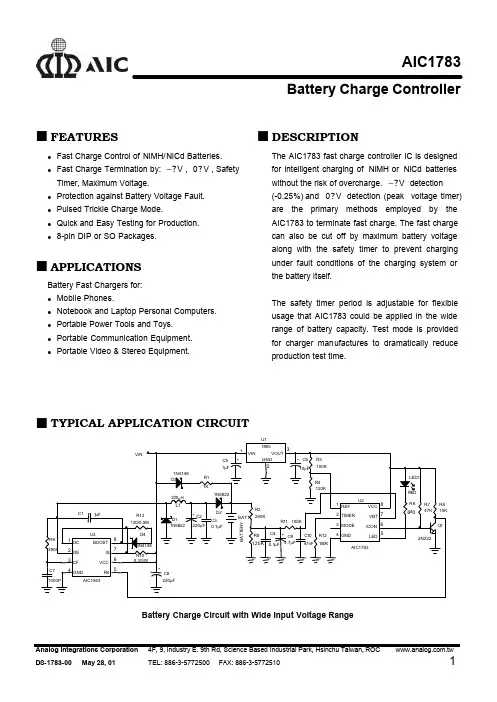
NEC Electronics Inc.CB-C8VX/VM 3-Volt, 0.5-Micron Cell-Based CMOS ASICDescriptionNEC's CB-C8VX/VM CMOS cell-based ASIC family facilitates the design of complete cell-based silicon systems composed of user-defined logic, complex macrofunctions such as microprocessors, intelligent peripherals, analog functions, and compiled memory blocks.The CB-C8VX cell-based ASIC series employs a 0.5-micron (0.35-micron effective) silicon gate CMOS process with silicidation. This advanced process greatly reduces the number of contacts per cell, leading to area-efficient library elements optimized on speed with a 3.3-volt power supply. CB-C8VM, a derivative of CB-C8VX,features a unique I/O structure that provides a full 5-volt CMOS interface. For both technologies, the Titanium-Silicide process results in overall reduced power consumption per cell. Combining very high integration,high speed, and low power consumption, this technology meets today's rigorous application demands.Fully supported by NEC's sophisticated OpenCAD ®design framework, CB-C8VX/VM maximizes design quality and flexibility while minimizing ASIC design time. NEC's OpenCAD system combines popular third-party design tools with proprietary NEC tools,including advanced floorplanner and clock tree synthesis tools.A10985EU1V0DS00April 1996Table 1. CB-C8VX/VM Series Features and BenefitsFigure 1.BGA Package ExamplesOpenCAD is a registered trademark of NEC Electronics Inc.PreliminaryFull 5-Volt CMOS InterfaceCB-C8VM offers a full voltage swing interface to a 5-volt CMOS signal environment. This option is realized by implementing a section of thicker gate oxide into the I/O buffer to guarantee the necessary breakdown voltages.The 5-volt I/O buffers can be placed at any location of the I/O area and are freely mixable with 3.3-volt buffers. The internal core is identical to CB-C8VX.CB-C8VX/VM25-Volt-Tolerant InterfaceCB-C8VX supports both 3.3-volt and 5-volt-tolerant signaling. The 5-volt-tolerant buffers enable CB-C8VX devices to communicate with 5-volt TTL signals while protecting the ASIC. CB-C8VX requires only a 3.3-volt power supply.Integration and PerformanceGate complexities up to 703K usable gates can be integrated on the largest of 36 die sizes, each routable with 2- or 3-metal layers. This gives enough flexibility to optimally fit design needs. Twenty-two die sizes offer a single I/O pad ring and 14 are equipped with a staggered dual pad ring in order to achieve a high pad-to-gate ratio. For details, please refer to Table 2 and Table 3.The family offers an extensive library of primitive macrofunctions characterized for 3.3-volt operation.Each of these blocks has several different drive strengths, allowing the synthesis tool to select the most suitable block for the required internal load. This generally reduces the design overhead without influencing design performance. The internal gate delay for a two-input NAND gate is 110 picoseconds (ps), (F/O=1, L=0mm) and 220 ps under loaded conditions (F/O=2, L=2mm).To meet today's high-speed demands, high-perform-ance I/O macros are mandatory. CB-C8VX/VM supports macros such as GTL and HSTL for fast, low-power data transfer, PLLs to synchronize on-chip system clocks, and PCI signaling standards. Also,CB-C8VX/VM offers a variety of macrofunctions to be incorporated on a single chip. These macrofunctions include CPU cores, peripheral devices, RAM/ROM and analog functions, enabling designers to create systems on silicon.Low Power ConsumptionNEC's CB-C8VX/VM Ti-Silicide process featuresexceptionally low power dissipation to facilitate high-speed operation without the need of costly package options, and drastically increases battery life for hand-held applications. At 3.3-volts, power dissipation for internal cells is 1.04 µW/gate/MHz.Table 2. CB-C8VX/VM Die Steps (124µ pad pitch)Step I/O Max. Usable Gates (1)2 Layer 3 Layer B18881307819617B571041879728195B971202543838156C371363321949828C761524201663023D161685170377555D551846254793820D7519267969101953E1520880484120727E5422493875140813E94240106000159000F34256120969181453F74272136641204961G14288153500230250G53304171234256852G93320183078274617H33336202328303492H72352222219333328J32376254094381141J71392275813413719K11408298797448195K90440347031520547Single pad ring die steps.(1) Glue logic only, with average utilization.Table 3. CB-C8VX/VM Die StepsStep I/O Max. Usable Gates (1)2 Layer 3 Layer B73T 1481884428266C37T 1883025045375C50T 1963270349055D01T 2284400066000D52T 2605704785570D90T 28467797101695E54T 32488281132422F18T 364109125163688F70T 396128875193313G34T 436155297232945H49T 508202766304148J51T 572256047384070K92T 660337531506297M97T788468984703477Dual pad ring die steps.(1) Glue logic only, with average utilization.(80µ staggered pad pitch)3CB-C8VX/VMMulti-Voltage I/O InterfaceFor those systems not yet ready to migrate completely to 3.3-volts, CB-C8 has a full 5-volt CMOS interface available. Applying two additional process steps that realize a "multi-oxide" section in the I/O area, 5-volt speed and drive capabilities are available with the help of a separate 5-volt supply rail. The 5-volt I/O buffers include level shifters to convert the 5-volt signal levels to the internal core supply voltage of 3.3-volts. This CB-C8 derivative is called CB-C8VM and is, except for the different I/O structure, identical to CB-C8VX.For moderate speed and driveable 5-volt I/O cell requirements, CB-C8VM's flexibility provides tolerant I/Os that safely interface to 5V devices using a single 3.3-volt power supply.In both cases, the 3.3-volt and 5-volt interfaces can be mixed without restriction along the entire I/O ring.System on SiliconNEC offers a wide selection of CPU/MCU cores, industry-standard intelligent peripheral macros, and compilable RAM/ROM blocks as well as analog functions in hard macro form that can be integrated onto a single CB-C8VX/VM chip. Including such macrofunctions in an ASIC design makes it possible to achieve a high level of integration, performance, and system security.The range of NEC's on-chip macrofunctions includes NEC's proprietary 32-bit V810™ RISC CPU, and an upgraded high-speed version of the popular 16-bit CPU V30HL™, called V30MX™, which operates at clock speeds of 33 MHz at 3.3-volts, and offers an improved 286-compatible address pipelining and uses a 24-bit address bus. Other specific cores can be implemented on request. For details about the full range of on-chip macrofunctions, refer to Table 4.Embedded macrofunctions are easy to place, route,and simulate. Because these macros are derived from NEC's standard parts, they have fully characterized parameters and can be tested with standard test vectors to ensure full functionality and reliability.NEC's test bus architecture allows complete system simulation, production testing of the internal circuits of the macrofunctions, and seamless embedded CPU core emulation. The CPU may be connected externally and can be replaced by an in-circuit emulator (ICE). All this is performed with only two dedicated test control pins.CB-C8VXCB-C8VM Device Names µPD97xxx µPD99xxx Interface options• true 3.3 V • true 3.3 V • 5 V tolerant• 5 V tolerant • true 5 V CMOSCore voltage 3.3 V 3.3 V I/O voltage3.3 V3.3 V and 5 VTable 4. Macrofunction RangeComparable Macro Device DescriptionNZ 70008H µPD70008A Z80™: 8-bit microprocessor (16 MHz)NZ V30MX µPD70108H V30MX: 16-bit microprocessor (16-bit data bus, 33 MHz)NZ V810µPD70732V810™: 32-bit RISC microprocessor (25 MHz)NZ 71037H µPD71037Programmable DMA controller (4 channels, 20 MHz)NZ 71051H µPD71051USART: serial data control (full-duplex Tx/Rx, 300kbit/s, 20 MHz)NZ 71054H µPD71054Programmable timer/counter (16-bit, 3 counter, 6 modes, 20 MHz)NZ 71055H µPD71055Programmable parallel interface (8-bit, 3 I/O ports, 3 modes)NZ 71059H µPD71059Programmable interrupt control (64 interrupt request inputs)NA 4993µPD49938-bit parallel I/O real-time clockNA 72065BL µPD72065B Single-double density floppy disk controllerNZ 72103µPD72103HDLC Controller: Full duplex, Baud rate 4 Mbps, built-in DMA M I 2C™—I 2C Bus interface: receive, transmit, master and slave NA 16450L NS16C450UART: for PC-compatible serial portsNA 16550LNS16550AUART with FIFO: for PC-compatible serial portsZ80 is a trademark of Zilog, Inc.V30HL, V30MX and v810 are trademarks of NEC Corporation I 2C is a trademark of PhilipsCB-C8VX/VM4Memory MacrosAll memory blocks in NEC's CB-C8VX/VM technology are realized as embedded hard macros and are generated by a memory compiler. To ease the task of RAM testing for the designer, NEC supplies standard test pattern sets, which help to save valuable develop-ment time. NEC offers seven different types of memory blocks, as shown in Table 5.PackagingNEC offers a wide variety of over 60 package types.The CB-C8VX/VM family can be packaged in NEC's most popular surface-mount and through-hole packages. These include plastic quad-flat packs (PQFPs) with up to 376 pins. The QFP range includes thin packages (TQFP, LQFP), QFPs with integrated heatspreader, and tape-automated-bonding QFPs (TAB-QFP) with up to 304 pins. Pin grid arrays (PGAs) with up to 528 pins, BGA packages with up to 672 pins, and TBGA packages with up to 696 pins can be used.CB-C8VX/VM ApplicationsCB-C8VX/VM devices are targeted for 3.3-volt products in telecommunications, electronic data processing (EDP), and consumer applications. Typical telecommunications applications include cellular telephones, high-end pagers, and PCMCIA devices, as well as broad-band communication systems up to 156Mbit/s. In the EDP segment, applications range from personal computers to high-end workstations andTable 5. Memory BlocksMacro TypeWord Range Bit Range Step (Word / Bit)ROM128 - 8192 4 - 64128 / 2256 - 16384 2 - 32256 / 1512 - 32768 1 - 16512 / 1Low-power RAM, single-port64 - 512 1 - 3216 / 1(asynchronous, bi-directional I/O)128 - 1024 1 - 1632 / 1256 - 2048 1 - 864 / 1Low-power RAM, single-port 64 - 512 1 - 3216 / 1(synchronous, separate I/O)128 - 1024 1 - 1632 / 1256 - 2048 1 - 864 / 1High-density RAM, single-port 128 - 2048 1 - 6416 / 1(synchronous, separate I/O)High-speed RAM, single-port 32 - 20481- 3232 / 1(synchronous, separate I/O)Register files, dual-port 8 - 256 4 - 32 4 / 1Register files, triple-port8 - 2564 - 324 / 1mainframes, multimedia platforms, graphic accel-erators, personal digital assistants (PDAs), notebook and pen-based devices, hand-held data terminals, and hard disk controllers. Consumer applications include games, video cameras, portable printers, and sophisticated calculators.Each of these applications demands the benefits of increased integration and low power consumption that only a cell-based family using an optimized 3.3-volt process technology can deliver. CB-C8VX/VM provides the flexibility needed when a 3.3-volt process is required.Design Tool SupportThe CB-C8VX/VM family is fully supported by NEC's OpenCAD Design System, a unified front-to-back-end design package that allows designers to mix and match tools from the industry's most popular third-party vendors and from NEC's offering of powerful propri-etary software tools. These tools perform schematic capture, logic synthesis, floorplanning, logic and timing simulation, layout, design and circuit rule check, and memory compilations.The company's proprietary clock tree synthesis tool automatically buffers clock lines as needed to minimize clock skew, which is essential for half-micron designs.The nonlinear delay calculator ensures timing accuracy throughout the simulation, synthesis, and silicon stages.Finally, NEC's memory compiler software enables memory block generation based on size and perform-ance requirements.5CB-C8VX/VMInput/Output Capacitance (V DD =V I =0 V; f =1 MHz)TerminalSymbol Typ Max Unit Input C IN 1020pF Output C OUT 1020pF I/OC I/O1020pF(1)Values include package pin capacitanceAbsolute Maximum RatingsPower supply voltage, V DD 3.3 V supply –0.5 to +4.6 V 5 V supply –0.5 to +6.0 VI/O voltage, V I /V O 3.3 V interface block –0.5 to +4.6 V and (V I /V O < V DD +0.5 V) 5 V-tolerant block –0.5 to +6.6 V and (V I /V O < V DD +3.0 V) 5 V swing block –0.5 to +6.0 V and (V I /V O < V DD +0.5 V)Latch-up current, I LATCH >1 A (typ)Operating temperature, T OPT –40 to +85°C Storage temperature, T STG–65 to +150°CAC Characteristics (V DD = 3.3 V ± 0.3 V; T J = –40 to +125°C)Parameter Symbol MinTyp MaxUnit Conditions Toggle frequency f TOG480MHzD-F/F; F/O = 2 mmDelay time2-input NAND (F322)t PD 236ps F/O = 1; L = 0 mm t PD 272ps F/O = 2; L = typ Flip-flop (F661)t PD 777ps F/O = 1; L = 0 mm t PD 865ps F/O = 2; L = typ t SETUP 420ps —t HOLD 580ps —Input buffer (FI01)t PD 126ps F/O = 1; L = 0 mm t PD 228ps F/O = 2; L = typ Output buffer (9 mA) 3.3 V t PD 1.24ns C L = 15 pF Output buffer (9 mA) 5 V-tolerant t PD 4.262ns C L = 15 pF Output buffer (6 mA) 5 V-swing t PD 2.698ns C L = 15 pF Output rise time (9 mA)t R 1.88ns C L = 15 pF Output fall time (9 mA)t F1.32nsC L = 15 pFRecommended Operating Conditions (V DD = 3.3 V ± 0.165 V; V CC = 5.0 V ± 0.5 V; T J = –40 to +125°C)3.3 V Interface5 V Tolerant5 V Swing 5 V Swing BlockBlockCMOS Level TTL Level (CB-C8VX/VM)(CB-C8VM)(CB-C8 VM)ParameterSymbol Min Max Min Max Min Max Min Max Unit I/O power supply voltage V DD 3.0 3.6 3.0 3.6 4.5 5.5 4.75 5.25V Junction temperature T J –40+125–40+125–40+125–40+125°C High-level input voltage V IH 2.0V DD 2.0 5.50.7 V DDV DD 2.0V DD V Low-level input voltage V IL 00.800.800.3 V DD 00.8V Positive trigger voltage V P 1.2 2.4 1.2 2.4 1.8 4.0 1.2 2.4V Negative trigger voltage V N 0.6 1.80.6 1.80.6 3.10.6 1.8V Hysteresis voltage V H 0.3 1.50.3 1.50.3 1.50.3 1.5V Input rise/fall time t R , t F 0200020002000200ns Input rise/fall time, Schmittt R , t F10101010msPower ConsumptionDescription Limits Unit Internal gate (1) 1.04µW/MHz Input block —µW/MHz Output block—µW/MHz(1)Assumes 30% internal gate switching at one timeCaution: Exposure to absolute maximum ratings for extended periods may affect device reliability; exceeding the ratings could cause permanent damage. The device should not be operated outside the recommended operating conditions.Caution: Exposure to absolute maximum ratings for extended periods may affect device reliability; exceeding the ratings could cause permanent damage. The device should not be operated outside the recommended operating conditions.CB-C8VX/VM6DC Characteristics (V DD = 3.3 V ± 0.3 V, 5 V ± 0.5 V; T A = –40 to +125°C)ParametersSymbol Conditions MIN.TYP.MAX.Unit Static current consumptionI L V I = V DD B18 to H33200µA or GNDH72 to K90300µA Off-state output current I OZ V O = V DD or GND ±10µA Output short-circuit current I OS V O = 0V–250mAInput leakage currentI INormal inputV I = V DD or GND ±10-5±10µA With pull-up resistor (50 ký)V I = GND –10–40–80µA With pull-up resistor (5 ký)V I = GND –130–350–640µA With pull-down resistor (50 ký)V I = V DD1065130µALow-level output currentI OL3 V interface bufferV OL = 0.4VmA 3 mA I OL 3mA 6 mA I OL 6mA 9 mA I OL 9mA 12 mA I OL 12mA 18 mA I OL 18mA 24 mA I OL24mA 5 V-tolerant bufferV OL = 0.4VmA 1 mA I OL 1mA 2 mA I OL 2mA 3 mA I OL 3mA 6 mA I OL 6mA 9 mA I OL9mA 5 V swing bufferV OL = 0.4VmA 1 mA I OL 1mA 2 mA I OL 2mA 3 mA I OL 3mA 6 mA I OL 6mA 9 mA I OL 9mA 12 mA I OL 12mA 18 mAI OL 18mAHigh-level output currentI OH3 V interface bufferV OH = 2.4V3 mA I OH -3mA 6 mA I OH -6mA 9 mA I OH -9mA 12 mA I OH -12mA 18 mA I OH -18mA 24 mAI OH-24mACB-C8VX/VM DC Characteristics (continued) (V= 3.3 V ± 0.3 V, 5 V ± 0.5 V; T A= –40 to +125°C)DDParameters Symbol Conditions MIN.TYP.MAX.Unit High-level output current I OH5 V-tolerant buffer V OH = 2.4 V1 mA I OH–1mA2 mA I OH–2mA3 mA I OH–3mA6 mA I OH–6mA9 mA I OH–9mA5 V swing buffer V OH = –0.4 V1 mA I OH–1mA2 mA I OH–2mA3 mA I OH–3mA6 mA I OH–6mA9 mA I OH–9mA12 mA I OH–12mA18 mA I OH–18mA Low-level output voltage V OL I OL = 0 mA0.1V3 V interface buffer V OL0.1V5 V interface buffer V OL0.1V5 V swing buffer V OL0.1VHigh-level output voltage V OH I OH = 0 mA V3 V interface buffer V OH V DD–0.1V5 V interface buffer V OH V DD–0.2V5 V swing buffer V OH V DD–0.1V78For literature, call toll-free 7 a.m. to 6 p.m. Pacific time: 1-800-366-9782or FAX your request to: 1-800-729-9288No part of this document may be copied or reproduced in any form or by any means without the prior written consent of NEC Electronics Inc.(NECEL). The information in this document is subject to change without notice. ALL DEVICES SOLD BY NECEL ARE COVERED BY THE PROVISIONS APPEARING IN NECEL TERMS AND CONDITIONS OF SALES ONLY. INCLUDING THE LIMITATION OF LIABILITY, WAR-RANTY, AND PATENT PROVISIONS. NECEL makes no warranty, express, statutory, implied or by description, regarding information set forth herein or regarding the freedom of the described devices from patent infringement. NECEL assumes no responsibility for any errors that may appear in this document. NECEL makes no commitments to update or to keep current information contained in this document. The devices listed in this document are not suitable for use in applications such as, but not limited to, aircraft control systems, aerospace equipment, submarine cables, nuclear reactor control systems and life support systems. “Standard” quality grade devices are recom-mended for computers, office equipment, communication equipment, test and measurement equipment, machine tools, industrial robots,audio and visual equipment, and other consumer products. For automotive and transportation equipment, traffic control systems, anti-disaster and anti-crime systems, it is recommended that the customer contact the responsible NECEL salesperson to determine the reliabilty requirements for any such application and any cost adder. NECEL does not recommend or approve use of any of its products in life support devices or systems or in any application where failure could result in injury or death. If customers wish to use NECEL devices in applications not intended by NECEL, customer must contact the responsible NECEL sales people to determine NECEL’s willingness to support a given application.©1996 NEC Electronics Inc./Printed in U.S.A.Document No. A10985EU1V0DS00NEC ASIC DESIGN CENTERSWEST•3033 Scott Boulevard Santa Clara, CA 95054TEL 408-588-5008FAX 408-588-5017•One Embassy Centre9020 S.W. Washington Square Road,Suite 400Tigard, OR 97223TEL 503-671-0177FAX 503-643-5911THIRD-PARTY DESIGN CENTERSSOUTH CENTRAL/SOUTHEAST•Koos Technical Services, Inc.385 Commerce Way, Suite 101Longwood, FL 32750TEL 407-260-8727FAX 407-260-6227•Integrated Silicon Systems Inc.2222 Chapel Hill Nelson Highway Durham, NC 27713TEL 919-361-5814FAX 919-361-2019•Applied Systems, Inc.1761 W. Hillsboro Blvd., Suite 328Deerfield Beach, FL 33442TEL 305-428-0534FAX 305-428-5906NORTH CENTRAL/NORTHEAST•The Meadows, 2nd Floor 161 Worcester Road Framingham, MA 01701TEL 508-935-2200FAX 508-935-2234•Greenspoint Tower2800 W. Higgins Road, Suite 765Hoffman Estates, IL 60195TEL 708-519-3945FAX 708-882-7564NEC Electronics Inc.CORPORATE HEADQUARTERS2880 Scott Boulevard P.O. Box 58062Santa Clara, CA 95052TEL 408-588-6000SOUTH CENTRAL/SOUTHEAST•16475 Dallas Parkway, Suite 380Dallas, TX 75248TEL 972-735-7444FAX 972-931-8680•Research Triangle Park2000 Regency Parkway, Suite 455Cary, NC 27511TEL 919-460-1890FAX 919-469-5926•Two Chasewood Park 20405 SH 249, Suite 580Houston, TX 77070TEL 713-320-0524FAX 713-320-0574。