DSPIC33F引脚
- 格式:pdf
- 大小:171.32 KB
- 文档页数:1
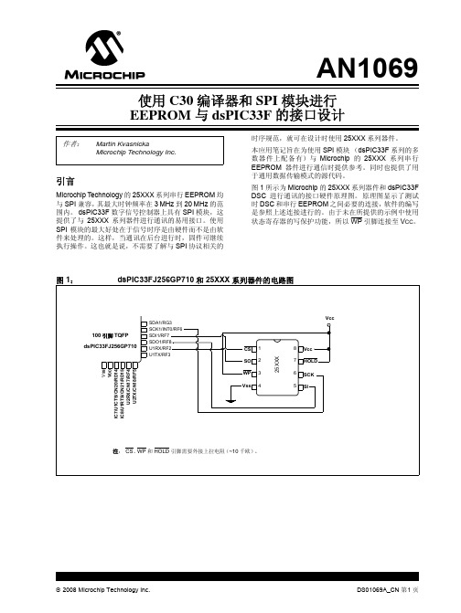
Microchip dsPIC33FJ PSFB砖形DC-DC转换器参考设计关键词:电源管理,DC/DC转换器Microchip 公司的dsPIC33FJ06GS101/X02和dsPIC33FJ16GSX02/X04包括有广泛的DSP功能和高性能16位MCU架构。
3.0-3.6V的性能达到40MIPS,具有16位宽的数据通路,24位宽指令,广泛应用在AC/DC转换器,汽车HID,电池充电器,DC/DC转换器,数字照明,电磁炉,可再生能源/纯正弦波逆变器和UPS。
本文介绍了dsPIC33FJ系列主要特性,方框图和CPU 核方框图,DSP 引擎方框图,数字PFC框图以及多种应用框图。
此外还介绍了相移全桥(PSFB)1/4砖形DC-DC转换器参考设计主要特性和指标,详细电路图与材料清单(BOM)。
dsPIC33FJ06GS101/X02 and dsPIC33FJ16GSX02/X04 devices contain extensive Digital Signal Processor (DSP) functionality with a high-performance, 16-bit microcontroller (MCU) architecture.dsPIC33FJ系列主要特性:Operating Range:• Up to 40 MIPS Operation (at 3.0-3.6V):- Industrial temperature range (-40℃to +85℃)- Extended temperature range (-40℃to +125℃)High-Performance DSC CPU:• Modified Harvard Architecture• C Compiler Optimized Instruction Set• 16-Bit Wide Data Path• 24-Bit Wide Instructions• Linear Program Memory Addressing up to 4M Instruction Words• Linear Data Memory Addressing up to 64 Kbytes• 83 Base Instructions: Mostly 1 Word/1 Cycle• Two 40-Bit Accumulators with Rounding and Saturation Options• Flexible and Powerful Addressing modes:- Indirect- Modulo- Bit-Reversed• Software Stack• 16 x 16 Fractional/Integer Multiply Operations • 32/16 and 16/16 Divide Operatio ns• Single-Cycle Multiply and Accumulate:- Accumulator write back for DSP operations- Dual data fetch• Up to ±16-Bit Shifts for up to 40-Bit Data Digital I/O:• Peripheral Pin Select Functionality• Up to 35 Programmable Digital I/O Pins• Wake-up/Interrupt-on-Change for up to 30 Pins • Output Pins can Drive Voltage from 3.0V to 3.6V • Up to 5V Output with Open-Drain Configuration • 5V Tolerant Digital Input Pins (except RB5)• 16 mA Source/Sink on All PWM pinsOn-Chip Flash and SRAM:• Fl ash Program Memory (up to 16 Kbytes)• Data SRAM (up to 2 Kbytes)• Boot and General Security for Program Flash Peripheral Features:• Timer/Counters, up to Three 16-Bit Timers:- Can pair up to make one 32-bit timer• Input Capture (up to two channe ls):- Capture on up, down or both edges- 16-bit capture input functions- 4-deep FIFO on each capture• Output Compare (up to two channels):- Single or Dual 16-Bit Compare mode- 16-Bit Glitchless PWM mode• 4-Wire SPI:- Framing supports I/O interface to simple codecs- 1-deep FIFO Buffer.- Supports 8-bit and 16-bit data- Supports all serial clock formats and sampling modes • I2C™:- Supports Full Multi-Master Slave mode- 7-bit and 10-bit addressing- Bus collision detection and arbitration- Integrated signal conditioning- Slave address masking• UART:- Interrupt on address bit detect- Interrupt on UART error- Wake-up on Start bit from Sleep mode- 4-character TX and RX FIFO buffers- LIN bus support- IrDA® encoding and decoding in hardware- High-Speed Baud mode- Hardware Flow Control with CTS and RTSInterrupt Controller:• 5-Cycle Latency• Up to 35 Available Interrupt Sources• Up to Three External Interrupts• Seven Programmable Priori ty Levels• Four Processor ExceptionsHigh-Speed PWM Module Features:• Up to Four PWM Generators with Four to Eight Outputs• Individual Time Base and Duty Cycle for each of the Eight PWM Outputs • Dead Time for Rising and Falling Edges• Duty Cycle Resolution of 1.04 ns• Dead-Time Resolution of 1.04 ns• Phase Shift Resolution of 1.04 ns• Frequency Resolution of 1.04 ns• PWM modes Supported:- Standard Edge-Aligned- True Independent Output- Complementary- Center-Aligned- Push-Pull- Multi-Phase- Variable Phase- Fixed Off-Time- Current Reset- Current-Limit• Independent Fault/Current-Limit Inputs for 8 PWM Outputs• Output Override Control• Special Event Trigger• PWM Capture Feature• Prescaler for Input Clock• Dual T rigger from PWM to ADC• PWMxL, PWMxH Output Pin Swapping• PWM4H, PWM4L Pins Remappable• On-the-Fly PWM Frequency, Duty Cycle and Phase Shift Changes • Disabling of Individual PWM Generators• Leading-Edge Blanking (LEB) FunctionalityHigh-Speed Analog Comparator• Up to Four Analog Comparators:- 20 ns response time- 10-bit DAC for each analog comparator- DACOUT pin to provide DAC output- Programmable output polarity- Selectable input source- ADC sample and convert capability• PWM Mod ule Interface:- PWM duty cycle control- PWM period control- PWM Fault detectHigh-Speed 10-Bit ADC• 10-Bit Resolution• Up to 12 Input Channels Grouped into Six Conversion Pairs • Two Internal Reference Monitoring Inputs Grouped into a Pair • S uccessive Approximation Register (SAR)Converters for Parallel Conversions of Analog Pairs:- 4 Msps for devices with two SARs- 2 Msps for devices with one SAR• Dedicated Result Buffer for each Analog Channel• Independent Trigger Source Section for each Analog Input Conversion Pair Power Management:• On-Chip 2.5V Voltage Regulator• Switch between Clock Sources in Real Time• Idle, Sleep, and Doze modes with Fast Wake-upCMOS Flash Technology:• Low-Power, High-Speed Flash Technology• Fully Static Design• 3.3V (±10%) Operating Voltage• Industrial and Extended Temperature• Low-Power ConsumptionSystem Management:• Flexible Clock Options:- External, crystal, resonator, internal RC- Phase-Locked Loop (PLL) with 120 MHz VCO- Primary Crystal Oscillator (OSC) in the range of 3 MHz to 40 MHz- Internal Low-Power RC (LPRC) oscillator at a frequency of 32 kHz- Internal Fast RC (FRC) oscillator at a frequency of 7.37 MHz• Power-on Reset (POR)• Brown-out Reset (BOR)• Power-up Timer (PWRT)• Oscillator Start-up Timer (OST)• Watchdog Timer with its RC Oscillator• Fail-Safe Clock Monitor (FSCM)• Reset by Multiple Sources• In-Circuit Serial Programming™ (ICSP™)• Reference Oscillator OutputdsPIC33FJ 系列应用:• AC-to-DC Converters• Automotive HID• Battery Chargers• DC-to-DC Converters• Digital Lighting• Induction Cooking• LED Ballast• Renewable Power/Pure Sine Wave Inverters • Uninterruptible Power Supply (UPS)图1。

基于dsPIC33F单片机的开关磁阻发电控制系统徐文;朱学忠【摘要】针对高转速运行的12/8结构开关磁阻发电机,构建了一种以dsPIC33F 单片机为主、复杂可编程逻辑器件为辅的控制系统.通过对开关磁阻发电机工作原理和该单片机相关模块的分析及应用,给出了控制系统的硬件设计和主要模块的软件配置及控制流程.最后由调试得到了核心模块的实验波形.实验结果证明,该控制系统可以满足开关磁阻电机高速时发电的需求,整个控制系统设计合理、性能可靠,容易实现系统控制.%Supplemented by a complex programmable logic device, a dsPIC33F microcontroller-based 12/8 structured switched reluctance generator control system with the focus on the operation under high speed was built. And then, with the analysis and application of operating principles of the switched reluctance generator and relevant modules of the said microcontroller, hardware design of the control system, as well as the software configuration and control flow of major modules were proposed. Finally, experiment waveforms of key module were obtained by debugging. The results indicate that the control system was capable and sufficient to meet the needs of the switched reluctance generator during the power generation at a high speed. The design of the entire control system is reasonable and easy to implement, also performing reliably and stably.【期刊名称】《机电工程》【年(卷),期】2012(029)001【总页数】4页(P79-82)【关键词】开关磁阻发电机;输入捕捉;输出比较;控制系统设计【作者】徐文;朱学忠【作者单位】南京航空航天大学自动化学院,江苏南京210016;南京航空航天大学自动化学院,江苏南京210016【正文语种】中文【中图分类】TM352;TM61开关磁阻电机作为调速电动机开发应用已有近30年历史了。

查询DSPIC33FJ12GP201供应商捷多邦,专业PCB打样工厂,24小时加急出货dsPIC33FJ12GP201/202数据手册高性能16位数字信号控制器 2007 Microchip Technology Inc.超前信息DS70264A_CNDS70264A_CN 第ii 页超前信息2007 Microchip Technology Inc.提供本文档的中文版本仅为了便于理解。
请勿忽视文档中包含的英文部分,因为其中提供了有关Microchip 产品性能和使用情况的有用信息。
Microchip Technology Inc.及其分公司和相关公司、各级主管与员工及事务代理机构对译文中可能存在的任何差错不承担任何责任。
建议参考Microchip Technology Inc.的英文原版文档。
本出版物中所述的器件应用信息及其他类似内容仅为您提供便利,它们可能由更新之信息所替代。
确保应用符合技术规范,是您自身应负的责任。
Microchip 对这些信息不作任何明示或暗示、书面或口头、法定或其他形式的声明或担保,包括但不限于针对其使用情况、质量、性能、适销性或特定用途的适用性的声明或担保。
Microchip 对因这些信息及使用这些信息而引起的后果不承担任何责任。
如果将Microchip 器件用于生命维持和/或生命安全应用,一切风险由买方自负。
买方同意在由此引发任何一切伤害、索赔、诉讼或费用时,会维护和保障Microchip 免于承担法律责任,并加以赔偿。
在Microchip 知识产权保护下,不得暗中或以其他方式转让任何许可证。
商标Microchip 的名称和徽标组合、Microchip 徽标、Accuron 、dsPIC 、K EE L OQ 、K EE L OQ 徽标、microID 、MPLAB 、PIC 、PICmicro 、PICSTART 、PRO MATE 、rfPIC 和SmartShunt 均为Microchip Technology Inc.在美国和其他国家或地区的注册商标。
dsPIC30F系列数字信号控制器(DSC)dsPIC30F系列DSC采用程序存储器和数据存储器完全分离的哈佛体系结构:1、CPU结构概述:dsPIC30F的CPU拥有24位指令字。
程序计数器PC为24位宽,最低有效位总是0,除一些特殊指令外,在程序的正常执行中总是忽略其最高有效位,因此程序计数器PC可以寻址4M×24位的用户程序存储器空间。
工作寄存器阵列由16个16位的寄存器构成。
每个工作寄存器都可以充当数据、地址或地址偏移寄存器。
第16个工作寄存器(W15)作为软件堆栈的指针工作,用于中断服务程序和子程序的调用。
dsPIC30F指令集有两类指令:MCU类指令和DSP类指令。
这两类指令无缝地集成到架构中并从同一个执行单元执行。
指令集包括很多寻址模式。
CPU支持固有(无操作数)寻址、相对寻址、立即数寻址、存储器直接寻址、寄存器直接寻址和寄存器间接寻址模式。
每条指令最多支持6种寻址模式。
CPU中包含一个DSP引擎,如图2-2所示,它具备一个高速17位×17位乘法器、一个40位ALU、两个40位饱和累加器和一个40位双向桶形移位寄存器。
该桶形移位寄存器在单个周期内至多可将一个40位的值右移15位或左移16位。
DSP指令可以无缝地与所有其他指令一起操作,其设计可实现最佳的实时性能。
MAC指令和其他相关指令可以同时从存储器中取出两个数据操作数并将两个W寄存器相乘。
这要求数据空间对于这些指令拆分为两块,但对所有其他指令保持线性。
这是通过为每个地址空间指定某些工作寄存器,以透明和灵活的方式实现的。
CPU不支持多级指令流水线,而是利用单级指令预取机制,它在指令执行的前一个周期存取并解码部分指令,以便使可利用的执行时间达到最长。
单周期指令预取机制用来帮助维持吞吐量并提供可预测的执行。
除了改变程序流的指令、双字移动(MOV.D)指令和表指令以外,所有指令都在单个周期内执行。
使用DO和REPEAT 指令支持无开销的程序循环结构,这两个指令在任何时候都可被中断。
微处理器dsPIC33F在微机保护装置中的应用1 引言随着电网供电负荷的日趋加重,电力系统对微机保护装置提出更高要求,一般低档单片机已很难满足设计要求。
近年来,各种集成化的单片DSP的性能得到很大改善,软件和开发工具也越来越多,使得DSP器件及技术更容易使用,价格也能够为广大用户所接受Microchip公司推出的数字信号处理器dsPIC33F集A/D转换、通讯、看门狗、保护和数据存储于一体,同时还支持SPI模式和I2C模式数据传输,便于扩展容量。
因此,开发基于dsPIC33F的微机保护装置,不仅提升保护系统的整体性能和硬件平台的通用性,而且还能缩短开发时间,降低开发及硬件成本,对提高电力系统的稳定运行水平具有一定意义。
2 数字信号控制器dsPIC33F系列简介dsPIC33F系列是高性能16位数字信号控制器,具有扩展的数字信号处理器(DSP)功能和高性能16位微控制器 (MCU)的架构。
它是一种16位改进型哈佛结构RISC器件,融合了高性能16位单片机的控制优势和数字信号处理器的高速运算能力,是一款高性能的数字信号控制器(DSC)。
dsPIC33F系列器件具有以下性能特点:(1)DSP内核和指令系统dsPIC33F的DSP引擎具有1个高速的17位×17位的乘法器,1个40位的ALU,2个40位的饱和累加器以及1个 40位的双向移位器,其运算速度可达40 MI/s,指令字为24位,指令系统包含MCU指令集和DSP指令集。
此外,这些指令对C语言编译器做了专门优化,采用C语言编写的程序代码效率很高。
dsPIC33F允许工作电压±10%的偏差,即工作电压为3.0~3.6 V。
(2)直接存储器访问(DMA)和中断能力dsPIC33F内部集成了8通道直接存储器访问模块,允许CPU执行代码期间在RAM和外设间传输数据,不额外占用周期。
2 KB双端口DMA缓冲区(DMA RAM),用于存储通过DMA传输的数据。
dsPIC33F/PIC24H1.0器件概述本文档定义了dsPIC33F 16位数字信号控制器(Digital Signal Controller,DSC)和PIC24H 16位单片机(MCU)系列的编程规范。
本编程规范仅供为dsPIC33F/ PIC24H系列开发编程支持的人员使用。
仅使用这些器件的客户应该采用支持器件编程的开发工具。
本文档包括下列器件的编程规范:• dsPIC33FJ64GP206• dsPIC33FJ64GP306• dsPIC33FJ64GP310• dsPIC33FJ64GP706• dsPIC33FJ64GP708• dsPIC33FJ64GP710• dsPIC33FJ128GP206• dsPIC33FJ128GP306• dsPIC33FJ128GP310• dsPIC33FJ128GP706• dsPIC33FJ128GP708• dsPIC33FJ128GP710• dsPIC33FJ256GP506• dsPIC33FJ256GP510• dsPIC33FJ256GP710• dsPIC33FJ64MC506• dsPIC33FJ64MC508• dsPIC33FJ64MC510• dsPIC33FJ64MC706• dsPIC33FJ64MC710• dsPIC33FJ128MC506• dsPIC33FJ128MC510• dsPIC33FJ128MC706• dsPIC33FJ128MC708• dsPIC33FJ128MC710• dsPIC33FJ256MC510• dsPIC33FJ256MC710• PIC24HJ64GP206• PIC24HJ64GP210• PIC24HJ64GP506• PIC24HJ64GP510• PIC24HJ128GP206• PIC24HJ128GP210• PIC24HJ128GP306• PIC24HJ128GP310• PIC24HJ128GP506• PIC24HJ128GP510• PIC24HJ256GP206• PIC24HJ256GP210• PIC24HJ256GP6102.0dsPIC33F/PIC24H编程概述在本编程规范中将讨论两种对dsPIC33F/PIC24H系列器件编程的方法。
Microchip dsPIC33F 入门开发方案关键词:DSP,MCU,数字信号控制器,DSC,摘要:Microchip 公司的dsPIC33F系列是高性能16位数字信号控制器,具有扩展的DSP功能和高性能16位微控制器(MCU)的架构。
而DM330011则是dsPIC33F系列的MPLAB入门级开发套件是完整的硬件和软件工具,开发板上内置了调试器,简单安装软件和连接USB电缆到PC,起动MPLAB IDE就能完全控制和运行简单程序,下载和测试你的应用。
本文介绍了dsPIC33F系列的主要性能,方框图以及MPLAB入门级开发套件DM330011的主要性能,开发系统连接图以及完整的电路图。
Microchip 公司的dsPIC33F系列是高性能16位数字信号控制器,具有扩展的DSP功能和高性能16位微控制器(MCU)的架构。
而DM330011则是dsPIC33F系列的MPLAB 入门级开发套件是完整的硬件和软件工具,开发板上内置了调试器,简单安装软件和连接USB电缆到PC,起动MPLAB IDE就能完全控制和运行简单程序,下载和测试你的应用。
本文介绍了dsPIC33F系列的主要性能,方框图以及MPLAB入门级开发套件DM330011的主要性能,开发系统连接图以及完整的电路图。
一.dsPIC33F High-Performance, 16-bit Digital Signal ControllersThe dsPIC33F devices contain extensive Digital Signal Processor (DSP) functionality with a high performance 16-bit microcontroller (MCU) architecture.Operating Range:. Up to 40 MIPS operation (at 3.0-3.6V):- Industrial temperature range (-40°C to +85°C)- Extended temperature range (-40°C to +125°C)High-Performance DSC CPU:. Modified Harvard architecture. C compiler optimized instruction set. 16-bit wide data path. 24-bit wide instructions. Linear program memory addressing up to 4M instruction words. Linear data memory addressing up to 64 Kbytes. 83 base instructions: mostly 1 word/1 cycle. Two 40-bit accumulators with rounding and saturation options. Flexible and powerful addressing modes:- Indirect- Modulo- Bit-Reversed. Software stack. 16 x 16 fractional/integer multiply operations. 32/16 and 16/16 divide operations. Single-cycle multiply and accumulate:- Accumulator write back for DSP operations- Dual data fetch. Up to ±16-bit shifts for up to 40-bit dataDirect Memory Access (DMA):. 8-channel hardware DMA. Up to 2 Kbytes dual ported DMA buffer area (DMA RAM) to store data transferred via DMA:- Allows data transfer between RAM and a peripheral while CPU is executing code (no cycle stealing). Most peripherals support DMATimers/Capture/Compare/PWM:. Timer/Counters, up to five 16-bit timers:- Can pair up to make two 32-bit timers- One timer runs as a Real-Time Clock with an external 32.768 kHz oscillator - Programmable prescaler. Input Capture (up to four channels):- Capture on up, down or both edges- 16-bit capture input functions- 4-deep FIFO on each capture. Output Compare (up to four channels):- Single or Dual 16-bit Compare mode- 16-bit Glitchless PWM mode. Hardware Real-Time Clock/Calendar (RTCC):- Provides clock, calendar, and alarm functionsInterrupt Controller:. 5-cycle latency. 118 interrupt vectors. Up to 49 available interrupt sources. Up to three external interrupts. Seven programmable priority levels. Five processor exceptionsDigital I/O:. Peripheral pin Select functionality. Up to 35 programmable digital I/O pins. Wake-up/Interrupt-on-Change for up to 21 pins. Output pins can drive from 3.0V to 3.6V. Up to 5V output with open drain configuration. All digital input pins are 5V tolerant. 4 mA sink on all I/O pinsOn-Chip Flash and SRAM:. Flash program memory (up to 128 Kbytes). Data SRAM (up to 16 Kbytes). Boot, Secure, and General Security for program FlashSystem Management:. Flexible clock options:- External, crystal, resonator, internal RC- Fully integrated Phase-Locked Loop (PLL)- Extremely low jitter PLL. Power-up Timer. Oscillator Start-up Timer/Stabilizer. Watchdog Timer with its own RC oscillator. Fail-Safe Clock Monitor. Reset by multiple sourcesPower Management:. On-chip 2.5V voltage regulator. Switch between clock sources in real time. Idle, Sleep, and Doze modes with fast wake-upAnalog-to-Digital Converters (ADCs):. 10-bit, 1.1 Msps or 12-bit, 500 Ksps conversion:- Two and four simultaneous samples (10-bit ADC)- Up to 13 input channels with auto-scanning- Conversion start can be manual or synchronized with one of four trigger sources - Conversion possible in Sleep mode- ±2 LSb max integral nonlinearity- ±1 LSb max differential nonlinearityAudio Digital-to-Analog Converter (DAC):. 16-bit Dual Channel DAC module. 100 Ksps maximum sampling rate. Second-Order Digital Delta-Sigma ModulatorData Converter Interface (DCI) module:. Codec interface. Supports I2S and AC.97 protocols. Up to 16-bit data words, up to 16 words per frame. 4-word deep TX and RX buffersComparator Module:. Two analog comparators with programmable input/output configurationCMOS Flash Technology:. Low-power, high-speed Flash technology. Fully static design. 3.3V (±10%) operating voltage. Industrial and Extended temperature. Low power consumptionCommunication Modules:. 4-wire SPI (up to two modules):- Framing supports I/O interface to simple codecs- Supports 8-bit and 16-bit data- Supports all serial clock formats and sampling modes. I2C.:- Full Multi-Master Slave mode support- 7-bit and 10-bit addressing- Bus collision detection and arbitration- Integrated signal conditioning- Slave address masking. UART (up to two modules):- Interrupt on address bit detect- Interrupt on UART error- Wake-up on Start bit from Sleep mode- 4-character TX and RX FIFO buffers- LIN bus support- IrDA® encoding and decoding in hardware- High-Speed Baud mode- Hardware Flow Control with CTS and RTS. Enhanced CAN (ECAN. module) 2.0B active:- Up to eight transmit and up to 32 receive buffers- 16 receive filters and three masks- Loopback, Listen Only and Listen All- Messages modes for diagnostics and bus monitoring- Wake-up on CAN message- Automatic processing of RemoteTransmission Requests- FIFO mode using DMA- DeviceNet. addressing support. Parallel Master Slave Port (PMP/EPSP):- Supports 8-bit or 16-bit data- Supports 16 address lines. Programmable Cyclic Redundancy Check (CRC):- Programmable bit length for the CRC generator polynomial (up to 16-bit length) - 8-deep, 16-bit or 16-deep, 8-bit FIFO for data inputPackaging:. 28-pin SDIP/SOIC/QFN-S. 44-pin TQFP/QFN图1. dsPIC33F DSC框图二.dsPIC33F的MPLAB入门级开发套件DM330011图2.用于dsPIC33F的MPLAB入门级开发套件外形图The MPLAB Starter Kit for dsPIC Digital Signal Controllers is a complete hardware and software tool suite for exploring applications based upon Microchip’s dsPIC DSCs. With a built-in debugger on the board, simply install the software and connect the USB cable to the PC. Start up MPLAB IDE and you are in full control, able to run the sample programs, and to download and test your own applications. The board is designed with dsPIC DSC with 256 KB of flash memory, a high-fidelity audio codec, microphone input and headphone/speaker outputs, and is powered from the USB connection to the PC. Also on the board are reconfigurable switches, potentiometers, a temperature sensor and a 4 Mb serial EEPROM to store data such as audio samples.MPLAB入门级开发套件主要特性:•Board includes integrated debugger / programmer•USB powered•dsPIC33FJ256GP506 DSC with 256 KB Flash and 16 KB RAM•16/24/32 bit codec with a maximum sampling frequency of 48KHz•Low cost audio capture and play back circuitry using the 12 bit ADC and PWM Audio•Microphone and line level inputs with adjustable input gain•100mW headphone amplifier with digital volume control• 2 switches and 3 LEDs for user application purposes• 4 Megabit serial flash memory for application use•Temperature sensor•CD contains MPLAB IDE with full editor, programmer and debugger; MPLAB C Compiler; code examples and user’s guide•All tools provided for developing and prototyping speech and audio application & algorithmsPackage Contents•dsPIC audio board with integrated debugger•MPLAB Starter Kit with CD containing MPLAB IDE, MPLAB C Compiler for dsPIC DSCs, application notes, and sample programs•USB cable图3. MPLAB入门级开发系统连接图图4. MPLAB入门级开发套件方框图图5. 调试输入和控制电路图(1)图6. 调试输入和控制电路图(2)图B 接口/目标电源电路图图8.语音处理电路图图9.闪存存储器电路图图10.输出比较模块 PWM 滤波器电路图图11.音频CODEC 电路图图12.音频输入电路图图13.音频输出电路图图14.用户LED, 用户开关和温度传感器电路图。