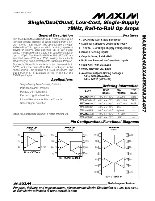
General DescriptionThe MAX4484/MAX4486/MAX4487 single/dual/quad low-cost general-purpose op amps operate from a sin-gle +2.7V to +5.5V supply. The op amps are unity-gain stable with a 7MHz gain-bandwidth product, capable of driving an external 2k Ωload with Rail-to-Rail ®output swing. The amplifiers are stable with capacitive loads of up to 100pF. The MAX4484/MAX4486/MAX4487 are specified from -40°C to +125°C, making them suitable for a variety of harsh environments, such as automotive.The single MAX4484 is available in the ultra-small 5-pin SC70, while the dual MAX4486 is packaged in the space-saving 8-pin SOT23 and µMAX packages. The quad MAX4487 is available in the 14-pin SO and TSSOP packages.________________________ApplicationsSingle-Supply Zero-Crossing Detector Instruments and Terminals Portable Communicators Electronic Ignition ModulesInfrared Receivers for Remote Controls Sensor Signal Detection____________________________Featureso 7MHz Unity-Gain Stable Bandwidth o Stable for Capacitive Loads up to 100pF o +2.7V to +5.5V Single-Supply Voltage Range o Ground-Sensing Inputs o Outputs Swing Rail-to-Railo No Phase Reversal for Overdriven Inputs o 85dB A VOL with 2k ΩLoad o 0.01% THD with 2k ΩLoado Available in Space-Saving Packages5-Pin SC70 (MAX4484)8-Pin SOT23 (MAX4486)MAX4484/MAX4486/MAX4487Single/Dual/Quad, Low-Cost, Single-Supply7MHz, Rail-to-Rail Op Amps________________________________________________________________Maxim Integrated Products1Pin Configurations/Functional Diagrams19-1823, Rev 0; 10/00For price, delivery, and to place orders,please contact Maxim Distribution at 1-888-629-4642,or visit Maxim’s website at .Ordering InformationRail-to-Rail is a registered trademark of Nippon Motorola, Ltd.M A X 4484/M A X 4486/M A X 4487Single/Dual/Quad, Low-Cost, Single-Supply 7MHz, Rail-to-Rail Op AmpsELECTRICAL CHARACTERISTICS—T A = +25°CStresses beyond those listed under “Absolute Maximum Ratings” may cause permanent damage to the device. These are stress ratings only, and functional operation of the device at these or any other conditions beyond those indicated in the operational sections of the specifications is not implied. Exposure to absolute maximum rating conditions for extended periods may affect device reliability.Power Supply Voltage (V DD to V SS ).........................-0.3V to +6V All Other Pins....................................(V SS - 0.3V) to (V DD + 0.3V)Output Short-Circuit Duration (OUT shortedto V DD or V SS )...........................................................Continuous Continuous Power Dissipation (T A = +70°C)5-Pin SC70 (derate 3.1mW/°C above +70°C)..............247mW 5-Pin SOT23 (derate 7.1mW/°C above +70°C) ...........571mW 8-Pin SOT23 (derate 9.1mW/°C above +70°C)............727mW 8-Pin SO (derate 5.88mW/°C above +70°C)................471mW8-Pin µMAX (derate 4.5mW//°C above +70°C)............362mW 14-Pin TSSOP (derate 9.1mW/°C above +70°C).........727mW 14-Pin SO (derate 8.33mW/°C above +70°C)..............667mW Operating Temperature Range .........................-55°C to +125°C Junction Temperature......................................................+150°C Storage Temperature Range.............................-65°C to +150°C Lead Temperature (soldering, 10s).................................+300°CABSOLUTE MAXIMUM RATINGSMAX4484/MAX4486/MAX4487Single/Dual/Quad, Low-Cost, Single-Supply7MHz, Rail-to-Rail Op Amps_______________________________________________________________________________________3ELECTRICAL CHARACTERISTICS —T A = +25°C (continued)(V= +5.0V, V = 0, V = 0, V = V /2, R = ∞to V /2, unless otherwise noted.)Note 1: Guaranteed by design.Note 2:Specifications are 100% tested at T A = +25°C (exceptions marked). All temperature limits are guaranteed by design.ELECTRICAL CHARACTERISTICS —T A = -40°C to +125°CM A X 4484/M A X 4486/M A X 4487Single/Dual/Quad, Low-Cost, Single-Supply 7MHz, Rail-to-Rail Op Amps 4_______________________________________________________________________________________Typical Operating Characteristics(V DD = +5V, V SS = 0, V CM = V DD /2, R L = ∞to V DD /2, unless otherwise noted.)GAIN AND PHASE vs. FREQUENCY (C L = 0)FREQUENCY (Hz)100100k1M10M1k10k100MG A I N (d B ) P H A S E (D E G R E E S )80-200-160-120-80-40400GAIN AND PHASE vs.FREQUENCY WITH CAPACITIVE LOADFREQUENCY (Hz)100100k1M10M1k10k100MG A I N (d B ) P H A S E (D E G R E E S )80-200-160-120-80-4040010100k10M1k10010k1M POWER-SUPPLY REJECTION RATIOvs. FREQUENCYM A X 4484 t o c 03FREQUENCY (Hz)P S R R (d B )-30-20-100-70-60-50-40-80100.51.01.52.02.53.0-40-2020406080100120SUPPLY CURRENT vs. TEMPERATUREM A X 4484 t o c 04TEMPERATURE (°C)C U R R E N T (m A )0.0110.1100101k 10k 10010k1k100k1M10MOUTPUT IMPEDANCE vs. FREQUENCYFREQUENCY (Hz)O U T P U T I M P E D A N C E (Ω)0.20.10.50.40.30.70.80.60.9-402040-206080100120INPUT OFFSET VOLTAGE vs. TEMPERATUREM A X 4484 t o c 06TEMPERATURE (°C)V O S (m V )10152025303540-400-2020406080100120OUTPUT VOLTAGE HIGH vs. TEMPERATURETEMPERATURE (°C)|V D D - V O U T | (m V )024681012-400-2020406080100120OUTPUT VOLTAGE LOW vs. TEMPERATURETEMPERATURE (°C)|V O U T - V S S | (m V )NONINVERTING SMALL- SIGNAL TRANSIENT RESPONSEMAX4484 toc091µs/divINOUT50mV/divMAX4484/MAX4486/MAX4487Single/Dual/Quad, Low-Cost, Single-Supply7MHz, Rail-to-Rail Op Amps_______________________________________________________________________________________5NONINVERTING LARGE-SIGNALTRANSIENT RESPONSEMAX4484 toc10400ns/divINOUT2V/div10152520303540206080100120PERCENT OVERSHOOT vs. CAPACITIVE LOADC LOAD (pF)P E R C E N T O V E R S H O O T (%)40605080701009011010015050200250300LARGE-SIGNAL GAIN vs. OUTPUT VOLTAGE LOW|V OUT - V SS | (mV)G A I N (d B )406050807010090110010015050200250300LARGE-SIGNAL GAIN vs. OUTPUT VOLTAGE HIGH|V DD - V OUT | (mV)G A I N (d B )-60-40-50-20-30-1001001k10k100k1M10M100M CROSSTALK vs. FREQUENCYM A X 4484 t o c 14FREQUENCY (Hz)C R O S S T A L K (d B )-90-70-80607065807585901.0 1.52.0 2.53.0POWER-SUPPLY REJECTION RATIOvs. OPERATING VOLTAGESUPPLY VOLTAGE (V)P S R R (d B )45555040Typical Operating Characteristics (continued)(V DD = +5V, V SS = 0, V CM = V DD /2, R L = ∞to V DD /2, unless otherwise noted.)0.0010.010.110.0110.1101001000TOTAL HARMONIC DISTORTION PLUS NOISE vs. FREQUENCYFREQUENCY (kHz)T H D + N (%)0.040.060.080.100.120.1401.01.50.52.02.53.03.5TOTAL HARMONIC DISTORTION PLUS NOISE vs. AMPLITUDEV IN (Vp-p)T H D + N (%)0.0200.040.060.080.100.120.140 1.0 1.50.5 2.0 2.5 3.0 3.5TOTAL HARMONIC DISTORTION PLUS NOISE vs. AMPLITUDEV IN (Vp-p)T H D + N (%)0.020M A X 4484/M A X 4486/M A X 4487Single/Dual/Quad, Low-Cost, Single-Supply 7MHz, Rail-to-Rail Op Amps 6_______________________________________________________________________________________Detailed DescriptionRail-to-Rail Output StageThe MAX4484/MAX4486/MAX4487 can drive a 2k Ωload and still swing within 50mV of the supply rails.Figure 1 shows the output swing of the MAX4484 con-figured with A V = +1V/V.Driving Capacitive LoadsDriving a capacitive load can cause instability in many op amps, especially those with low quiescent current.The MAX4484/MAX4486/MAX4487 are unity-gain stable for a range of capacitive loads up to 100pF. Figure 2shows the response of the MAX4484 with an excessive capacitive load. Adding a series resistor between the output and the load capacitor (Figure 3) improves the circuit ’s response by isolating the load capacitance from the op amp ’s output.Applications InformationPower Supplies and LayoutThe MAX4484/MAX4486/MAX4487 operates from a sin-gle +2.7V to +5.5V power supply. Bypass the power supply with 0.1µF capacitor to ground.Good layout techniques optimize performance by decreasing the amount of stray capacitance at the op amp ’s inputs and outputs. To decrease stray capaci-tance, minimize trace lengths by placing external com-ponents close to the op amp ’s pins. Use surface-mount components for best results.Pin DescriptionMAX4484/MAX4486/MAX4487Single/Dual/Quad, Low-Cost, Single-Supply7MHz, Rail-to-Rail Op Amps_______________________________________________________________________________________71µs/divFigure 2. Small-Signal Transient Response with Excessive Capacitive Load (C L = 270pF)Figure 1. Rail-to-Rail Output OperationChip InformationTRANSISTOR COUNT:MAX4484: 101MAX4486: 202MAX4487: 404Figure 3. Capacitive-Load-Driving Circuit400µs/divM A X 4484/M A X 4486/M A X 4487Single/Dual/Quad, Low-Cost, Single-Supply 7MHz, Rail-to-Rail Op Amps 8_______________________________________________________________________________________Package InformationMAX4484/MAX4486/MAX4487Single/Dual/Quad, Low-Cost, Single-Supply7MHz, Rail-to-Rail Op Amps_______________________________________________________________________________________9Package Information (continued)M A X 4484/M A X 4486/M A X 4487Single/Dual/Quad, Low-Cost, Single-Supply 7MHz, Rail-to-Rail Op Amps 10______________________________________________________________________________________Package Information (continued)MAX4484/MAX4486/MAX4487Single/Dual/Quad, Low-Cost, Single-Supply7MHz, Rail-to-Rail Op Amps______________________________________________________________________________________11Package Information (continued)M A X 4484/M A X 4486/M A X 4487Single/Dual/Quad, Low-Cost, Single-Supply7MHz, Rail-to-Rail Op AmpsMaxim cannot assume responsibility for use of any circuitry other than circuitry entirely embod ied in a Maxim prod uct. No circuit patent licenses are implied. Maxim reserves the right to change the circuitry and specifications without notice at any time.12____________________Maxim Integrated Products, 120 San Gabriel Drive, Sunnyvale, CA 94086 408-737-7600©2000 Maxim Integrated Products Printed USA is a registered trademark of Maxim Integrated Products.Package Information (continued)。