
08141;中文规格书,Datasheet资料
- 格式:pdf
- 大小:175.63 KB
- 文档页数:2
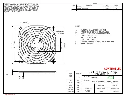

This document was generated on 08/09/2012PLEASE CHECK FOR LATEST PART INFORMATIONPart Number:19221-0483Status:ActiveOverview:Battery Cable LugsDescription:Compression Style Ring Tongue Terminal for 8 AWG Wire, Stud Size 5/16" (M8),Plated, Wide PadDocuments:Drawing (PDF)Product Specification PS-19902-013 (PDF)Product Specification PS-19902-011 (PDF)RoHS Certificate of Compliance (PDF)Agency CertificationCSA LR18689ULE32244GeneralProduct Family Ring and Spade Terminals Series19221CommentsHeavy Duty Crimp Quality Equipment Yes Mil-Spec N/AOverviewBattery Cable Lugs Product Name Battery Cable Lug Type RingUPC800753279131PhysicalBarrel Type Closed InsulationNone Material - Plating Mating Tin Net Weight6.187/g Packaging Type BagPlating min - Mating4.064µm Plating min - Termination 4.064µm Stud Size5/16" (M8)Termination Interface: Style Crimp or Compression Wire Insulation Diameter N/A Wire Size AWG 8Wire Size mm²6.60 - 10.5Material InfoOld Part NumberBCL-8516-WP-PLReference - Drawing NumbersProduct Specification PS-19902-011, PS-19902-013Sales DrawingSD-19221-001, SD-19221-003Seriesimage - Reference onlyEU RoHSChina RoHSELV and RoHS Compliant REACH SVHCContains SVHC: No Low-Halogen Status Not ReviewedNeed more information on product environmental compliance?Email productcompliance@For a multiple part number RoHS Certificate of Compliance, click herePlease visit the Contact Us section for any non-product compliance questions.Search Parts in this Series 19221SeriesApplication Tooling | FAQTooling specifications and manuals are found by selecting the products below.Crimp Height Specifications are then contained in the Application Tooling Specification document.GlobalDescription Product #Hand Crimp Tool 0192840034Putt Pump Dieless Head System0192860065Manual Putt Pump Hydraulic System,Die set required 0192860117Die Set (large) for the HHLS Hydraulic Crimper0192900001Manual tool for Crimping non-insulated 8AWG thru 4/0 Terminals0192940008This document was generated on 08/09/2012PLEASE CHECK FOR LATEST PART INFORMATION分销商库存信息: MOLEX 0192210483。
GS841E18AT/B-180/166/150/130/100256K x 18 Sync Cache Tag 180 MHz–100 MHz3.3 V V DD3.3 V and 2.5 V I/OTQFP, BGACommercial Temp Industrial Temp Features• 3.3 V +10%/–5% core power supply, 2.5 V or 3.3 V I/O supply• Dual Cycle Deselect (DCD)• Intergrated data comparator for Tag RAM application • FT mode pin for flow through or pipeline operation• LBO pin for Linear or Interleave (Pentium TM and X86) Burst mode• Synchronous address, data I/O, and control inputs • Synchronous Data Enable (DE)• Asynchronous Output Enable (OE)• Asynchronous Match Output Enable (MOE)• Byte Write (BWE) and Global Write (GW) operation • Three chip enable signals for easy depth expansion • Internal self-timed write cycle• JTAG Test mode conforms to IEEE standard 1149.1• JEDEC-standard 100-lead TQFP package and 119-BGA • Pb-Free 100-lead TQFP package availableFunctional DescriptionThe GS841E18A is a 256K x 18 high performance synchronous DCD SRAM with integrated Tag RAM comparator. A 2-bit burst counter is included to provide burst interface with Pentium TM and other high performance CPUs. It is designed to be used as a Cache Tag SRAM, as well as data SRAM. Addresses, data IOs, match output, chip enables (CE1, CE2, CE3), address control inputs (ADSP, ADSC, ADV), and write control inputs (BW1, BW2, BWE, GW, DE) are synchronous and are controlled by a positive-edge-triggered clock (CLK).Output Enable (OE), Match Output Enable, and power down control (ZZ) are asynchronous. Burst can be initiated with either ADSP or ADSC inputs. Subsequent burst addresses are generated internally and are controlled by ADV. The burst sequence is either interleave order (Pentium TM or x86) or linear order, and is controlled by LBO.Output registers and the Match output register are provided andcontrolled by the FT mode pin (Pin 14). Through use of the FT mode pin, I/O registers can be programmed to perform pipeline or flow through operation. Flow Through mode reduces latency.Byte write operation is performed by using Byte Write Enable (BWE) input combined with two individual byte write signals BW1-2. In addition, Global Write (GW) is available for writing all bytes at one time.Compare cycles begin as a read cycle with output disabled so that compare data can be loaded into the data input register. Thecomparator compares the read data with the registered input data and a match signal is generated. The match output can be either in Pipeline or Flow Through modes controlled by the FT signal.Low power (Standby mode) is attained through the assertion of the ZZ signal, or by stopping the clock (CLK). Memory data is retained during Standby mode.JTAG boundary scan interface is provided using IEEE standard 1149.1 protocol. Four pins—Test Data In (TDI), Test Data Out(TDO), Test Clock (TCK) and Test Mode Select (TMS)—are used to perform JTAG function.The GS841E18A operates on a 3.3 V power supply and all inputs/outputs are 3.3 V- or 2.5 V-LVTTL-compatible. Separate output (V DDQ ) pins are used to allow both 3.3 V or 2.5 V IO interface.Dual Cycle Deselect (DCD)The GS841E18A is a DCD pipelines synchronous SRAM. DCD SRAMs pipeline disable commands to the same degree as read commands. DCD SRAMs hold the deselect command for one full cycle and then begin turning off their outputs just after the second rising edge of the clock.Parameter Synopsis–180-166-150-133-100Pipeline 3-1-1-1t cycle t KQ I DD 5.5 ns 3.2 ns 335 mA 6.0 ns 3.5 ns 310 mA 6.6 ns 3.8 ns 275 mA 7.5 ns 4.0 ns 250 mA 10 ns 4.5 ns 190 mA Flow Through 2-1-1-1t KQ t cycle I DD8 ns 9.1 ns 210 mA8.5 ns 10 ns 190 mA10 ns 10 ns 190 mA11 ns 15 ns 140 mA12 ns 15 ns 140 mAGS841E18AT/B-180/166/150/130/100Pin Configuration (Package T)807978777675747372717069686766656463626160595857565554535251123456789101112131415161718192021222324252627282930V DDQ V SS D DQ V SS V DDQ DQ DQ V DD NC V SS DQ DQ V DDQ V SS DQ DQ DQ P V SS V DDQ V DDQ V SS DQ DQ V SS VDDQ DQ DQ V SS NC V DD ZZ DQ DQ V DDQ V SS DQ DQ V SS V DDQL B O A A A A A 1A 0T M S T D I V S SV D DT D O T C K A A A A A AA A C E 1C E 2 N C N C B W 2B W 1C E 3C L K G W B W E VD DV S SO E A D S C A D S P A D V A AA 256K x 18Top View DQ P A NC NC NC NC NC DE MATCHMOENC NC NC NC NC NC NCNC NC 100999897969594939291908988878685848382813132333435363738394041424344454647484950FTGS841E18AT/B-180/166/150/130/100 GS841E18A PadOut—119-Bump BGA—Top View (Package B)1234567A V DDQ A A ADSP A A V DDQB NC E2A ADSC A E3NCC NC A A V DD A A NCD DQ B NC V SS NC V SS DQ P NCE NC DQ B V SS E1V SS NC DQ AF V DDQ NC V SSG V SS DQ A V DDQG NC D Q B B B ADV NC NC DQ AH DQ B N C V SS GW V SS DQ A NCJ V DDQ V DD NC V DD NC V DD V DDQK NC DQ B V SS CK V SS NC DQ AL DQ B NC NC NC B A DQ A NCM V DDQ DQ B V SS BW V SS MATCH V DDQN DQ B NC V SS A1V SS DQ A DEP NC DQ P V SS A0V SS MOE DQ AR NC A LBO V DD FT A NCT NC A A NC A A ZZU V DDQ TMS TDI TCK TDO NC V DDQGS841E18AT/B-180/166/150/130/100TQFP Pin DescriptionSymbol DescriptionAn Address Input Signals—Inputs are registered and must meet setup and hold times, as specified onpage 11.CLK Clock Input SignalBWE Byte Write Enable Signal—The byte write enable signal needs to be combined with one of the fourbyte write signals for a write operation to occur.BW1Byte Write signal for data outputs 1 thru 8BW2Byte Write signal for data outputs 9 thru 16GW Global Write EnableCE1,CE2, CE3Chip EnablesOE Output EnableADV Burst address advanceADSP, ADSC Address status signalsDQ Data Input and Output pinsDQP Parity Input and Output pinsMATCH Match OutputMOE Match Output EnableDE Data Enable—Data input registers are updated only when DE is active.ZZ Power down control—Application of ZZ will result in a low standby power consumption.FT Flow Through or Pipeline modeLBO Linear Order Burst modeTMS Test Mode SelectTDI Test Data InTDO Test Data OutTCK Test ClockV DD 3.3 V power supplyV SS GroundV DDQ 2.5 V/3.3 V output power supplyNC No ConnectGS841E18AT/B-180/166/150/130/100PBGA Pin DescriptionSymbol DescriptionAn Address Input Signals—Inputs are registered and must meet setup and hold times, as specified onpage 11.CLK Clock Input SignalBWE Byte Write Enable Signal—The byte write enable signal needs to be combined with one of the fourbyte write signals for a write operation to occur.BW1Byte Write signal for data outputs 1 thru 8BW2Byte Write signal for data outputs 9 thru 16GW Global Write EnableCE1,CE2, CE3Chip EnablesOE Output EnableADV Burst address advanceADSP, ADSC Address status signalsDQ Data Input and Output pinsDQP Parity Input and Output pinsMATCH Match OutputMOE Match Output EnableDE Data Enable—Data input registers are updated only when DE is active.ZZ Power down control—Application of ZZ will result in a low standby power consumption.FT Flow Through or Pipeline modeLBO Linear Order Burst modeTMS Test Mode SelectTDI Test Data InTDO Test Data OutTCK Test ClockV DD 3.3 V power supplyV SS GroundV DDQ 2.5 V/3.3 V output power supplyNC No ConnectGS841E18AT/B-180/166/150/130/100Functional Block DiagramA1A0A0A1D0D1Q1Q0B INARY C OUNTERLoadD QR EGISTE RD QRegister D QRegister D QRegister D QRegister D QRegister DQRegisterDQRegisterA0-17LBO ADV CLK ADSC ADSPGW BWE BW1BW2CE1CE2CE3FTDQ1-16OE ZZPowerdown Control256K X 18Memory Array18181818218AQDDQP1-2DEDQRegisterMatchTAP ControllerInstruction Reg.ID Reg.Bypass Reg Boundary Scan Registers 54TCKTMS TDIA, DQ, ControlTDOMOE always (Ø)GS841E18AT/B-180/166/150/130/100Mode Pin FunctionLBOFunctionL Linear Burst H or NCInterleaved BurstFTFunctionL Flow Through H or NCPipelinePower Down ControlNote:There are pull up devices on LBO and FT pins and pull down device on ZZ pin, so those input pins can be unconnected and the chip will operate in the default states as specified in the above tables.ZZFunctionL or NC Active HStandby, IDD = ISBLinear Burst SequenceA[1:0]A[1:0]A[1:0]A[1:0]1st address 000110112nd address 011011003rd address 101100014th address11000110Interleaved Burst SequenceA[1:0]A[1:0]A[1:0]A[1:0]1st address 000110112nd address 010011103rd address 101100014th address11100100Note: H = logic high, L = logic low, NC = no connectByte Write FunctionFunctionGWBWEBW1BW2Read H H X X Read H L H H Write all bytes L X X X Write all bytes H L L L Write byte 1H L L H Write byte 2HLHLGS841E18AT/B-180/166/150/130/100Notes:1.X means “don’t care,” H means “logic high,” L means “logic low.”2.Write is the logic function of GW, BWE, BW1, BW2. See Byte Write Function table for detail.3.All inputs, except OE, must meet setup and hold on rising edge of CLK.4.Suspending busrt generates a wait cycle.5.ADSP LOW along with SRAM being selected always initiates a Read cycle at the L-H edge of the clock (CLK).6.A Write cycle can only be performed by setting Write low for the clock L-H edge of the subsequent wait cycle. Refer to page 12 for the Write timing diagram.Synchronous Truth TableOperationAddress UsedCE1CE2CE3ADSP ADSC ADV Write OE CLK DQ Deselect Cycle, Power Down none H X X X L X X X L-H High-Z Deselect Cycle, Power Down none L L X L X X X X L-H High-Z Deselect Cycle, Power Down none L X H L X X X X L-H High-Z Deselect Cycle, Power Down none L L X H L X X X L-H High-Z Deselect Cycle, Power Down none L X H H L X X X L-H High-Z Read Cycle, Begin Burst external L H L L X X X L L-H Q Read Cycle, Begin Burst external L H L L X X X H L-H High-Z Read Cycle, Begin Burst external L H L H L X H L L-H Q Read Cycle, Begin Burst external L H L H L X H H L-H High-Z Write Cycle, Begin Burst external L H L H L X L X L-H D Read Cycle, Continue Burst next X X X H H L H L L-H Q Read Cycle, Continue Burst next X X X H H L H H L-H High-Z Read Cycle, Continue Burst next H X X X H L H L L-H Q Read Cycle, Continue Burst next H X X X H L H H L-H High-Z Write Cycle, Continue Burst next X X X H H L L X L-H D Write Cycle, Continue Burst next H X X X H L L X L-H D Read Cycle, Suspend Burst current X X X H H H H L L-H Q Read Cycle, Suspend Burst current X X X H H H H H L-H High-Z Read Cycle, Suspend Burst current H X X X H H H L L-H Q Read Cycle, Suspend Burst current H X X X H H H H L-H High-Z Write Cycle, Suspend Burst current X X X H H H L X L-H D Write Cycle, Suspend BurstcurrentHXXXHHLXL-HDGS841E18AT/B-180/166/150/130/100Notes:1.X means “don’t care,” H means “logic high,” L means “logic low.”2.Write is the logic function of GW, BWE, BW1, BW2. See Byte Write Function table for detail.3.CE is defined as CE1=L, CE2=H and CE3=L4.All signals are synchronous and are sampled by CLK except OE and MOE. OE and MOE are asynchronous and drive the bus immediately.)Note:Permanent damage to the device may occur if the Absolute Maximun Ratings are exceeded. Functional operation should be restricted to the recommended operation conditions. Exposure to higher than recommended voltages, for an extended period of time, could effect the performance and reliability of this component.Truth Table For Read/Write/Compare/Fill Write OperationCEWriteDEMOEOEMatchDQRead L H X X L —Q Write L L L X H —D Compare L H L L H Data Out D Fill Write L L H X X —X Match Deselect H X X L X High High Z DeselectHXXHXHigh ZHigh ZAbsolute Maximum Ratings (Voltage reference to V SS = 0 V)SymbolDescriptionCommericalUnitV DD Supply Voltage –0.5 to 4.6V V DDQ Output Supply Voltage –0.5 to V DD V V CLK CLK Input Voltage –0.5 to 6V V in Input Voltage –0.5 to V DD + 0.5 (≤ 4.6 V max. )V V out Output Voltage –0.5 to V DD + 0.5 (≤ 4.6 V max. )V I out Output Current per I/O +/–20mA P D Power Dissipation 1.5WT OPR Operating Temperature 0 to 70o C T STGStorage Temperature–55 to 125oCGS841E18AT/B-180/166/150/130/100Notes:1.Junction temperature is a function of SRAM power dissapation, package thermal resistance, mounting board temperature, ambient. Temperature air flow, board density, and PCB thermal resistance.2.SCMI G-38-87.3.Average thermal resistance between die and top surface, MIL SPEC-883, Method 1012.1.Package Thermal CharacteristicsRatingLayer BoardSymbolTQFP maxPBGA maxUnitNotesJunction to Ambient (at 200 lfm)single R ΘJA 3228°C/W 1,2Junction to Ambient (at 200 lfm)four R ΘJA 2018°C/W 1,2Junction to Case (TOP)—R ΘJC74°C/W3Notes: 1.Include scope and jig capacitance.2.Test conditions as specified with output loading as shown in Fig. 1 unless otherwise noted.3.Output load 2 for t LZ , t HZ , t OLZ and t OHZ .4.Device is deselected as defined by the Truth Table.AC Test Conditions(VDD = 3.135 V–3.6 V, Ta = 0–70°C)ParameterConditionsInput high level V IH = 2.3 V Input low level V IL = 0.2 V Input slew rate TR = 1 V/ns Input reference level 1.25 V Output reference level1.25 V Output loadFig. 1& 2DQVT = 1.25 V50W 30pF 1DQ2.5 V F IG . 1Output load 1Output load 2F IG . 2225W 225W5pF 1GS841E18AT/B-180/166/150/130/100DC Characteristics and Supply Currents(Voltage reference to V SS = 0 V)(VDD = 3.135 V–3.6 V, Ta = 0–70°C for Commercial Temperature Offering)Parameter Symbol Test Conditions Min MaxInput Leakage Current(except ZZ, FT, LBO pins)I IL V IN = 0 to V DD–1 uA 1 uAZZ Input Current Iin ZZ V DD ≥V IN ≥V IH0 V≤ V IN ≤ V IH–1 uA–1 uA1 uA300 uAMode Input Current (FT & LBO pins)Iin MV DD ≥V IN ≥V IL0 V≤ V IN ≤ V IL–30 0uA–1 uA1 uA1 uAOutput Leakage Current I ol Output Disable,V OUT = 0 to V DD–1 uA 1 uAOutput High Voltage V OH I OH = –4 mA, V DDQ = 2.375 V 1.7 VOutput High Voltage V OH I OH = –4 mA, V DDQ = 3.135 V 2.4 VOutput Low Voltage V OL I OL = +4 mA0.4 VGS841E18AT/B-180/166/150/130/100Operating CurrentsParameter Test Conditions Symbol-180-166-150-133-100Unit 0to70°C–40to85°Cto70°C–40to+85°Cto70°C–40to+85°Cto70°C–40to+85°Cto70°C–40to+85°CO perating Current Device Selected;All other inputs≥ V IH O r ≤ V ILOutput openI DDPipeline335345310320275285250260190200mAI DDFlowThrough210220190200190200140150140150mAStandby Current ZZ≥ V DD – 0.2 VI SBPipeline20303040304030403040mAI SBFlowThrough20303040304030403040mADeselect Supply Current Device Deselected;All other inputs≥ V IH OR≤ V ILI DDPipeline55651101201051151001108090mAI DDFlowThrough40508090809065756575mAGS841E18AT/B-180/166/150/130/100Notes:1.These parameters are sampled and are not 100% tested2.ZZ is an asynchronous signal. However, in order to be recognized on any given clock cycle, ZZ must meet the specified setup and holdtimes as specified above.AC Electrical CharacteristicsParameterSymbol-180-166-150-133-100UnitMinMaxMinMaxMinMaxMinMaxMinMaxPipelineClock Cycle Time tKC 5.5— 6.0— 6.7—7.5—10—ns Clock to Output Valid tKQ — 3.2— 3.5— 3.8—4— 4.5ns Clock to Output InvalidtKQX 1.5— 1.5— 1.5— 1.5— 1.5—ns Clock to Output in Low-Z tLZ 1 1.5— 1.5— 1.5— 1.5— 1.5—ns Clock to Match Valid tKM — 3.2— 3.5— 3.8—4— 4.5ns Clock to Match Invalid tKMX 1.5— 1.5— 1.5— 1.5— 1.5—ns Clock to Match in Low-Z tMLZ 1 1.5— 1.5— 1.5— 1.5— 1.5—ns Flow ThroughClock Cycle Time tKC 9.1—10.0—10.0—15.0—15.0—ns Clock to Output Valid tKQ —8.0—8.5—10.0—11.0—12.0ns Clock to Output InvalidtKQX 3.0— 3.0— 3.0— 3.0— 3.0—ns Clock to Output in Low-Z tLZ 1 3.0— 3.0— 3.0— 3.0— 3.0—ns Clock to Match Valid tKM —8.5—8.5—10.0—11.0—12.0ns Clock to Match Invalid tKMX 3.0— 3.0— 3.0— 3.0— 3.0—ns Clock to Match in Low-Z tMLZ 1 3.0— 3.0— 3.0— 3.0— 3.0—ns Clock HIGH Time tKH 1.3— 1.3— 1.5— 1.7—2—ns Clock LOW Time tKL 1.5— 1.5— 1.7—1.9—2.2—ns Clock to Output in High-Z tHZ 1 1.53.2 1.5 3.5 1.5 3.8 1.54 1.55ns OE to Output Valid tOE — 3.2— 3.5— 3.8—4—5ns OE to output in Low-Z tOLZ 10—0—0—0—0—ns OE to output in High-Z tOHZ 1— 3.2— 3.5— 3.8—4—5ns MOE to Match Valid tMOE — 3.2— 3.5— 3.8—4—5ns MOE to Match in Low-Z tMOLZ 10—0—0—0—0—ns MOE to Match in High-ZtMOHZ 1— 3.2— 3.5— 3.8—4—5ns Setup time tS 1.5— 1.5— 1.5— 2.0— 2.0—ns Hold time tH 0.5—0.5—0.5—0.5—0.5—ns ZZ setup time tZZS 25—5—5—5—5—ns ZZ hold time tZZH 21—1—1—1—1—ns ZZ recoverytZZR20—20—20—20—20—nsGS841E18AT/B-180/166/150/130/100Pipeline Mode TimingBegin Read A Cont Deselect Deselect Write BRead C Read C+1Read C+2Read C+3Cont Deselect DeselecttHZtKQXtKQtLZtHtStOHZtOEtHtStHtStHtStH tStHtStStHtStHtStHtStKCtKL tKHQ(A)D(B)Q(C)Q(C+1)Q(C+2)Q(C+3)ABCHi-ZDeselected with E1E2 and E3 only sampled with ADSCADSC initiated readCK ADSPADSCADVAo–AnGWBWBa–BdE1E2E3GDQa–DQdGS841E18AT/B-180/166/150/130/100Flow Through Mode TimingBegin Read A ContDeselect Write B Read C Read C+1Read C+2Read C+3Read C DeselecttHZtKQX tLZtH tStOHZtOE tKQtHtS tHtS tHtStH tStHtS tHtStHtS tHtS tH tStH tS tHtS tKCtKL tKHABCQ(A)D(B)Q(C)Q(C+1)Q(C+2)Q(C+3)Q(C)E2 and E3 only sampled with ADSP and ADSCE1 masks ADSPADSC initiated readDeselected with E1E1 masks ADSPFixed HighCK ADSPADSCADVAo–AnGWBWBa–BdE1E2E3GDQa–DQdGS841E18AT/B-180/166/150/130/100Pipeline Compare Fill Write CycleHit Miss Fill WriteA BBA A tKMtKMtKMXtKM tMOE tMLZtH tStH tStH tStH tStH tSKAddressDQCEW GDE MOEMatchGS841E18AT/B-180/166/150/130/100Flow Through Compare Fill Write CycleHit Miss Fill WriteA BBA A tKMtKM tKMXtKM tMOE tMLZtH tStH tStH tStH tStH tSKAddressDQCEW GDE MOEMatchGS841E18AT/B-180/166/150/130/100TQFP Package Drawing (Package T)D1D E1EPin 1be cLL1A2A1YθNotes:1.All dimensions are in millimeters (mm).2.Package width and length do not include mold protrusion.SymbolDescriptionMin.Nom.MaxA1Standoff 0.050.100.15A2Body Thickness 1.35 1.40 1.45b Lead Width 0.200.300.40c Lead Thickness 0.09—0.20D Terminal Dimension 21.922.022.1D1Package Body 19.920.020.1E Terminal Dimension 15.916.016.1E1Package Body 13.914.014.1e Lead Pitch —0.65—L Foot Length 0.450.600.75L1Lead Length —1.00—Y Coplanarity 0.10θLead Angle0°—7°GS841E18AT/B-180/166/150/130/100Package Dimensions—119-Bump FPBGA (Package B, Variation 2)A B C D E F G H J K L M N P R T U1 2 3 4 5 6 77 6 5 4 3 2 1A1 TOP VIEWA1 BOTTOM VIEW 1.277.621.2720.3214±0.1022±0.10BA 0.20(4x)Ø0.10Ø0.30CC A B S S Ø0.60~0.90 (119x)CSEATING PLANE0.15C0.50~0.701.86.±0.130.70±0.050.15CA B C D E F G H J K L M N P R T U0.56±0.05S SGS841E18AT/B-180/166/150/130/100 Ordering InformationOrg Part Number1Type Package Speed 2(MHz/ns)T A3Status256K x 18GS841E18AT-180DCD Pipeline/Flow Through TQFP180/8C256K x 18GS841E18AT-166DCD Pipeline/Flow Through TQFP166/8.5C256K x 18GS841E18AT-150DCD Pipeline/Flow Through TQFP150/10C256K x 18GS841E18AT-133DCD Pipeline/Flow Through TQFP133/11C256K x 18GS841E18AT-100DCD Pipeline/Flow Through TQFP100/12C256K x 18GS841E18AT-180I DCD Pipeline/Flow Through TQFP180/8I256K x 18GS841E18AT-166I DCD Pipeline/Flow Through TQFP166/8.5I256K x 18GS841E18AT-150I DCD Pipeline/Flow Through TQFP150/10I256K x 18GS841E18AT-133I DCD Pipeline/Flow Through TQFP133/11I256K x 18GS841E18AT-100I DCD Pipeline/Flow Through TQFP100/12I256K x 18GS841E18AGT-180DCD Pipeline/Flow Through Pb-Free TQFP180/8C256K x 18GS841E18AGT-166DCD Pipeline/Flow Through Pb-Free TQFP166/8.5C256K x 18GS841E18AGT-150DCD Pipeline/Flow Through Pb-Free TQFP150/10C256K x 18GS841E18AGT-133DCD Pipeline/Flow Through Pb-Free TQFP133/11C256K x 18GS841E18AGT-100DCD Pipeline/Flow Through Pb-Free TQFP100/12C256K x 18GS841E18AGT-180I DCD Pipeline/Flow Through Pb-Free TQFP180/8I256K x 18GS841E18AGT-166I DCD Pipeline/Flow Through Pb-Free TQFP166/8.5I256K x 18GS841E18AGT-150I DCD Pipeline/Flow Through Pb-Free TQFP150/10I256K x 18GS841E18AGT-133I DCD Pipeline/Flow Through Pb-Free TQFP133/11I256K x 18GS841E18AGT-100I DCD Pipeline/Flow Through Pb-Free TQFP100/12I256K x 18GS841E18AB-180DCD Pipeline/Flow Through119 BGA (var. 2)180/8C256K x 18GS841E18AB-166DCD Pipeline/Flow Through119 BGA (var. 2)166/8.5C256K x 18GS841E18AB-150DCD Pipeline/Flow Through119 BGA (var. 2)150/10C256K x 18GS841E18AB-133DCD Pipeline/Flow Through119 BGA (var. 2)133/11C256K x 18GS841E18AB-100DCD Pipeline/Flow Through119 BGA (var. 2)100/12C256K x 18GS841E18AB-180I DCD Pipeline/Flow Through119 BGA (var. 2)180/8I256K x 18GS841E18AB-166I DCD Pipeline/Flow Through119 BGA (var. 2)166/8.5I256K x 18GS841E18AB-150I DCD Pipeline/Flow Through119 BGA (var. 2)150/10I256K x 18GS841E18AI-133I DCD Pipeline/Flow Through119 BGA (var. 2)133/11I256K x 18GS841E18AB-100I DCD Pipeline/Flow Through119 BGA (var. 2)100/12INotes:1.Customers requiring delivery in Tape and Reel should add the character “T” to the end of the part number. Example: GS841E18AT-166T.2.The speed column indicates the cycle frequency (Mhz) of the device in Pipelined mode and the latency (ns) in Flow Through mode. Eachdevice is Pipeline / Flow through mode selectable by the user.3.T A = C = Commercial Temperature Range. T A = I = Industrial Temperature Range.4. GSI offers other versions this type of device in many different configurations and with a variety of different features, only some of whichare covered in this data sheet. See the GSI Technology web site for a complete listing of current offerings.GS841E18AT/B-180/166/150/130/100Specifications cited are subject to change without notice. For latest documentation see .Rev: 1.03 4/200521/21© 2001, GSI Technology 4Mb Synchronous Tag RAM Datasheet Revision History Rev. Code: Old;NewTypes of Changes Format or Content Page /Revisions;Reason GS841E18A_r1• Creation of new datasheet GS841E18A_r1;GS841E18A_r1_01Content • Moved TCK from U6 (incorrect placement) to U4 (correct placement) on BGA• Changed U6 to NCGS841E18A_r1_01; GS841E18A_r1_02Format/Content • Updated format• Added 180 MHz speed bin• Updated timing diagrams• Updated mechanical drawings• Added Pb-Free info for TQFPGS841E18A_r1_02;GS841E18A_r1_03Content• Added Pipeline Compare Fill Write Cycle and Flow ThroughCompare Fill Write Cycle timing diagrams 元器件交易网。
FDS89141 Dual N-Channel PowerTrench ® MOSFETPin 1SO-8D1D1D2D2S2S1G1MOSFET Maximum RatingsFDS89141 Dual N-Channel PowerTrench ® MOSFETElectrical Characteristics T J = 25°C unless otherwise noted Off CharacteristicsOn CharacteristicsDynamic CharacteristicsSwitching CharacteristicsDrain-Source Diode CharacteristicsSymbolParameterTest ConditionsMinTypMaxUnitsBV DSS Drain to Source Breakdown Voltage I D = 250 μA, V GS = 0 V100 V ΔBV DSS ΔT J Breakdown Voltage Temperature CoefficientI D = 250 μA, referenced to 25 °C69mV/°C I DSS Zero Gate Voltage Drain Current V DS = 80 V, V GS = 0 V 1μA I GSSGate to Source Leakage CurrentV GS = ±20 V, V DS = 0 V±100nAV GS(th)Gate to Source Threshold Voltage V GS = V DS , I D = 250 μA 2 3.14V ΔV GS(th) ΔT J Gate to Source Threshold Voltage Temperature CoefficientI D = 250 μA, referenced to 25 °C -9 mV/°Cr DS(on)Static Drain to Source On Resistance V GS = 10 V, I D = 3.5 A4762m ΩV GS = 6 V, I D = 2.8 A63100V GS = 10 V, I D = 3.5 A, T J = 125 °C 81107g FSForward TransconductanceV DS = 10 V, I D = 3.5 A14.7S C iss Input Capacitance V DS = 50 V, V GS = 0 V,f = 1MHz299398pF C oss Output Capacitance7093pF C rss Reverse Transfer Capacitance4.77pF R gGate Resistance1.0Ωt d(on)Turn-On Delay Time V DD = 50 V, I D = 3.5 A,V GS = 10 V, R GEN = 6 Ω510ns t r Rise Time1.410ns t d(off)Turn-Off Delay Time9.820ns t f Fall Time2.210ns Q g(TOT)Total Gate Charge V GS = 0 V to 10 V V DD = 50 V, I D =3.5 A5.17.1nC Q g(TOT)Total Gate Charge V GS = 0 V to 5 V2.94.1nC Q gs Gate to Source Charge 1.4nC Q gdGate to Drain “Miller” Charge1.3nCV SD Source to Drain Diode Forward Voltage V GS = 0 V, I S = 3.5 A (Note 2)0.8 1.3V V GS = 0 V, I S = 2 A (Note 2)0.81.2t rr Reverse Recovery Time I F = 3.5 A, di/dt = 100 A/μs3353ns Q rrReverse Recovery Charge2337nCNOTES:1. R θJA is determined with the device mounted on a 1in 2 pad 2 oz copper pad on a 1.5 x 1.5 in. board of FR-4 material. R θJC is guaranteed by design while R θCA is determined by the user's board design.2. Pulse Test: Pulse Width < 300μs, Duty cycle < 2.0%.3. Starting T J = 25°C, L = 3.0 mH, I AS = 5.0 A, V DD = 100 V, V GS = 10V.b) 135°C/W when mounted on a minimun pada) 78°C/W whenmounted on a 1 in 2 pad of 2 oz copperMOSFETMOSFETMOSFETFDS89141 Dual N-Channel PowerTrench ® MOSFET*Trademarks of System General Corporation, used under license by Fairchild Semiconductor.DISCLAIMERFAIRCHILD SEMICONDUCTOR RESERVES THE RIGHT TO MAKE CHANGES WITHOUT FURTHER NOTICE TO ANY PRODUCTS HEREIN TO IMPROVE RELIABILITY, FUNCTION, OR DESIGN. FAIRCHILD DOES NOT ASSUME ANY LIABILITY ARISING OUT OF THE APPLICATION OR USE OF ANY PRODUCT OR CIRCUIT DESCRIBED HEREIN; NEITHER DOES IT CONVEY ANY LICENSE UNDER ITS PATENT RIGHTS, NOR THE RIGHTS OF OTHERS. THESE SPECIFICATIONS DO NOT EXPAND THE TERMS OF FAIRCHILD’S WORLDWIDE TERMS AND CONDITIONS, SPECIFICALLY THE WARRANTY THEREIN, WHICH COVERS THESE PRODUCTS.LIFE SUPPORT POLICYFAIRCHILD’S PRODUCTS ARE NOT AUTHORIZED FOR USE AS CRITICAL COMPONENTS IN LIFE SUPPORT DEVICES OR SYSTEMS WITHOUT THE EXPRESS WRITTEN APPROVAL OF FAIRCHILD SEMICONDUCTOR CORPORATION.As used here in:1. Life support devices or systems are devices or systems which, (a) areintended for surgical implant into the body or (b) support or sustain life, and (c) whose failure to perform when properly used in accordance with instructions for use provided in the labeling, can be reasonably expected to result in a significant injury of the user.2.A critical component in any component of a life support, device, or system whose failure to perform can be reasonably expected to cause the failure of the life support device or system, or to affect its safety or effectiveness.PRODUCT STATUS DEFINITIONS Definition of TermsAccuPower™Auto-SPM™Build it Now™CorePLUS™CorePOWER™CROSSVOLT ™CTL™Current Transfer Logic™DEUXPEED ®Dual Cool™EcoSPARK ®EfficentMax™ESBC™Fairchild ®Fairchild Semiconductor ®FACT Quiet Series™FACT®FAST ®FastvCore™FETBench™FlashWriter ® *FPS™F-PFS™FRFET®Global Power Resource SM Green FPS™Green FPS™ e-Series™G max ™GTO™IntelliMAX™ISOPLANAR™MegaBuck™MICROCOUPLER™MicroFET™MicroPak™MicroPak2™MillerDrive™MotionMax™Motion-SPM™OptiHiT™OPTOLOGIC ®OPTOPLANAR ®®PDP SPM™Power-SPM™PowerTrench PowerXS™Programmable Active Droop™QFET ®QS™Quiet Series™RapidConfigure™Saving our world, 1mW/W/kW at a time™SignalWise™SmartMax™SMART START™SPM ®STEALTH™SuperFET ®SuperSOT™-3SuperSOT™-6SuperSOT™-8SupreMOS ®SyncFET™Sync-Lock™ ®*The Power Franchise The Right Technology for Your Success™®TinyBoost™TinyBuck™TinyCalc™TinyLogic ®TINYOPTO™TinyPower™TinyPWM™TinyWire™TriFault Detect™TRUECURRENT™*μSerDes™UHC ®Ultra FRFET™UniFET™VCX™VisualMax™XS™®Datasheet Identification Product Status DefinitionAdvance Information Formative / In Design Datasheet contains the design specifications for product development. Specifications may change in any manner without notice.ANTI-COUNTERFEITING POLICYFairchild Semiconductor Corporation’s Anti-Counterfeiting Policy. Fairchild’s Anti-Counterfeiting Policy is also stated on our external website, , under Sales Support .Counterfeiting of semiconductor parts is a growing problem in the industry. All manufactures of semiconductor products are experiencing counterfeiting of their parts. Customers who inadvertently purchase counterfeit parts experience many problems such as loss of brand reputation, substandard performance, failed application, and increased cost of production and manufacturing delays. Fairchild is taking strong measures to protect ourselves and our customers from the proliferation of counterfeit parts. Fairchild strongly encourages customers to purchase Fairchild parts either directly from Fairchild or from Authorized Fairchild Distributors who are listed by country on our web page cited above. Products customers buy either from Fairchild directly or from Authorized Fairchild Distributors are genuine parts, have full traceability, meet Fairchild’s quality standards for handing and storage and provide access to Fairchild’s full range of up-to-date technical and product information. Fairchild and our Authorized Distributors will stand behind all warranties and will appropriately address and warranty issues that may arise. Fairchild will not provide any warranty coverage or other assistance for parts bought from Unauthorized Sources. Fairchild is committed to combat this global problem and encourage our customers to do their part in stopping this practice by buying direct or from authorized distributors.™分销商库存信息: FAIRCHILDFDS89141。

This document was generated on 08/13/2012PLEASE CHECK FOR LATEST PART INFORMATIONPart Number:19019-0030Status:ActiveDescription:Avikrimp™ Quick Disconnect, Female, for 14-16 (2.00-1.30mm²) Wire, Mylar Tape, Tab 4.75 x 0.51mmDocuments:Drawing (PDF)Product Specification PS-19902-015 (PDF)Product Specification PS-19902-011 (PDF)RoHS Certificate of Compliance (PDF)Product Specification PS-19902-014 (PDF)Agency CertificationCSA LR18689ULE79133GeneralProduct Family Quick Disconnects Series19019Crimp Quality Equipment YesProduct Name Avikrimp™Type Quick Disconnect UPC800753038202PhysicalBarrel Type Closed Flammability 94V-2GenderFemale Glow-Wire Compliant NoInsulationNylon (PA)Lock to Mating Part None Material - Metal Brass Net Weight 0.799/g OrientationStraightPackaging TypeAdhesive Tape on Reel Polarized to Mating Part NoTab Thickness 0.51mm Tab Width4.75mmTemperature Range - Operating -65°C to +105°C Wire Insulation Diameter 3.50mm max.Wire Size AWG 14, 16Wire Size mm²1.30 -2.00ElectricalVoltage - Maximum300V Material InfoOld Part NumberBB-8138TReference - Drawing NumbersProduct Specification PS-19902-011, PS-19902-014, PS-19902-015Sales DrawingSD-19019-001Seriesimage - Reference onlyEU RoHSChina RoHSELV and RoHS Compliant REACH SVHC Not ReviewedLow-Halogen Status Not ReviewedNeed more information on product environmental compliance?Email productcompliance@For a multiple part number RoHS Certificate of Compliance, click herePlease visit the Contact Us section for any non-product compliance questions.Search Parts in this Series 19019SeriesApplication Tooling | FAQTooling specifications and manuals are found by selecting the products below.Crimp Height Specifications are then contained in the Application Tooling Specification document.GlobalDescription Product #Crimp Dies for MTA-100 Tape Applicator used in 3BF Press, MTA-105Tape Applicator used in TM-2000™ Press,and ATP-301 Air Crimping Press for Mylar Tape Mounted Terminals 0192880145Mini-Mac™Applicator0638850900This document was generated on 08/13/2012PLEASE CHECK FOR LATEST PART INFORMATION分销商库存信息: MOLEX 0190190030。