最新DS18B20数字温度传感器介绍
- 格式:doc
- 大小:226.50 KB
- 文档页数:15
DS18B20是一种单总线数字温度传感器,测试温度范围-55℃-125℃,具有体积小,硬件开销低,抗干扰能力强,精度高的特点。
单总线,意味着没有时钟线,只有一根通信线。
单总线读写数据是靠控制起始时间和采样时间来完成,所以时序要求很严格,这也是DS18B20驱动编程的难点。
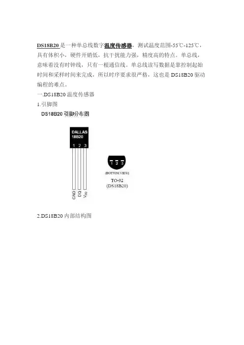
一.DS18B20温度传感器1.引脚图2.DS18B20内部结构图主要由2部分组成:64位ROM、9字节暂存器,如图所示。
(1) 64 位ROM。
它的内容是64 位序列号,它可以被看作是该DS18B20 的地址序列码,其作用是使每个DS18B20 都各不相同,这样就可以实现一根总线上挂接多个DS18B20 的目的。
(2) 9字节暂存器包含:温度传感器、上限触发TH高温报警器、下限触发TL低温报警器、高速暂存器、8位CRC产生器。
3.64位ROM结构图8位CRC:是单总线系列器件的编码,DS18B20定义为28H。
48位序列号:是一个唯一的序列号。
8位系列码:由CRC产生器生产,作为ROM中的前56位编码的校验码。
4.9字节暂存器结构图以上是内部9 个字节的暂存单元(包括EEPROM)。
字节0~1 是温度存储器,用来存储转换好的温度。
字节2~3 是用户用来设置最高报警和最低报警值。
这个可以用软件来实现。
字节4 是配置寄存器,用来配置转换精度,让它工作在9~12 位。
字节5~7 保留位。
字节8 CRC校验位。
是64位ROM中的前56位编码的校验码。
由CRC发生器产生。
5.温度寄存器结构图温度寄存器由两个字节组成,分为低8位和高8位。
一共16位。
其中,第0位到第3位,存储的是温度值的小数部分。
第4位到第10位存储的是温度值的整数部分。
第11位到第15位为符号位。
全0表示是正温度,全1表示是负温度。
表格中的数值,如果相应的位为1,表示存在。
如果相应的位为0,表示不存在。
6.配置寄存器精度值:9-bit 0.5℃10-bit 0.25℃11-bit 0.125℃12-bit 0.0625℃7.温度/数据关系注意:如果温度是一个负温度,要将读到的数据减一再取反二.单总线协议1.单总线通信初始化初始化时序包括:主机发出的复位脉冲和从机发出的应答脉冲。
DS18B20中文资料DS18B20是一种数字温度传感器,采用单总线数据传输协议进行通信。
它能够高精度地测量环境温度,并且具有体积小、价格低廉、使用方便等特点。
本文将介绍DS18B20传感器的原理、特性以及应用场景。
一、传感器原理DS18B20传感器采用基于硅的温度传感技术。
其内部集成了温度传感器、模数转换器等电路,以及一组ROM(只读存储器)和RAM(随机存储器)。
传感器通过感应环境温度引起的半导体温度变化,将温度值转换为数字信号输出。
二、传感器特性1. 高精度:DS18B20传感器具有最高精度为±0.5°C的温度测量能力,适用于对于精度要求较高的应用场景。
2. 大量程:传感器可在-55°C至+125°C的温度范围内进行测量,适用于广泛的温度监测需求。
3. 单总线接口:传感器采用单总线接口进行数据传输,仅需要一根数据线,方便集成和使用。
4. 低功耗:传感器工作时的电源电压范围为3V至5.5V,具有低功耗的特点,适用于需要长时间连续监测温度的场景。
5. 独特的硬件地址:每个DS18B20传感器都有一个独特的64位硬件地址,可以通过该地址进行单独的识别和通信。
三、传感器应用由于DS18B20传感器具有小巧、精确、方便等特点,因此在很多领域得到了广泛应用。
1. 温度监测系统:传感器可以应用于各种温度监测系统,如气象站、冷链物流、温度报警器等。
通过使用多个DS18B20传感器,可以实现对不同位置的温度进行监测和记录。
2. 温度控制系统:传感器可以用于控制温度的系统,例如恒温器、温室控制系统等。
通过实时监测环境温度,并根据需求进行温度控制,可以提供更舒适的生活和工作环境。
3. 工业自动化:在工业环境中,温度监测也是很重要的一项任务。
DS18B20传感器可以与PLC、SCADA等系统集成,用于工业自动化控制和监测。
4. 物联网应用:随着物联网的发展,温度传感器在物联网应用中的需求越来越大。

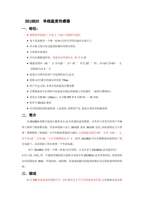
分辨率可编程单总线数字温度传感器——DS18B20 特征:独特单总线接口,只需要一个端口引脚线即可实现通信每个器件的片上ROM 有一个独特64 位串行码存储多点能力使分布式温度检测应用得到简化不需要外围元件能用数据线供电,供电的范围3.0V~5.5V测量温度的范围:-55℃~+125℃(-67℉~+257℉)从-10℃~+85℃的测量的精度是±0.5℃温度传感器分别率由用户从9-12 位中选择在750ms 内把温度转换为12 位数字字(最大值)用户可定义,非易失性温度告警设置告警搜索命令识别和寻址温度在编定的极限之外的器件(温度告警情况)可采用8 引脚SO(150mil)、8 引脚µSOP 和3 引脚TO-92 封装软件兼容DS1822 器件应用范围包括:恒温控制、工业系统、消费类产品、温度计和任何的热敏系统图1 DS18B20 引脚排列图引脚说明:GND—地DQ—数字输入输出VDD—供电电压NC—空连接一般说明:DS18B20 数字温度传感器提供9~12 位摄氏温度的测量,拥有非易失性用户可编程最高与最低触发点告警功能。
DS18B20 通过单总线实现通信,单总线通常是DS18B20 连接。
它能够感应温度的范围为-55℃~+125℃,在-10℃~+85℃的测量的精度是±0.5℃,而且DS18B20 可以直接从数据线上获取供电(寄生电源)而不需要一个额外的外部电源。
因为每个DS18B20 拥有一个独特的64 序列号,因此它允许多个DS18B20 在一条单总线上,所以很方便使用一个微控制器来控制多个分布在较大范围内的DS18B20。
受益于这一特性的应用包括HAVC 环境控制、建筑物、设备和机械内的温度监测、以及过程监测和控制过程的温度监测。
图2注意: A "+"符号在封装上也标有。
订购信息表1S O* µSOP * TO-924 4 15 1 23 8 3DS18B20 详细引脚说明号符明说GND 地当脚引线总单路开,脚引出输入输据数,DQ 生寄见(供件器给时式模源电生寄用使电)分部源电VDD 选可下式模作操源电生寄在脚引,VDDVDD 地接须必* 表中所有未列出的引脚都是NC(空接)概述:方框图3 给出了表一所描述的DS18B20 的主要引脚连接。
DS18B20 单线温度传感器一.特征:●独特的单线接口,只需 1 个接口引脚即可通信●每个设备都有一个唯一的64位串行代码存储在光盘片上●多点能力使分布式温度检测应用得以简化●不需要外部部件●可以从数据线供电,电源电压范围为3。
0V至5.5V●测量范围从—55 ° C至+125 ° C(—67 ° F至257 ° F),从-10℃至+85 ° C的精度为0.5 °C●温度计分辨率是用户可选择的9至12位●转换12位数字的最长时间是750ms●用户可定义的非易失性的温度告警设置●告警搜索命令识别和寻址温度在编定的极限之外的器件(温度告警情况)●采用8引脚SO(150mil),8引脚SOP和3引脚TO — 92封装●软件与DS1822兼容●应用范围包括恒温控制工业系统消费类产品温度计或任何热敏系统二.简介该DS18B20的数字温度计提供9至12位的摄氏温度测量,并具有与非易失性用户可编程上限和下限报警功能。
信息单线接口送入 DS1820 或从 DS1820 送出,因此按照定义只需要一条数据线(和地线)与中央微处理器进行通信.它的测温范围从-55 °C到 +125 ° C,其中从-10 °C至+85 °C可以精确到0。
5°C 。
此外,DS18B20可以从数据线直接供电(“寄生电源”),从而消除了供应需要一个外部电源。
每个 DS18B20 的有一个唯一的64位序列码,它允许多个DS18B20s的功能在同一1-巴士线。
因此,用一个微处理器控制大面积分布的许多DS18B20s是非常简单的。
此特性的应用范围包括 HVAC、环境控制、建筑物、设备或机械内的温度检测以及过程监视和控制系统。
三.综述64位ROM存储设备的独特序号。
存贮器包含2个字节的温度寄存器,它存储来自温度传感器的数字输出.此外,暂存器可以访问的1个字节的上下限温度告警触发器(TH和TL)和1个字节的配置寄存器。

单总线温度传感器DS18B20简介DS18B20是DALLAS公司生产的单总线式数字温度传感器,它具有微型化、低功耗、高性能、搞干扰能力强、易配处理器等优点,特别适用于构成多点温度测控系统,可直接将温度转化成串行数字信号(提供9位二进制数字)给单片机处理,且在同一总线上可以挂接多个传感器芯片。
它具有3引脚TO-92小体积封装形式,温度测量范围为-55℃~+125℃,可编程为9位~12位A/D转换精度,测温分辨率可达0.0625℃,被测温度用符号扩展的16位数字量方式串行输出,其工作电源既可在远端引入,也可采用寄生电源方式产生,多个DS18B20可以并联到3根或2根线上,CPU只需一根端口线就能与多个DS18B20通信,占用微处理器的端口较少,可节省大量的引线和逻辑电路。
以上特点使DS18B20非常适用于远距离多点温度检测系统。
DS18B20外形及引脚说明外形及引脚如图2所示:图2 管脚排列图在TO-92和SO-8的封装中引脚有所不同,具体差别请查阅PDF手册,在TO-92封装中引脚分配如下:1(GND):地2(DQ):单线运用的数据输入输出引脚3(VDD):可选的电源引脚DS18B20工作过程及时序DS18B20内部的低温度系数振荡器是一个振荡频率随温度变化很小的振荡器,为计数器1提供一频率稳定的计数脉冲。
高温度系数振荡器是一个振荡频率对温度很敏感的振荡器,为计数器2提供一个频率随温度变化的计数脉冲。
初始时,温度寄存器被预置成-55℃,每当计数器1从预置数开始减计数到0时,温度寄存器中寄存的温度值就增加1℃,这个过程重复进行,直到计数器2计数到0时便停止。
初始时,计数器1预置的是与-55℃相对应的一个预置值。
以后计数器1每一个循环的预置数都由斜率累加器提供。
为了补偿振荡器温度特性的非线性性,斜率累加器提供的预置数也随温度相应变化。
计数器1的预置数也就是在给定温度处使温度寄存器寄存值增加1℃计数器所需要的计数个数。

DS18B20温度传感器使⽤简介DS18xx系列温度传感器是数字式温度传感器,相对于传统温度传感器精度⾼、稳定性好、电路简单、控制⽅便,在这⾥以DS18B20为例做简单应⽤介绍。
详细资料请参阅芯⽚⼿册。
⼀、特性:(1)应⽤中不需要外部任何元器件即可实现测温电路。
(2)测温范围-55~+125℃,最⼤精度0.0625℃。
(3)只通过⼀条数据线即可实现通信。
(4)每个DS1820器件上都有独⼀⽆⼆的序列号,所以⼀条数据线上可以挂接很多该传感器。
(5)内部有温度上、下限告警功能。
⼆、操作简介DS18B20⼯作时需要接收特定的指令来完成相应功能(指令,可以简单的理解为可以被识别并有相应意义的⼀系列⾼低电平信号),它的指令可分为ROM指令和RAM指令;ROM指令主要对其内部的ROM进⾏操作,如查所使⽤DS18B20的序列号等,如果只使⽤⼀个DS18B20,ROM操作⼀般就可以直接跳过了;RAM指令主要是完成对其内RAM中的数据进⾏操作,如让其开始进⾏数据采集、读数据等。
DS18B20数字温度传感器是单总线器件,数据的读写只通过⼀条数据线进⾏并且这⼀条线上允许挂很多该传感器;这样对器件进⾏读写指令时就会⿇烦⼀些,必须应⽤特定时序来识别⾼低电平信号(如写⾼电平1,并不是把数据线直接拉⾼,⽽是⽤有⼀定时序关系的⾼低电平来代表写1),所以指令表中的0、1在写给DS18B20时就得变成代表0、1电平的时序段序列。
同样,从DS18B20读数据时,也是由特定的时序来完成数据读取。
对DS18B20进⾏读写的时序图如下:硬件连接⽅式有两种,⼀种是由单独电源供电(3~5V);第⼆种是由数据线为DS18B20供电(⼯作速度相对较慢)。
单独电源供电⽅式数据线为DS1820供电⽅式三、DS1820的⼯作过程:1. 复位操作2. 执⾏ROM操作的5条指令之⼀:1)读ROM,2)匹配ROM,3)搜索ROM,4)跳过ROM,5)报警搜索。
DS18B20数字温度传感器接线方便,封装成后可应用于多种场合,如管道式,螺纹式,磁铁吸附式,不锈钢封装式,型号多种多样,有LTM8877,LTM8874等等。
主要根据应用场合的不同而改变其外观。
封装后的DS18B20可用于电缆沟测温,高炉水循环测温,锅炉测温,机房测温,农业大棚测温,洁净室测温,弹药库测温等各种非极限温度场合。
耐磨耐碰,体积小,使用方便,封装形式多样,适用于各种狭小空间设备数字测温和控制领域。
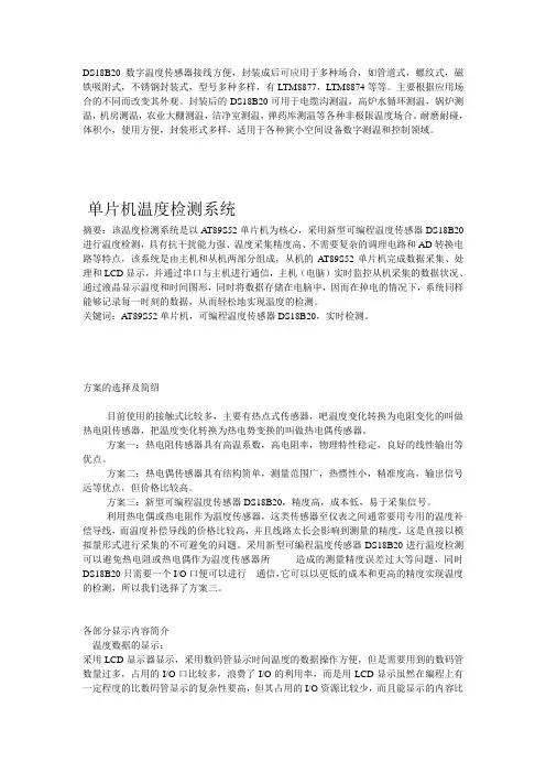
单片机温度检测系统摘要:该温度检测系统是以AT89S52单片机为核心,采用新型可编程温度传感器DS18B20进行温度检测,具有抗干扰能力强、温度采集精度高、不需要复杂的调理电路和AD转换电路等特点,该系统是由主机和从机两部分组成,从机的AT89S52单片机完成数据采集、处理和LCD显示,并通过串口与主机进行通信,主机(电脑)实时监控从机采集的数据状况、通过液晶显示温度和时间图形,同时将数据存储在电脑中,因而在掉电的情况下,系统同样能够记录每一时刻的数据,从而轻松地实现温度的检测。
关键词:AT89S52单片机,可编程温度传感器DS18B20,实时检测。
方案的选择及简绍目前使用的接触式比较多,主要有热点式传感器,吧温度变化转换为电阻变化的叫做热电阻传感器,把温度变化转换为热电势变换的叫做热电偶传感器。
方案一:热电阻传感器具有高温系数,高电阻率,物理特性稳定,良好的线性输出等优点。
方案二:热电偶传感器具有结构简单,测量范围广,热惯性小,精准度高,输出信号远等优点,但价格比较高。
方案三:新型可编程温度传感器DS18B20,精度高,成本低,易于采集信号。
利用热电偶或热电阻作为温度传感器,这类传感器至仪表之间通常要用专用的温度补偿导线,而温度补偿导线的价格比较高,并且线路太长会影响到测量的精度,这是直接以模拟量形式进行采集的不可避免的问题。
采用新型可编程温度传感器DS18B20进行温度检测可以避免热电阻或热电偶作为温度传感器所造成的测量精度误差过大等问题,同时DS18B20只需要一个I/O口便可以进行通信,它可以以更低的成本和更高的精度实现温度的检测,所以我们选择了方案三。
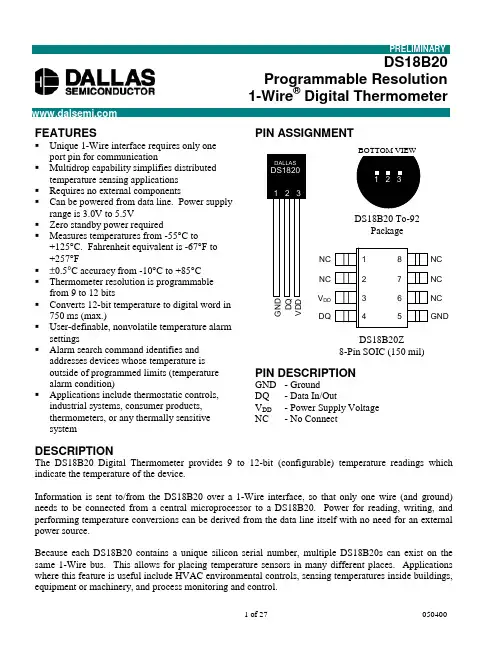
FEATURES Unique 1-Wire interface requires only one port pin for communicationMultidrop capability simplifies distributed temperature sensing applications Requires no external componentsCan be powered from data line. Power supply range is 3.0V to 5.5VZero standby power requiredMeasures temperatures from -55°C to +125°C. Fahrenheit equivalent is -67°F to +257°F±0.5°C accuracy from -10°C to +85°C Thermometer resolution is programmable from 9 to 12 bitsConverts 12-bit temperature to digital word in 750 ms (max.)User-definable, nonvolatile temperature alarm settingsAlarm search command identifies and addresses devices whose temperature is outside of programmed limits (temperature alarm condition)Applications include thermostatic controls,industrial systems, consumer products,thermometers, or any thermally sensitive systemPIN ASSIGNMENTPIN DESCRIPTIONGND - Ground DQ - Data In/OutV DD - Power Supply Voltage NC- No ConnectDESCRIPTIONThe DS18B20 Digital Thermometer provides 9 to 12-bit (configurable) temperature readings which indicate the temperature of the device.Information is sent to/from the DS18B20 over a 1-Wire interface, so that only one wire (and ground)needs to be connected from a central microprocessor to a DS18B20. Power for reading, writing, and performing temperature conversions can be derived from the data line itself with no need for an external power source.Because each DS18B20 contains a unique silicon serial number, multiple DS18B20s can exist on the same 1-Wire bus. This allows for placing temperature sensors in many different places. Applications where this feature is useful include HVAC environmental controls, sensing temperatures inside buildings,equipment or machinery, and process monitoring and control.DS18B20Programmable Resolution 1-Wire ®Digital ThermometerG N D D Q V DDDS18B20 To-92PackageNC NC NC GNDNC NCV DD DQDS18B20Z8-Pin SOIC (150 mil)DETAILED PIN DESCRIPTION Table 1PIN8PIN SOICPINTO92SYMBOL DESCRIPTION51GND Ground.42DQ Data Input/Output pin. For 1-Wire operation: Opendrain. (See “Parasite Power” section.)33V DD Optional V DD pin. See “Parasite Power” section fordetails of connection. V DD must be grounded foroperation in parasite power mode.DS18B20Z (8-pin SOIC): All pins not specified in this table are not to be connected.OVERVIEWThe block diagram of Figure 1 shows the major components of the DS18B20. The DS18B20 has four main data components: 1) 64-bit lasered ROM, 2) temperature sensor, 3) nonvolatile temperature alarm triggers TH and TL, and 4) a configuration register. The device derives its power from the 1-Wire communication line by storing energy on an internal capacitor during periods of time when the signal line is high and continues to operate off this power source during the low times of the 1-Wire line until it returns high to replenish the parasite (capacitor) supply. As an alternative, the DS18B20 may also be powered from an external 3 volt - 5.5 volt supply.Communication to the DS18B20 is via a 1-Wire port. With the 1-Wire port, the memory and control functions will not be available before the ROM function protocol has been established. The master must first provide one of five ROM function commands: 1) Read ROM, 2) Match ROM, 3) Search ROM, 4) Skip ROM, or 5) Alarm Search. These commands operate on the 64-bit lasered ROM portion of each device and can single out a specific device if many are present on the 1-Wire line as well as indicate to the bus master how many and what types of devices are present. After a ROM function sequence has been successfully executed, the memory and control functions are accessible and the master may then provide any one of the six memory and control function commands.One control function command instructs the DS18B20 to perform a temperature measurement. The result of this measurement will be placed in the DS18B20’s scratch-pad memory, and may be read by issuing a memory function command which reads the contents of the scratchpad memory. The temperature alarm triggers TH and TL consist of 1 byte EEPROM each. If the alarm search command is not applied to the DS18B20, these registers may be used as general purpose user memory. The scratchpad also contains a configuration byte to set the desired resolution of the temperature to digital conversion. Writing TH, TL, and the configuration byte is done using a memory function command. Read access to these registers is through the scratchpad. All data is read and written least significant bit first.DS18B20 BLOCK DIAGRAM Figure 1PARASITE POWERThe block diagram (Figure 1) shows the parasite-powered circuitry. This circuitry “steals” power whenever the DQ or V DD pins are high. DQ will provide sufficient power as long as the specified timing and voltage requirements are met (see the section titled “1-Wire Bus System”). The advantages of parasite power are twofold: 1) by parasiting off this pin, no local power source is needed for remote sensing of temperature, and 2) the ROM may be read in absence of normal power.In order for the DS18B20 to be able to perform accurate temperature conversions, sufficient power must be provided over the DQ line when a temperature conversion is taking place. Since the operating current of the DS18B20 is up to 1.5 mA, the DQ line will not have sufficient drive due to the 5k pullup resistor.This problem is particularly acute if several DS18B20s are on the same DQ and attempting to convert simultaneously.There are two ways to assure that the DS18B20 has sufficient supply current during its active conversion cycle. The first is to provide a strong pullup on the DQ line whenever temperature conversions or copies to the E 2 memory are taking place. This may be accomplished by using a MOSFET to pull the DQ line directly to the power supply as shown in Figure 2. The DQ line must be switched over to the strong pull-up within 10 µs maximum after issuing any protocol that involves copying to the E 2 memory or initiates temperature conversions. When using the parasite power mode, the V DD pin must be tied to ground.Another method of supplying current to the DS18B20 is through the use of an external power supply tied to the V DD pin, as shown in Figure 3. The advantage to this is that the strong pullup is not required on the DQ line, and the bus master need not be tied up holding that line high during temperature conversions.This allows other data traffic on the 1-Wire bus during the conversion time. In addition, any number of DS18B20s may be placed on the 1-Wire bus, and if they all use external power, they may all simultaneously perform temperature conversions by issuing the Skip ROM command and then issuing the Convert T command. Note that as long as the external power supply is active, the GND pin may not be floating.The use of parasite power is not recommended above 100°C, since it may not be able to sustain communications given the higher leakage currents the DS18B20 exhibits at these temperatures. For applications in which such temperatures are likely, it is strongly recommended that V DD be applied to the DS18B20.DQVFor situations where the bus master does not know whether the DS18B20s on the bus are parasite powered or supplied with external V DD, a provision is made in the DS18B20 to signal the power supply scheme used. The bus master can determine if any DS18B20s are on the bus which require the strong pullup by sending a Skip ROM protocol, then issuing the read power supply command. After this command is issued, the master then issues read time slots. The DS18B20 will send back “0” on the 1-Wire bus if it is parasite powered; it will send back a “1” if it is powered from the V DD pin. If the master receives a “0,” it knows that it must supply the strong pullup on the DQ line during temperature conversions. See “Memory Command Functions” section for more detail on this command protocol. STRONG PULLUP FOR SUPPLYING DS18B20 DURING TEMPERATURE CONVERSION Figure 2USING V DD TO SUPPLY TEMPERATURE CONVERSION CURRENT Figure 3TO OTHER 1-WIRE DEVICESOPERATION - MEASURING TEMPERATUREThe core functionality of the DS18B20 is its direct-to-digital temperature sensor. The resolution of the DS18B20 is configurable (9, 10, 11, or 12 bits), with 12-bit readings the factory default state. This equates to a temperature resolution of 0.5°C, 0.25°C, 0.125°C, or 0.0625°C. Following the issuance of the Convert T [44h] command, a temperature conversion is performed and the thermal data is stored in the scratchpad memory in a 16-bit, sign-extended two’s complement format. The temperature information can be retrieved over the 1-Wire interface by issuing a Read Scratchpad [BEh] command once the conversion has been performed. The data is transferred over the 1-Wire bus, LSB first. The MSB of the temperature register contains the “sign” (S) bit, denoting whether the temperature is positive or negative.Table 2 describes the exact relationship of output data to measured temperature. The table assumes 12-bit resolution. If the DS18B20 is configured for a lower resolution, insignificant bits will contain zeros. For Fahrenheit usage, a lookup table or conversion routine must be used.Temperature/Data Relationships Table 2232221202-12-22-32-4LSBMSb(unit = °C)LSbS S S S S262524MSBTEMPERATURE DIGITAL OUTPUT(Binary)DIGITAL OUTPUT (Hex)+125°C0000 0111 1101 000007D0h+85°C0000 0101 0101 00000550h*+25.0625°C0000 0001 1001 00010191h+10.125°C0000 0000 1010 001000A2h+0.5°C0000 0000 0000 10000008h0°C0000 0000 0000 00000000h-0.5°C1111 1111 1111 1000FFF8h-10.125°C1111 1111 0101 1110FF5Eh-25.0625°C1111 1110 0110 1111FF6Fh-55°C1111 1100 1001 0000FC90h*The power on reset register value is +85°C.OPERATION - ALARM SIGNALINGAfter the DS18B20 has performed a temperature conversion, the temperature value is compared to the trigger values stored in TH and TL. Since these registers are 8-bit only, bits 9-12 are ignored for comparison. The most significant bit of TH or TL directly corresponds to the sign bit of the 16-bit temperature register. If the result of a temperature measurement is higher than TH or lower than TL, an alarm flag inside the device is set. This flag is updated with every temperature measurement. As long as the alarm flag is set, the DS18B20 will respond to the alarm search command. This allows many DS18B20s to be connected in parallel doing simultaneous temperature measurements. If somewhere the temperature exceeds the limits, the alarming device(s) can be identified and read immediately without having to read non-alarming devices.64-BIT LASERED ROMEach DS18B20 contains a unique ROM code that is 64-bits long. The first 8 bits are a 1-Wire family code (DS18B20 code is 28h). The next 48 bits are a unique serial number. The last 8 bits are a CRC of the first 56 bits. (See Figure 4.) The 64-bit ROM and ROM Function Control section allow the DS18B20 to operate as a 1-Wire device and follow the 1-Wire protocol detailed in the section “1-Wire Bus System.” The functions required to control sections of the DS18B20 are not accessible until the ROM function protocol has been satisfied. This protocol is described in the ROM function protocol flowchart (Figure 5). The 1-Wire bus master must first provide one of five ROM function commands: 1) Read ROM, 2) Match ROM, 3) Search ROM, 4) Skip ROM, or 5) Alarm Search. After a ROM function sequence has been successfully executed, the functions specific to the DS18B20 are accessible and the bus master may then provide one of the six memory and control function commands.CRC GENERATIONThe DS18B20 has an 8-bit CRC stored in the most significant byte of the 64-bit ROM. The bus master can compute a CRC value from the first 56-bits of the 64-bit ROM and compare it to the value stored within the DS18B20 to determine if the ROM data has been received error-free by the bus master. The equivalent polynomial function of this CRC is:CRC = X8 + X5 + X4 + 1The DS18B20 also generates an 8-bit CRC value using the same polynomial function shown above and provides this value to the bus master to validate the transfer of data bytes. In each case where a CRC is used for data transfer validation, the bus master must calculate a CRC value using the polynomial function given above and compare the calculated value to either the 8-bit CRC value stored in the 64-bit ROM portion of the DS18B20 (for ROM reads) or the 8-bit CRC value computed within the DS18B20 (which is read as a ninth byte when the scratchpad is read). The comparison of CRC values and decision to continue with an operation are determined entirely by the bus master. There is no circuitry inside the DS18B20 that prevents a command sequence from proceeding if the CRC stored in or calculated by the DS18B20 does not match the value generated by the bus master.The 1-Wire CRC can be generated using a polynomial generator consisting of a shift register and XOR gates as shown in Figure 6. Additional information about the Dallas 1-Wire Cyclic Redundancy Check is available in Application Note 27 entitled “Understanding and Using Cyclic Redundancy Checks with Dallas Semiconductor Touch Memory Products.”The shift register bits are initialized to 0. Then starting with the least significant bit of the family code, 1 bit at a time is shifted in. After the 8th bit of the family code has been entered, then the serial number is entered. After the 48th bit of the serial number has been entered, the shift register contains the CRC value. Shifting in the 8 bits of CRC should return the shift register to all 0s.64-BIT LASERED ROM Figure 48-BIT CRC CODE48-BIT SERIAL NUMBER 8-BIT FAMILY CODE(28h)MSB LSB MSB LSB MSB LSBROM FUNCTIONS FLOW CHART Figure 51-WIRE CRC CODE Figure 6MEMORYThe DS18B20’s memory is organized as shown in Figure 8. The memory consists of a scratchpad RAM and a nonvolatile, electrically erasable (E 2) RAM, which stores the high and low temperature triggers TH and TL, and the configuration register. The scratchpad helps insure data integrity when communicating over the 1-Wire bus. Data is first written to the scratchpad using the Write Scratchpad [4Eh] command.It can then be verified by using the Read Scratchpad [BEh] command. After the data has been verified, a Copy Scratchpad [48h] command will transfer the data to the nonvolatile (E 2) RAM. This process insures data integrity when modifying memory. The DS18B20 EEPROM is rated for a minimum of 50,000writes and 10 years data retention at T = +55°C.The scratchpad is organized as eight bytes of memory. The first 2 bytes contain the LSB and the MSB of the measured temperature information, respectively. The third and fourth bytes are volatile copies of TH and TL and are refreshed with every power-on reset. The fifth byte is a volatile copy of the configuration register and is refreshed with every power-on reset. The configuration register will be explained in more detail later in this section of the datasheet. The sixth, seventh, and eighth bytes are used for internal computations, and thus will not read out any predictable pattern.It is imperative that one writes TH, TL, and config in succession; i.e. a write is not valid if one writes only to TH and TL, for example, and then issues a reset. If any of these bytes must be written, all three must be written before a reset is issued.There is a ninth byte which may be read with a Read Scratchpad [BEh] command. This byte contains a cyclic redundancy check (CRC) byte which is the CRC over all of the eight previous bytes. This CRC is implemented in the fashion described in the section titled “CRC Generation”.Configuration RegisterThe fifth byte of the scratchpad memory is the configuration register.It contains information which will be used by the device to determine the resolution of the temperature to digital conversion. The bits are organized as shown in Figure 7.DS18B20 CONFIGURATION REGISTER Figure 70R1R011111MSbLSbBits 0-4 are don’t cares on a write but will always read out “1”.Bit 7 is a don’t care on a write but will always read out “0”.R0, R1: Thermometer resolution bits. Table 3 below defines the resolution of the digital thermometer,based on the settings of these 2 bits. There is a direct tradeoff between resolution and conversion time, as depicted in the AC Electrical Characteristics. The factory default of these EEPROM bits is R0=1 and R1=1 (12-bit conversions).Thermometer Resolution Configuration Table 3R1R0Thermometer Resolution Max ConversionTime009 bit 93.75 ms (t conv/8)0110 bit 187.5 ms (t conv /4)1011 bit 375 ms (t conv /2)1112 bit750 ms (t conv )DS18B20 MEMORY MAP Figure 8SCRATCHPADBYTE012345678E 2RAM1-WIRE BUS SYSTEMThe 1-Wire bus is a system which has a single bus master and one or more slaves. The DS18B20 behaves as a slave. The discussion of this bus system is broken down into three topics: hardware configuration, transaction sequence, and 1-Wire signaling (signal types and timing).HARDWARE CONFIGURATIONThe 1-Wire bus has only a single line by definition; it is important that each device on the bus be able to drive it at the appropriate time. To facilitate this, each device attached to the 1-Wire bus must have open drain or 3-state outputs. The 1-Wire port of the DS18B20 (DQ pin) is open drain with an internal circuit equivalent to that shown in Figure 9. A multidrop bus consists of a 1-Wire bus with multiple slaves attached. The 1-Wire bus requires a pullup resistor of approximately 5 kΩ.HARDWARE CONFIGURATION Figure 9The idle state for the 1-Wire bus is high. If for any reason a transaction needs to be suspended, the bus MUST be left in the idle state if the transaction is to resume. Infinite recovery time can occur between bits so long as the 1-Wire bus is in the inactive (high) state during the recovery period. If this does not occur and the bus is left low for more than 480 µs, all components on the bus will be reset. TRANSACTION SEQUENCEThe protocol for accessing the DS18B20 via the 1-Wire port is as follows:InitializationROM Function CommandMemory Function CommandTransaction/DataINITIALIZATIONAll transactions on the 1-Wire bus begin with an initialization sequence. The initialization sequence consists of a reset pulse transmitted by the bus master followed by presence pulse(s) transmitted by the slave(s).The presence pulse lets the bus master know that the DS18B20 is on the bus and is ready to operate. For more details, see the “1-Wire Signaling” section.ROM FUNCTION COMMANDSOnce the bus master has detected a presence, it can issue one of the five ROM function commands. All ROM function commands are 8 bits long. A list of these commands follows (refer to flowchart in Figure 5):Read ROM [33h]This command allows the bus master to read the DS18B20’s 8-bit family code, unique 48-bit serial number, and 8-bit CRC. This command can only be used if there is a single DS18B20 on the bus. If more than one slave is present on the bus, a data collision will occur when all slaves try to transmit at the same time (open drain will produce a wired AND result).Match ROM [55h]The match ROM command, followed by a 64-bit ROM sequence, allows the bus master to address a specific DS18B20 on a multidrop bus. Only the DS18B20 that exactly matches the 64-bit ROM sequence will respond to the following memory function command. All slaves that do not match the 64-bit ROM sequence will wait for a reset pulse. This command can be used with a single or multiple devices on the bus.Skip ROM [CCh]This command can save time in a single drop bus system by allowing the bus master to access the memory functions without providing the 64-bit ROM code. If more than one slave is present on the bus and a Read command is issued following the Skip ROM command, data collision will occur on the bus as multiple slaves transmit simultaneously (open drain pulldowns will produce a wired AND result). Search ROM [F0h]When a system is initially brought up, the bus master might not know the number of devices on the 1-Wire bus or their 64-bit ROM codes. The search ROM command allows the bus master to use a process of elimination to identify the 64-bit ROM codes of all slave devices on the bus.Alarm Search [ECh]The flowchart of this command is identical to the Search ROM command. However, the DS18B20 will respond to this command only if an alarm condition has been encountered at the last temperature measurement. An alarm condition is defined as a temperature higher than TH or lower than TL. The alarm condition remains set as long as the DS18B20 is powered up, or until another temperature measurement reveals a non-alarming value. For alarming, the trigger values stored in EEPROM are taken into account. If an alarm condition exists and the TH or TL settings are changed, another temperature conversion should be done to validate any alarm conditions.Example of a ROM SearchThe ROM search process is the repetition of a simple three-step routine: read a bit, read the complement of the bit, then write the desired value of that bit. The bus master performs this simple, three-step routine on each bit of the ROM. After one complete pass, the bus master knows the contents of the ROM in one device. The remaining number of devices and their ROM codes may be identified by additional passes.The following example of the ROM search process assumes four different devices are connected to the same 1-Wire bus. The ROM data of the four devices is as shown:ROM100110101...ROM210101010...ROM311110101...ROM400010001...The search process is as follows:1.The bus master begins the initialization sequence by issuing a reset pulse. The slave devices respondby issuing simultaneous presence pulses.2.The bus master will then issue the Search ROM command on the 1-Wire bus.3.The bus master reads a bit from the 1-Wire bus. Each device will respond by placing the value of thefirst bit of their respective ROM data onto the 1-Wire bus. ROM1 and ROM4 will place a 0 onto the 1-Wire bus, i.e., pull it low. ROM2 and ROM3 will place a 1 onto the 1-Wire bus by allowing the line to stay high. The result is the logical AND of all devices on the line, therefore the bus master sees a 0. The bus master reads another bit. Since the Search ROM data command is being executed, all of the devices on the 1-Wire bus respond to this second read by placing the complement of the first bit of their respective ROM data onto the 1-Wire bus. ROM1 and ROM4 will place a 1 onto the 1-Wire, allowing the line to stay high. ROM2 and ROM3 will place a 0 onto the 1-Wire, thus it will be pulled low. The bus master again observes a 0 for the complement of the first ROM data bit. The bus master has determined that there are some devices on the 1-Wire bus that have a 0 in the first position and others that have a 1.The data obtained from the two reads of the three-step routine have the following interpretations:00There are still devices attached which have conflicting bits in this position.01All devices still coupled have a 0-bit in this bit position.10All devices still coupled have a 1-bit in this bit position.11There are no devices attached to the 1-Wire bus.4.The bus master writes a 0. This deselects ROM2 and ROM3 for the remainder of this search pass,leaving only ROM1 and ROM4 connected to the 1-Wire bus.5.The bus master performs two more reads and receives a 0-bit followed by a 1-bit. This indicates thatall devices still coupled to the bus have 0s as their second ROM data bit.6.The bus master then writes a 0 to keep both ROM1 and ROM4 coupled.7.The bus master executes two reads and receives two 0-bits. This indicates that both 1-bits and 0-bitsexist as the 3rd bit of the ROM data of the attached devices.8.The bus master writes a 0-bit. This deselects ROM1, leaving ROM4 as the only device stillconnected.9.The bus master reads the remainder of the ROM bits for ROM4 and continues to access the part ifdesired. This completes the first pass and uniquely identifies one part on the 1-Wire bus.10.The bus master starts a new ROM search sequence by repeating steps 1 through 7.11.The bus master writes a 1-bit. This decouples ROM4, leaving only ROM1 still coupled.12.The bus master reads the remainder of the ROM bits for ROM1 and communicates to the underlyinglogic if desired. This completes the second ROM search pass, in which another of the ROMs was found.13.The bus master starts a new ROM search by repeating steps 1 through 3.14.The bus master writes a 1-bit. This deselects ROM1 and ROM4 for the remainder of this search pass,leaving only ROM2 and ROM3 coupled to the system.15.The bus master executes two Read time slots and receives two 0s.16.The bus master writes a 0-bit. This decouples ROM3 leaving only ROM2.17.The bus master reads the remainder of the ROM bits for ROM2 and communicates to the underlyinglogic if desired. This completes the third ROM search pass, in which another of the ROMs was found.18.The bus master starts a new ROM search by repeating steps 13 through 15.19.The bus master writes a 1-bit. This decouples ROM2, leaving only ROM3.20.The bus master reads the remainder of the ROM bits for ROM3 and communicates to the underlyinglogic if desired. This completes the fourth ROM search pass, in which another of the ROMs was found.NOTE:The bus master learns the unique ID number (ROM data pattern) of one 1-Wire device on each ROM Search operation. The time required to derive the part’s unique ROM code is:960 µs + (8 + 3 x 64) 61 µs = 13.16 msThe bus master is therefore capable of identifying 75 different 1-Wire devices per second.I/O SIGNALINGThe DS18B20 requires strict protocols to insure data integrity. The protocol consists of several types of signaling on one line: reset pulse, presence pulse, write 0, write 1, read 0, and read 1. All of these signals, with the exception of the presence pulse, are initiated by the bus master.The initialization sequence required to begin any communication with the DS18B20 is shown in Figure 11. A reset pulse followed by a presence pulse indicates the DS18B20 is ready to send or receive data given the correct ROM command and memory function command.The bus master transmits (TX) a reset pulse (a low signal for a minimum of 480 µs). The bus master then releases the line and goes into a receive mode (RX). The 1-Wire bus is pulled to a high state via the 5k pullup resistor. After detecting the rising edge on the DQ pin, the DS18B20 waits 15-60 µs and then transmits the presence pulse (a low signal for 60-240 µs).MEMORY COMMAND FUNCTIONSThe following command protocols are summarized in Table 4, and by the flowchart of Figure 10.Write Scratchpad [4Eh]This command writes to the scratchpad of the DS18B20, starting at the TH register. The next 3 bytes written will be saved in scratchpad memory at address locations 2 through 4. All 3 bytes must be written before a reset is issued.Read Scratchpad [BEh]This command reads the contents of the scratchpad. Reading will commence at byte 0 and will continue through the scratchpad until the ninth (byte 8, CRC) byte is read. If not all locations are to be read, the master may issue a reset to terminate reading at any time.Copy Scratchpad [48h]This command copies the scratchpad into the E2memory of the DS18B20, storing the temperature trigger bytes in nonvolatile memory. If the bus master issues read time slots following this command, the DS18B20 will output 0 on the bus as long as it is busy copying the scratchpad to E2; it will return a 1 when the copy process is complete. If parasite-powered, the bus master has to enable a strong pullup for at least 10 ms immediately after issuing this command. The DS18B20 EEPROM is rated for a minimum of 50,000 writes and 10 years data retention at T=+55°C.Convert T [44h]This command begins a temperature conversion. No further data is required. The temperature conversion will be performed and then the DS18B20 will remain idle. If the bus master issues read time slots following this command, the DS18B20 will output 0 on the bus as long as it is busy making a temperature conversion; it will return a 1 when the temperature conversion is complete. If parasite-powered, the bus master has to enable a strong pullup for a period greater than t conv immediately after issuing this command.Recall E2 [B8h]This command recalls the temperature trigger values and configuration register stored in E2 to the scratchpad. This recall operation happens automatically upon power-up to the DS18B20 as well, so valid data is available in the scratchpad as soon as the device has power applied. With every read data time slot issued after this command has been sent, the device will output its temperature converter busy flag: 0=busy, 1=ready.Read Power Supply [B4h]With every read data time slot issued after this command has been sent to the DS18B20, the device will signal its power mode: 0=parasite power, 1=external power supply provided.。
DS18B20中文资料在现代电子技术领域,温度测量是一项非常重要的任务。
而DS18B20 作为一款常用的数字温度传感器,以其出色的性能和简单的接口,在各种温度测量应用中得到了广泛的应用。
DS18B20 是由美国达拉斯半导体公司(Dallas Semiconductor)推出的一款单线数字温度传感器。
它具有体积小、硬件开销低、抗干扰能力强、精度高等优点。
从外观上看,DS18B20 通常采用小型的TO-92 封装或者SOP 封装,这使得它能够轻松集成到各种电路中,占用极小的空间。
在性能方面,DS18B20 的测量范围非常广泛,从-55℃到+125℃,能够满足大多数实际应用场景的温度测量需求。
其测量精度在-10℃到+85℃范围内可达到 ±05℃,这对于很多对温度精度要求较高的场合来说,是非常出色的表现。
DS18B20 之所以能够在众多温度传感器中脱颖而出,很大程度上得益于其独特的单线接口。
这意味着它只需要一根数据线就可以与微控制器进行通信,大大简化了电路设计和布线工作。
在使用 DS18B20 进行温度测量时,首先需要将其正确连接到微控制器。
通常,将 DS18B20 的数据线连接到微控制器的一个通用输入输出引脚(GPIO)上。
然后,通过微控制器发送特定的指令来启动温度转换,并读取转换后的温度值。
DS18B20 的工作原理基于其内部的温度敏感元件和模数转换电路。
当接收到温度转换指令后,传感器内部的温度敏感元件会感知当前环境温度,并将其转换为对应的数字信号,然后通过单线接口传输给微控制器。
在编程方面,不同的微控制器平台可能会有一些差异,但基本的流程大致相同。
一般来说,需要先初始化单线接口,然后发送复位脉冲和搜索 ROM 指令来识别总线上的 DS18B20 设备。
接着,发送启动温度转换指令,并等待转换完成。
最后,读取转换后的温度数据,并进行相应的处理和显示。
为了确保测量的准确性和稳定性,在实际应用中还需要注意一些问题。

D S18B20数字温度传感器介绍目前常用的微机与外设之间进行的数据通信的串行总线主要有 I 2C 总线,SPI 总线等。
其中 I 2C 总线以同步串行 2 线方式进行通信(一条时钟线,一条数据线), SPI 总线则以同步串行 3 线方式进行通信(一条时钟线,一条数据输入线,一条数据输出线)。
这些总线至少需要两条或两条以上的信号线。
而单总线( 1-wire bus ),采用单根信号线,既可传输数据,而且数据传输是双向的, CPU 只需一根端口线就能与诸多单总线器件通信,占用微处理器的端口较少,可节省大量的引线和逻辑电路。
因而,这种单总线技术具有线路简单,硬件开销少,成本低廉,软件设计简单,便于总线扩展和维护。
同时,基于单总线技术能较好地解决传统识别器普遍存在的携带不便,易损坏,易受腐馈,易受电磁干扰等不足,因此,单总线具有广阔的应用前景,是值得关注的一个发展领域。
单总线即只有一根数据线,系统中的数据交换,控制都由这根线完成。
主机或从机通过一个漏极开路或三态端口连至数据线,以允许设备在不发送数据时能够释放总线,而让其它设备使用总线。
单总线通常要求外接一个约为 4.7K 的上拉电阻,这样,当总线闲置时其状态为高电平。
DS18B20 数字式温度传感器,与传统的热敏电阻有所不同的是,使用集成芯片,采用单总线技术,其能够有效的减小外界的干扰,提高测量的精度,同时,它可以直接将被测温度转化成串行数字信号供微机处理,接口简单,使数据传输和处理简单化。
部分功能电路的集成,使总体硬件设计更简洁,能有效地降低成本,搭建电路和焊接电路时更快,调试也更方便简单化,这也就缩短了开发的周期。
DS18B20 单线数字温度传感器,即“一线器件”,其具有独特的优点:( 1 )采用单总线的接口方式与微处理器连接时仅需要一条口线即可实现微处理器与 DS18B20 的双向通讯。
单总线具有经济性好,抗干扰能力强,适合于恶劣环境的现场温度测量,使用方便等优点,使用户可轻松地组建传感器网络,为测量系统的构建引入全新概念。
ds18b20温度传感器工作原理
DS18B20温度传感器是一种数字温度传感器,它基于热电效
应来测量温度。
该传感器由一个精密的温度传感器和一个数字转换器组成。
以下是DS18B20温度传感器的工作原理:
1. 热电效应:DS18B20温度传感器利用热电效应来测量温度。
当两个不同材料的接触点形成温度梯度时,就会产生电动势。
传感器中的温度传感器部分采用的材料对温度变化非常敏感,因此产生的电动势可以反映出温度的变化。
2. 温度传感器:DS18B20温度传感器中的温度传感器部分是
由一个特殊的材料制成的。
该材料具有温度敏感性,当温度变化时,该材料会产生电动势。
这个电动势可以通过传感器的引脚进行读取和转换。
3. 数字转换器:DS18B20温度传感器具有内置的数字转换器。
这个数字转换器可以将从温度传感器获得的电压信号转换为数字信号。
数字信号可以直接读取和处理,而无需进行模拟信号转换。
4. 串行总线通信:DS18B20温度传感器通过一种称为One-
Wire总线的串行通信协议与主控制器进行通信。
传感器和主
控制器之间只需使用单一的数据线进行通信,使得传感器的连接变得简单方便。
总结起来,DS18B20温度传感器工作原理是利用热电效应测
量温度,并通过温度传感器和数字转换器来转换和读取温度信号。
该传感器通过One-Wire总线与主控制器进行通信。
2.2 器件选择2.2.1 温度传感器在现代检测技术中,传感器占据着不可动摇的重要位置。
主机对数据的处理能力已经相当的强,但是对现实世界中的模拟量却无能为力。
如果没有各种精确可靠的传感器对非电量和模拟信号进行检测并提供可靠的数据,那计算机也无法发挥他应有的作用。
传感器把非电量转换为电量,经过放大处理后,转换为数字量输入计算机,由计算机对信号进行分析处理。
从而传感器技术与计算机技术结合起来,对自动化和信息化起重要作用。
采用各种传感器和微处理技术可以对各种工业参数及工业产品进行测控及检验,准确测量产品性能,及时发现隐患。
为提高产品质量、改进产品性能,防止事故发生提供必要的信息和更可靠的数据。
由于系统的工作环境比较恶劣,且对测量要求比较高,所以选择合适的传感器很重要。
目前,国际上新型温度传感器正从模拟式向数字式、从集成化向智能化和网络化的方向飞速发展。
智能温度传感器DS18B20正是朝着高精度、多功能、总线标准化、高可靠性及安全性、开发虚拟传感器和网络传感器、研制单片测温系统等高科技的方向迅速发展。
因此,智能温度传感器DS18B20作为温度测量装置已广泛应用于人民的日常生活和工农业生产中[5]。
2.2.1.1 DS18B20简介DS18B20是美国DALLAS半导体公司继DS1820之后最新推出的一种数字化单总线器件。
属于新一代适配微处理器的改进型智能温度传感器。
与传统的热敏电阻相比,它能够直接读出被测温度,并且可根据实际要求通过简单的编程实现9~12位的数字值读数方式。
可以分别在93.75ms和750ms内完成9位和12位的数字量,并且从DS18B20读出的信息或写入DS18B20的信息仅需要一根口线(单线接口)读写,温度变换功率来源于数据总线,总线本身也可以向所挂接的DS18B20供电,而无需额外电源。
因而使用DS18B20可使系统结构更趋简单,可靠性更高。
同时其“一线总线”独特而且经济的特点,使用户可轻松地组建传感器网络,为测量系统的构建引入了全新的概念。
新型数字温度传感器DS18B20介绍单片机轻松入门教学 ------- 『电子驿站』原创,转载请注明出处!---------------------------------------------------------------------------------------------------------------在传统的模拟信号远距离温度测量系统中,需要很好的解决引线误差补偿问题、多点测量切换误差问题和放大电路零点漂移误差问题等技术问题,才能够达到较高的测量精度。
另外一般监控现场的电磁环境都非常恶劣,各种干扰信号较强,模拟温度信号容易受到干扰而产生测量误差,影响测量精度。
因此,在温度测量系统中,采用抗干扰能力强的新型数字温度传感器是解决这些问题的最有效方案,新型数字温度传感器DS18B20具有体积更小、精度更高、适用电压更宽、采用一线总线、可组网等优点,在实际应用中取得了良好的测温效果。
新的"一线器件"DS18B20体积更小、适用电压更宽、更经济。
美国Dallas半导体公司的数字化温度传感器DS1820是世界上第一片支持 "一线总线"接口的温度传感器,在其内部使用了在板(ON-B0ARD)专利技术。
全部传感元件及转换电路集成在形如一只三极管的集成电路内。
一线总线独特而且经济的特点,使用户可轻松地组建传感器网络,为测量系统的构建引入全新概念。
现在,新一代的DS18B20体积更小、更经济、更灵活。
使你可以充分发挥“一线总线”的优点。
目前DS18B20批量采购价格仅10元左右。
DS18B20、DS1822 "一线总线"数字化温度传感器同DS1820一样,DS18B20也支持"一线总线"接口,测量温度范围为-55°C~+125°C,在-10~+85°C 范围内,精度为±0.5°C。
数字温度传感器DS18B20介绍1、DS18B20的主要特性1.1、适应电压范围更宽,电压范围:3.0~5.5V,在寄生电源方式下可由数据线供电1.2、独特的单线接口方式,DS18B20在与微处理器连接时仅需要一条口线即可实现微处理器与DS18B20的双向通讯1.3、DS18B20支持多点组网功能,多个DS18B20可以并联在唯一的三线上,实现组网多点测温1.4、DS18B20在使用中不需要任何外围元件,全部传感元件及转换电路集成在形如一只三极管的集成电路内1.5、温范围-55℃~+125℃,在-10~+85℃时精度为±0.5℃1.6、可编程的分辨率为9~12位,对应的可分辨温度分别为0.5℃、0.25℃、0.125℃和0.0625℃,可实现高精度测温1.7、在9位分辨率时最多在93.75ms内把温度转换为数字,12位分辨率时最多在750ms内把温度值转换为数字,速度更快1.8、测量结果直接输出数字温度信号,以"一线总线"串行传送给CPU,同时可传送CRC校验码,具有极强的抗干扰纠错能力艾驰商城1.9、负压特性:电源极性接反时,芯片不会因发热而烧毁,但不能正常工作。
2、DS18B20的外形和内部结构DS18B20内部结构主要由四部分组成:64位光刻ROM、温度传感器、非挥发的温度报警触发器TH和TL、配置寄存器。
DS18B20的外形及管脚排列如下图1:DS18B20引脚定义:(1)DQ为数字信号输入/输出端;(2)GND为电源地;(3)VDD为外接供电电源输入端(在寄生电源接线方式时接地)。
图2: DS18B20内部结构图3、DS18B20工作原理DS18B20的读写时序和测温原理与DS1820相同,只是得到的温度值的位数因分辨率不同而不同,且温度转换时的延时时间由2s减为750ms。
DS18B20测温原理如图3所示。
图中低温度系数晶振的振荡频率受温度影响很小,用于产生固定频率的脉冲信号送给计数器1。
温度传感器ds18b20温度传感器DS18B201. 简介温度传感器DS18B20是一种数字温度传感器,可用于测量环境温度。
该传感器由Maxim Integrated公司生产,并在许多应用中得到了广泛的应用,如家庭自动化、气象站、工业控制等。
DS18B20采用了数字化接口,并具有高精度、可编程分辨率和低功耗等特点。
2. 技术规格DS18B20的技术规格如下:- 工作电源:3.0V至5.5V- 测量范围:-55°C至+125°C- 分辨率:可编程为9、10、11或12位- 精度:±0.5°C(在-10°C至+85°C范围内)- 通信接口:一线式数字接口3. 工作原理DS18B20采用了一线式数字接口,这意味着它只需要一根数据线进行通信。
传感器从控制器接收命令,并通过数据线将温度数据发送回控制器。
传感器的数据线同时起到了供电的作用。
DS18B20通过内部的精密温度传感器测量环境温度。
传感器将温度转换为数字信号,并通过数据线将其发送给控制器。
传感器的分辨率可以根据需要进行编程,从而在精度和响应速度之间进行平衡。
4. 使用方法使用DS18B20温度传感器非常简单。
首先,将传感器的电源引脚连接到可用的电源引脚,并将数据线连接到控制器的GPIO引脚。
然后,通过控制器向传感器发送命令,请求温度数据。
传感器将在一段时间后将温度数据发送回控制器,控制器可以读取这些数据并进行相应的处理。
DS18B20还具有一些特殊的命令,如启动温度转换、复位传感器和读取ROM代码等。
这些命令可以通过与控制器的通信来实现。
5. 应用领域温度传感器DS18B20在许多应用中得到了广泛的应用。
以下是一些常见的应用领域:- 家庭自动化:DS18B20可以用于监测室内温度,从而实现智能化的温控系统。
- 气象站:DS18B20可以用于监测室外温度,并将数据发送到气象站系统进行分析和显示。
D S18B20数字温度传感器介绍目前常用的微机与外设之间进行的数据通信的串行总线主要有 I 2C 总线,SPI 总线等。
其中 I 2C 总线以同步串行 2 线方式进行通信(一条时钟线,一条数据线), SPI 总线则以同步串行 3 线方式进行通信(一条时钟线,一条数据输入线,一条数据输出线)。
这些总线至少需要两条或两条以上的信号线。
而单总线( 1-wire bus ),采用单根信号线,既可传输数据,而且数据传输是双向的, CPU 只需一根端口线就能与诸多单总线器件通信,占用微处理器的端口较少,可节省大量的引线和逻辑电路。
因而,这种单总线技术具有线路简单,硬件开销少,成本低廉,软件设计简单,便于总线扩展和维护。
同时,基于单总线技术能较好地解决传统识别器普遍存在的携带不便,易损坏,易受腐馈,易受电磁干扰等不足,因此,单总线具有广阔的应用前景,是值得关注的一个发展领域。
单总线即只有一根数据线,系统中的数据交换,控制都由这根线完成。
主机或从机通过一个漏极开路或三态端口连至数据线,以允许设备在不发送数据时能够释放总线,而让其它设备使用总线。
单总线通常要求外接一个约为 4.7K 的上拉电阻,这样,当总线闲置时其状态为高电平。
DS18B20 数字式温度传感器,与传统的热敏电阻有所不同的是,使用集成芯片,采用单总线技术,其能够有效的减小外界的干扰,提高测量的精度,同时,它可以直接将被测温度转化成串行数字信号供微机处理,接口简单,使数据传输和处理简单化。
部分功能电路的集成,使总体硬件设计更简洁,能有效地降低成本,搭建电路和焊接电路时更快,调试也更方便简单化,这也就缩短了开发的周期。
DS18B20 单线数字温度传感器,即“一线器件”,其具有独特的优点:( 1 )采用单总线的接口方式与微处理器连接时仅需要一条口线即可实现微处理器与 DS18B20 的双向通讯。
单总线具有经济性好,抗干扰能力强,适合于恶劣环境的现场温度测量,使用方便等优点,使用户可轻松地组建传感器网络,为测量系统的构建引入全新概念。
( 2 )测量温度范围宽,测量精度高 DS18B20 的测量范围为 -55 ℃ ~+ 125 ℃ ;在 -10~+ 85°C 范围内,精度为± 0.5°C 。
( 3 )在使用中不需要任何外围元件。
( 4 )持多点组网功能多个 DS18B20 可以并联在惟一的三线上,实现多点测温。
( 5 )供电方式灵活 DS18B20 可以通过内部寄生电路从数据线上获取电源。
因此,当数据线上的时序满足一定的要求时,可以不接外部电源,从而使系统结构更趋简单,可靠性更高。
( 6 )测量参数可配置 DS18B20 的测量分辨率可通过程序设定9~12 位。
( 7 )负压特性电源极性接反时,温度计不会因发热而烧毁,但不能正常工作。
( 8 )掉电保护功能 DS18B20 内部含有 EEPROM ,在系统掉电以后,它仍可保存分辨率及报警温度的设定值。
DS18B20 具有体积更小、适用电压更宽、更经济、可选更小的封装方式,更宽的电压适用范围,适合于构建自己的经济的测温系统,因此也就被设计者们所青睐。
DS18B20的内部结构DS18B20测温原理DS18B20 的内部测温电路框图低温度系数晶振的振荡频率受温度的影响很小,用于产生固定频率的脉冲信号送给减法计数器 1 ,为计数器提供一频率稳定的计数脉冲。
高温度系数晶振随温度变化其震荡频率明显改变,很敏感的振荡器,所产生的信号作为减法计数器 2 的脉冲输入,为计数器 2 提供一个频率随温度变化的计数脉冲。
图中还隐含着计数门,当计数门打开时, DS18B20 就对低温度系数振荡器产生的时钟脉冲后进行计数,进而完成温度测量。
计数门的开启时间由高温度系数振荡器来决定,每次测量前,首先将 -55 ℃ 所对应的基数分别置入减法计数器 1 和温度寄存器中,减法计数器 1 和温度寄存器被预置在 -55 ℃ 所对应的一个基数值。
减法计数器 1 对低温度系数晶振产生的脉冲信号进行减法计数,当减法计数器 1 的预置值减到 0 时温度寄存器的值将加 1 ,减法计数器 1 的预置将重新被装入,减法计数器 1 重新开始对低温度系数晶振产生的脉冲信号进行计数,如此循环直到减法计数器 2 计数到 0 时,停止温度寄存器值的累加,此时温度寄存器中的数值即为所测温度。
斜率累加器用于补偿和修正测温过程中的非线性,其输出用于修正减法计数器的预置值,只要计数门仍未关闭就重复上述过程,直至温度寄存器值达到被测温度值。
DS18B20 的管脚排列及封装图DQ 为数字信号输入 / 输出端; GND 为电源地; VDD 为外接供电电源输入端,电源供电 3.0~5.5V (在寄生电源接线方式时接地)。
寄生电源工作方式外接电源工作方式注意:当温度高于100℃ 时,不能使用寄生电源,因为此时器件中较大的漏电流会使总线不能可靠检测高低电平,从而导致数据传输误码率的增大。
DS18B20 内部结构主要由四部分组成: 64 位光刻 ROM 、温度传感器、非挥发的温度报警触发器 TH 和 TL 、配置寄存器。
光刻 ROM 中的 64 位序列号是出厂前被光刻好的,它可以看作是该DS18B20 的地址序列码。
64 位光刻 ROM 的排列是:开始 8 位(地址:28H )是产品类型标号,接着的 48 位是该 DS18B20 自身的序列号,并且每个DS18B20 的序列号都不相同,因此它可以看作是该 DS18B20 的地址序列码;最后 8 位则是前面 56 位的循环冗余校验码( CRC=X8+X5+X4+1 )。
由于每一个DS18B20 的 ROM 数据都各不相同,因此微控制器就可以通过单总线对多个DS18B20 进行寻址,从而实现一根总线上挂接多个 DS18B20 的目的。
64 b 闪速 ROMDS18B20 中的温度传感器用于完成对温度的测量,它的测量精度可以配置成 9 位, 10 位, 11 位或 12 位 4 种状态。
温度传感器在测量完成后将测量的结果存储在 DS18B20 的两个 8BIT 的 RAM 中,单片机可通过单线接口读到该数据,读取时低位在前,高位在后数据的存储格式如下表(以 12 位转化为例):温度信号寄存器格式这是 12 位转化后得到的 12 位数据,存储在 18B20 的两个 8 比特的 RAM 中,二进制中的前面 5 位是符号位,如果测得的温度大于 0 ,这 5 位为 0 ,只要将测到的数值乘于 0.0625 即可得到实际温度;如果温度小于0 ,这 5 位为 1 ,测到的数值需要取反加 1 再乘于 0.0625 即可得到实际温度。
例如:+ 125 ℃ 的数字输出为07D0H ,+ 25.0625 ℃ 的数字输出为0191H , -25.0625 ℃ 的数字输出为 FF6FH , -55 ℃ 的数字输出为FC90H 。
DS18B20 完成温度转换后,就把测得的温度值与 TH , TL 作比较,若 T>TH 或 T<TL, 则将该器件内的告警标志置位,并对主机发出的告警搜索命令作出响应。
因此,可用多只 DS18B20 同时测量温度并进行告警搜索。
DS18B20 温度传感器的存储器DS18B20 温度传感器的内部存储器包括一个高速暂存 RAM 和一个非易失性的可电擦除的 E2RAM, 后者存放高温度和低温度触发器 TH 、 TL 和结构寄存器。
数据先写入 RAM ,经校验后再传给 E2RAM 。
暂存存储器包含了 8 个连续字节,前两个字节是测得的温度信息,第一个字节的内容是温度的低八位 TL ,第二个字节是温度的高八位 TH 。
第三个和第四个字节是 TH 、 TL 的易失性拷贝,第五个字节是结构寄存器的易失性拷贝,这三个字节的内容在每一次上电复位时被刷新。
第六、七、八个字节用于内部计算。
第九个字节是冗余检验字节,可用来保证通信正确。
DS18B20 的分布如下:DS18B20 的暂存寄存器分布在 64 b ROM 的最高有效字节中存储有循环冗余校验码( CRC )。
主机根据 ROM 的前 56 位来计算 CRC 值,并和存入 DS18B20 中的 CRC 值做比较,以判断主机收到的 ROM 数据是否正确。
设置寄存器设置寄存器位于高速闪存的低5个字节,这个寄存器中的内容被用来确定温度的转换精度。
寄存器各位的内容如下:DS18B20 的设置寄存器各位内容该寄存器的低五位一直都是 1 , TM 是测试模式位,用于设置 DS18B20 在工作模式还是在测试模式。
在 DS18B20 出厂时该位被设置为 0 ,用户不要去改动。
R1 和 R0 用来设置分辨率,如下表所示:( DS18B20 出厂时被设置为 12 位)R1 R0 分辨率温度最大转换时间0 0 9 位93.75 ms0 1 10 位187.5 ms1 0 11 位375 ms0 0 12 位750 ms分辨率设置由表可知,设定的分辨率越高,所需要的温度数据转换时间就越长。
因此,在实际应用中要在分辨率和转换时间权衡考虑。
DS18B20 的温度测量1-WIRE 网络具有严谨的控制结构,其结构如下图所示,一般通过双绞线与 1-WIRE 元件进行数据通信,它们通常被定义为漏极开路端点,主 / 从式多点结构,而且一般都在主机端接上一个上拉电阻 +5V 电源。
通常为了给1-WIRE 设备提供足够的电源,需要一个 MOSFET 管将 1-WIRE 总线上拉至 +5V 电源。
DS18B20 组成的 1-WIRE 网络1-WIRE 网络通信协议是分时定义的,有严格的时隙概念,下图是复位脉冲的时隙。
1-WIRE 协议的复位脉冲时隙1-WIRE 读写“ 0/ 1 ” 时隙DS18B20 单线通信功能是分时完成的,他有严格的时隙概念,如果出现序列混乱, 1-WIRE 器件将不响应主机,因此读写时序很重要。
系统对DS18B20 的各种操作必须按协议进行。
根据 DS18B20 的协议规定,微控制器控制 DS18B20 完成温度的转换必须经过以下 4 个步骤:(1)每次读写前对 DS18B20 进行复位初始化。
复位要求主 CPU 将数据线下拉 500ms ,然后释放, DS18B20 收到信号后等待 16ms~60ms 左右,然后发出 60ms~240ms 的存在低脉冲,主 CPU 收到此信号后表示复位成功。
(2)发送一条 ROM 指令,如下表所示:指令名称指令代码指令功能读 ROM 33H 读 DS18B20ROM 中的编码(即读 64 位地址)ROM 匹配(符合ROM )55H发出此命令之后,接着发出 64 位ROM 编码,访问单总线上与编码相对应 DS18B20 使之作出响应,为下一步对该 DS18B20 的读写作准备搜索 ROM 0F0H 用于确定挂接在同一总线上 DS18B20 的个数和识别 64 位 ROM 地址,为操作各器件作好准备跳过 ROM 0CCH 忽略 64 位 ROM 地址,直接向DS18B20 发温度变换命令,适用于单片机工作警报搜索0ECH 该指令执行后,只有温度超过设定值上限或下限的片子才做出响应DS18B20 的 ROM 指令集(3)发送存储器指令,如下表所示:DS18B20 的存储器指令集(4)进行数据通信。